cover or side panel removed. ● Do not stack computers on top of each other or place computers so near each other that they are subject to each other’s re-circulated or preheated air. ● If the computer is to be operated
mag, kann auch einen Komparator nehmen um die Spannung am Widerstand zu erfassen, oder einen High Side Current Sensor, irgendeine INA halt. Oder die Elektronik untersuchen, reichlich sicher ist da ein Transistor drin der einen Lastwiderstand schaltet. Den kann man rausknipsen und stattdessen ein Relais
nur die Spannung für den Optokoppler runter, dessen LED gegen GND geht. Der Fototransistor ist low-side eingesetzt und der Collector ist mit 10k Pull-Up am ESP angeschlossen. Um den Ruhestrom des Tasters von 0.5mA, der die LED im Optokoppler leicht zum glimmen bringt, "herauszufiltern", ist die Basis
funktioniert leider nicht weil der Mittelpunkt der FET-Halbbrücke (und damit alle Anschlüsse des HighSide-Drivers) trotzdem auf die Eingangsspannung angehoben wird. Mehr als 60V -> LT1339 Cabrio. Andere Controller bzw. DSPs wären zur PWM-Erzeugung natürlich gut geeignet - aber da muss ich leider zugeben
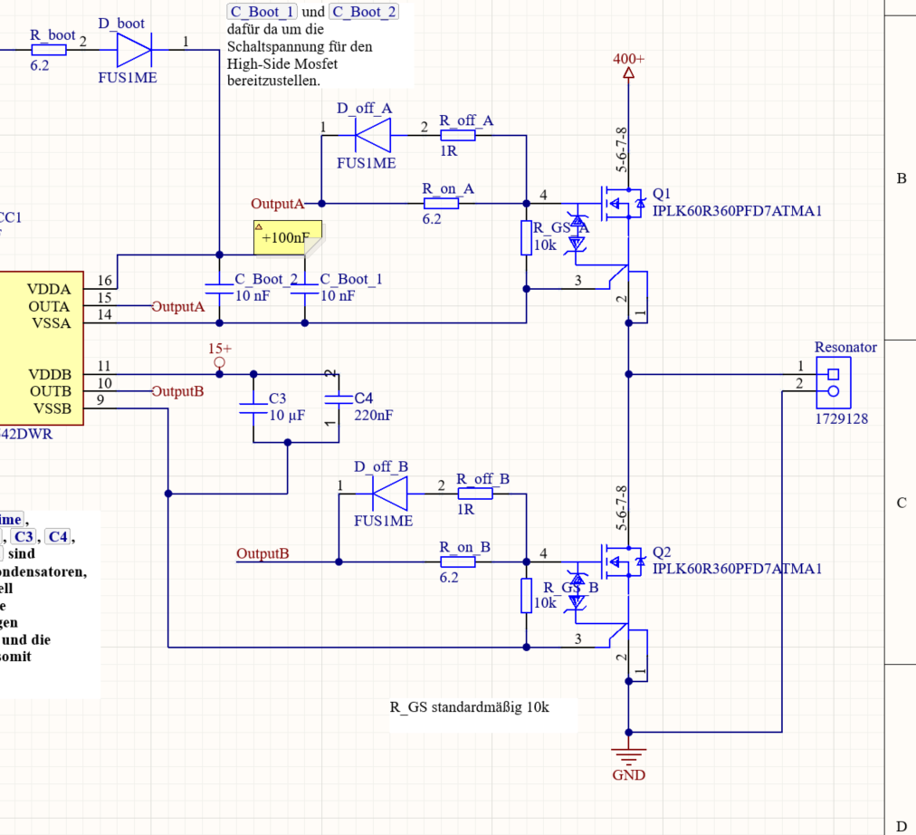
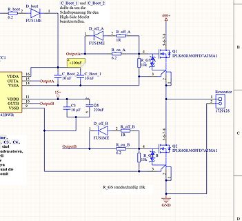
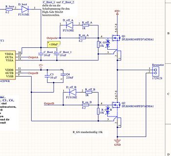
Mosfets. Im Oszillogram sieht man am obersten und untersten Channel die Spannung am Gate. Bei der High-Side ist eine Bootstrap vorhanden die das Potenzial am Gate auf 14,6 V über dem Potenzial an Source anhebt. Bei der Low-Side ist das Potenzial 15V gemessen gegen Ground. Rboot ist an die gleiche 15V
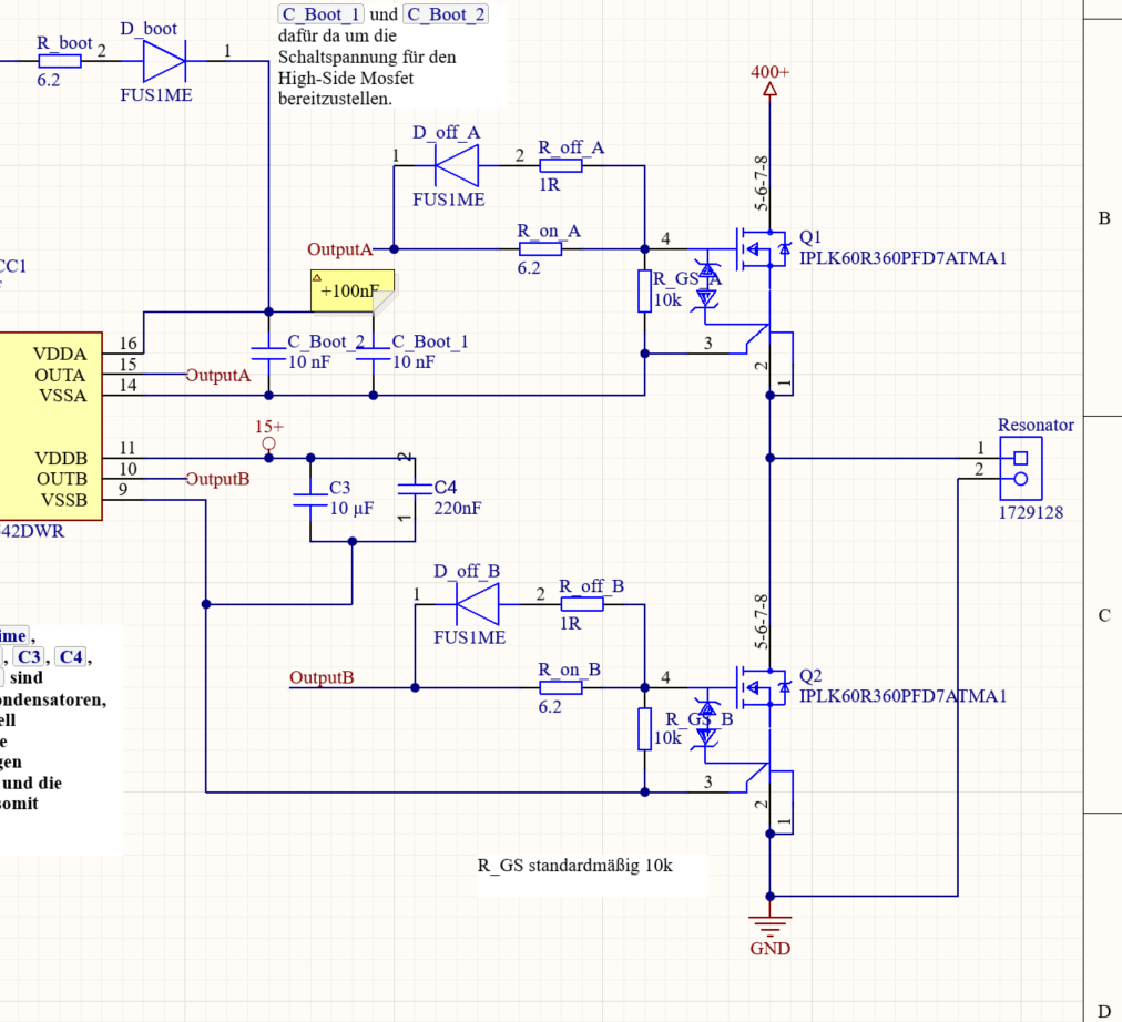
D boot, R boot, 6.2, 1, FUS1ME, C Boot_1, C Boot_2, dafür da um die Schaltspannung für den High-Side Mosfet bereitzustellen., 400+, OutputA, 16, VDDA, 15, 10 nF, 14, VSSA, C Boot_2, C Boot_1, 15+, 10 uF, C3, 220nF, C4, 100nF, OutputB, 11, VDDB, 10, OUTB, 9, VSSB, 2, R off A, 1R, FUS1ME, D off A, 6.2
D boot, R boot, 6.2, 1, FUS1ME, C Boot_1, C Boot_2, dafür da um die Schaltspannung für den High-Side Mosfet bereitzustellen., 400+, OutputA, 16, VDDA, 15, 10 nF, 14, VSSA, C Boot_2, C Boot_1, 15+, 10 uF, C3, 220nF, C4, 100nF, OutputB, 11, VDDB, 10, OUTB, 9, VSSB, 2, R off A, 1R, FUS1ME, D off A, 6.2
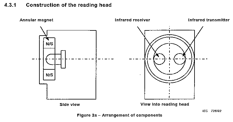
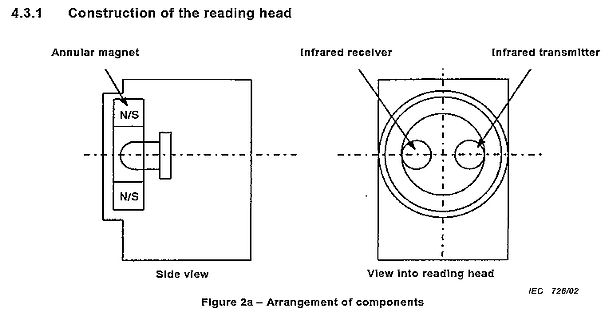
4.3.1 Construction of the reading head
Annular magnet
N/S
N/S
Infrared receiver
Infrared transmitter
Side view
View into reading head
IEC 726/02
Figure 2a – Arrangement of components
≤3 V Maximum open-circuit voltage during operation 30 V d.c. b) Power supply On the tariff device side the interface is passive. The HHU supplies the necessary power. c) Connections Via terminals or suitable connectors. Polarity errors can prevent communication, but shall not harm the devices. 62056-
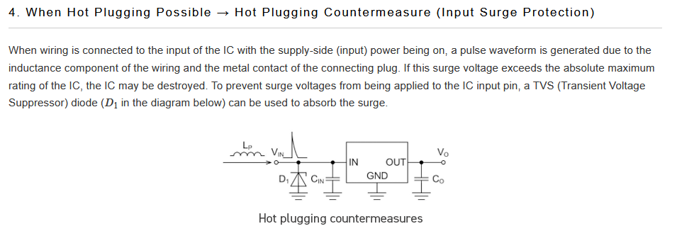
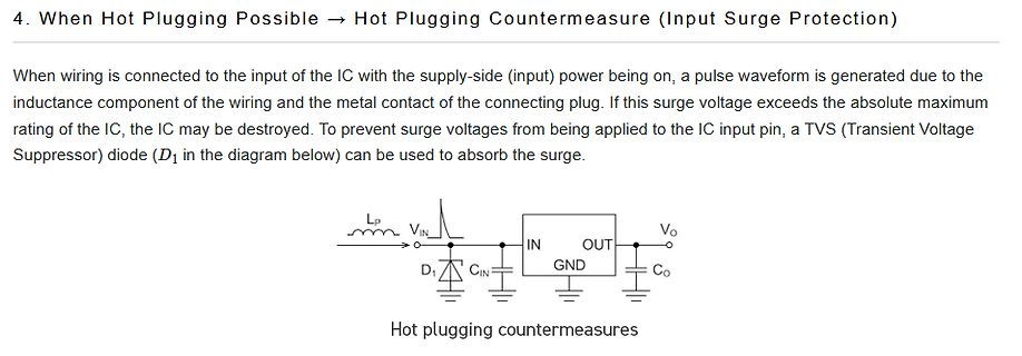
Countermeasure (Input Surge Protection)
When wiring is connected to the input of the IC with the supply-side (input) power being on, a pulse waveform is generated due to the inductance component of the wiring and the metal contact of the connecting plug. If this surge voltage exceeds the absolute maximum rating
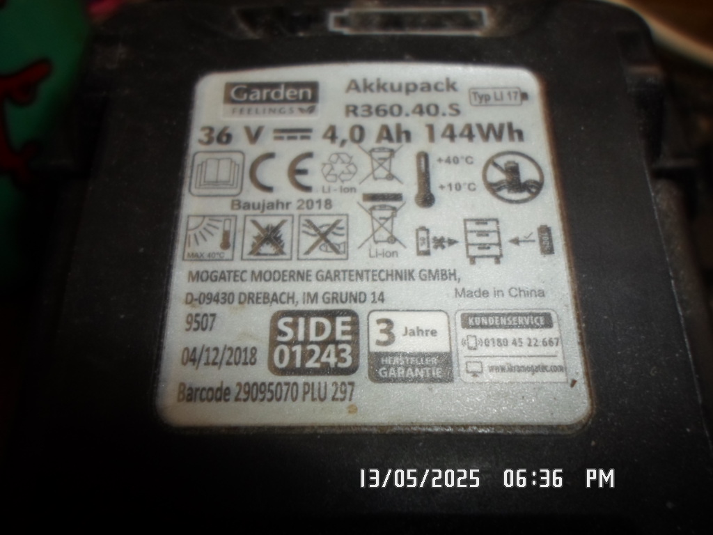
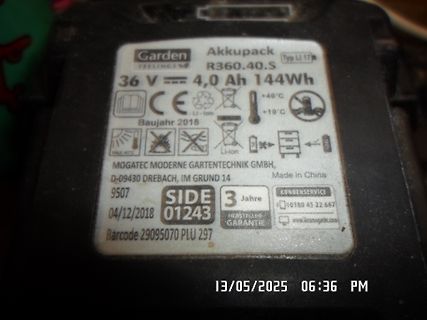
V 4,0 Ah 144Wh Baujahr 2018 MOGATEC MODERNE GARTENTECHNIK GMBH, D-09430 DREBACH, IM GRUND 14 9507 SIDE 01243 3 Jahre KUNDENSERVICE 04/12/2018 Barcode 29095070 PLU 297
T ist schaltbar auf 0 - 125 Volt und 125 - 250 Volt. In of the voltage switch located at the left side. The fuse of R diesen Bereichen läßt sich die Ausgangsspannung an this output is M 4A(for 3A-Version)other M6,3A(for 4,5A- der Ausgangssteckdose einstellen. Der Ausgang ist mit Version) and located
X 8 V. Examples Take TA612 as an example, connect TA612 through XCOM serial assistant on computer side, the connection parameters are baud rate 9600, 1 stop bit, 8 data bits, no parity. 1.Get device information Send hexadecimal data through XCOM:AA55 00 03 02. TA612 return: 55AA00 07 64 02 22 01 8F.
odklopte stranu s obrázkami a potom sa oboznámte so všetkými funkciami prístroja. Før du læser, vend siden med billeder frem og bliv bekendt med alle apparatets funktioner. Antes de empezar a leer abra la página que contiene las imágenes y, en seguida, familiarícese con todas las funciones del dispositivo
refer to "Handling Precaution for Terminals and Connectors"described on our website • Top entry but side feed type (Technical documents of Product infomation page). * Dimensional unit: mm • Connector for DC power supply * RoHS2 Compliance • Corresponding to sucking nozzle of pick * Contact JST for details
regulation is measured at the bottom of the package. R1 the value of resistor R1 in ohms Negative side sensing is a true Kelvin connection, with the At a Ripple frequency of 120Hz, with R1= 100 bottom of the output divider returned to the negative side of the 1 load. Although it may not be immediately
scheint es zu sein. W+, D, GND sind die adressierbaren LEDs W+,W- die warmweißen. Da wird die die Low-Side per PWM geschaltet. > Wobei der WS2812 nicht mit 12V läuft Die Pins des 8Pin-µC sind wie folgend beschalten 1. Taster - active-low 2. IR-input 3. Mic Input 0-5V, 2.5 bei Ruhe 4. GND 5. RGB-LED-Data 6. VCC 7. W- PWM (schaltet über FET Low-Side) 8. W+ schaltet über FET 12V der LEDs an/ab
may have a vast range, depending on the used MOS-FET, e.g. down to 2 Volt at the “Lower voltage” side and up to 10 Volt or more at the “Higher voltage” side of the level shifter. An additional function of the level shifter is that it can isolate a powered-down section in a bus system, without obstructing
you have the vertical switches then the side with the metal indent should face to the outside edge of the board. Side mount switches should have the switch lever towards the middle of the board. Ensure the switches are flush with the board and
Maintenance Battery tray removal on rack models A - emove the front panel. B - emove the left-hand side of the A B front panel by pushing the button and then by sliding the part. C - isconnect the battery block by separating the two connectors (never pull on the wires). C D - emove the metal protection
Schaltspitzen, ...): -https://www.infineon.com/cms/de/product/power/smart-power-switches/high-side-switches/power-profet-plus-12v-automotive-smart-high-side-switch/ Und da steht dann: [pre] The ability to drive high current loads makes Power PROFET™ very well adapted to replace electromechanical
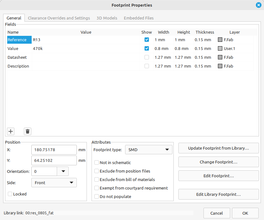
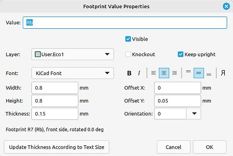
0 mm
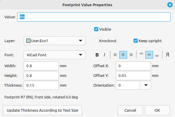
Height: 0.8 mm
Offset Y: 0.05 mm
Thickness: 0.15 mm
Orientation: 0
Footprint R7 (Rb), front side, rotated 0.0 deg
Update Thickness According to Text Size
Cancel
OK
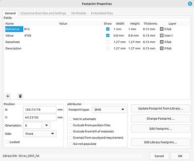
Description 1.27 mm 1.27 mm 0.15 mm F.Fab
Position
X: 180.75178 mm
Y: 64.25102 mm
Orientation: 0
Side: Front
Attributes
Footprint type: SMD
Not in schematic
Exclude from position files
Exclude from bill of materials
Exempt from courtyard requirement
Do not populate
Update Footprint from Library...
Change
choice of double crimp n Double crimp connections can be or single wires. The two wire drives produced side-by-side or one above are fitted with highly dynamic AC-servo the other axes and an integrated anti-slip system. n Integrated head separation and batch With this sophisticated handling technology, two
Hex Operation necting all of the V pins to a common pad located on both D7 D6 D5 D4 D3 D2 D1 D0 CC sides of the PC board. This technique offers a low thermal Lamp Test resistance for IC to system ambient. 1 1 1 1 0 B B B (OFF) ESD Protection Lamp Test 1 1 1 1 1 0 0 0 F8 The input protection structure
Neben den bereits genannten Vorschlägen (Optokoppler unnötig, High-Side-Switch) kann ich nur empfehlen alle GND-Pins des RasPi Picos auch mit der Masse Deiner Platine zu verbinden und nicht nur einen wie im Schaltplan gezeigt. Der R-78CK-0.5 Spannungsregler sollte noch
meter height for 1 cycle, 2 drops from No temperature rising each cell terminal and 1drop from the side of cell can (Total number of drops = 3). 4.4.2 Cells charged per 4.1.1 are vibrated for 90 minutes per No leakage Vibration Test each of the three mutually perpendicular axis (x, y, z) with total excursion
P ico 2 W, as well as support for PSRAM with size autodetection. The PIO interface now supports side_pindir selection, and SPI allows the MISO pin to be unspecified. Both the I2C and SPI classes now have the bus identifier as an optional argument with a default based on the board configuration. WPA3
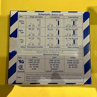
Form A or 1 Form B Contact capacity 20 W (high contact pressure) 5 to 15 W Operating function Single side stable Single side stable Latching “Getter” hole Yes No 155 R REFERENCE DATA 1.-(1) Contact reliability 1.-(2) Contact reliability 2. Coil temperature rise (under saturated Test sample: R-SD-24V 54
Wenn du die Lüfter low-side schaltest, dann funktioniert der Tachoausgang nicht mehr.
mit N-Channel FET? Brauchst du hier nicht fragen. Lerne selbst: Suchst du nach "mosfet high side switch mikrocontroller.net" und findest ein paar erleuchtende Beiträge/Threads.
15 ns Fall time (output) tKFP 15 ns a) Refer to 2.3 “Port current”. b) Do not exceed 30mA per each side of microcontroller. R01DS0145EJ0102 28 Data Sheet Chapter 5 I/Ospecification 5.1.3 PgE1 Table 5-6 PgE1 characteristics Parameter Symbol Condition Ratings Unit Min Typ Max - - - Schmitt1 0.7·E1VDD E1VDD
Nicht-Benutzung der Taster-Anschlüsse der ADC überhaupt nicht) benötigt wird. Anmerkung zu Q2…Q6. Die Low-Side-Treiber des LED-Displays Q2 bis Q6 arbeiten in Kollektorschaltung. Dies bietet zwei Vorteile: Zum einen können die Transistoren dadurch nicht in Sättigung geraten, zum anderen entfallen gegenüber der
ich: Q3 & Q6 … was Q7 macht ist mir unklar. An weiß fällt es mir schwer. Q5 hatte ich als High side, die low side verstehe ich aber nicht Vllt kannst du uns ja auch inhaltlich erhellen. ^^ habe ja viel Respekt vor deine Expertise, aber dass du dir immer erst die Eier kraulen lassen musst verstehe
is mounted on the pins of the current lead-in on the compressor. the compressor. At first the left side is mounted, then theof right side is pressed over the screw on the bracket (sideways, marked in grey).The electronic unit snaps on to the bracket and is now securely mounted on the compressor. Earth
output type 11.±0.5 . Ip K 0 3 TVS L 22±0.5 Voltage output type 23.5±0.5 Schematic diagram Front View Side View 35.3 Three-core plug size X Y LOutput VacancyK Output 2.5mmAudio Plug 11.9 2.5 Optional ΦY standard 3.5mmAudio Plug 15.0 3.5 1m X Diagram for standard three-core plug Table of technical parameter
in a write to the temporary (TEMP) register instead of the low byte register, as shown in the left side of Figure 8-6. When the high byte register of the 16-bit register is written, TEMP will be copied into the low byte of the 16-bit register in the same clock cycle, as shown in the right side of Figure
so gesehen: > > VCC > | > Last > | > Shunt > | > Gnd Das nennt sich dann "low side"-Messung, bei dir ist es eine "high side"-Messung. Low side ist einfacher umzusetzen. Prinzipiell funktioniert das, auch mit Verstärkung 3000. In einem OpAmp wird das schwer, setz das lieber
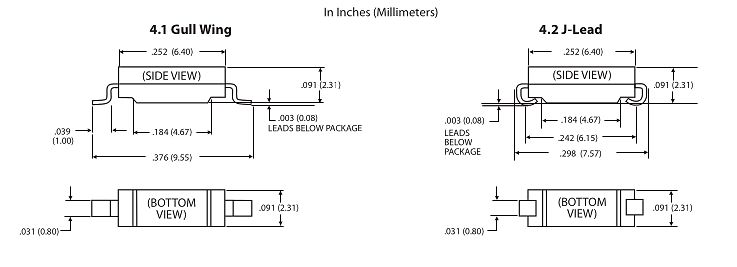
Package dimensions exclude molding flash. 2.70 8. The end flash shall not exceed 0.127 mm on each side of package. 0.10 9. Tolerance is +/- 0.254 mm unless otherwise 1.55 0.00 0.70 1.00 specified. 1.45 For more information, please contact: Melexis, Inc. 41 Locke Road Concord, NH 03301 Phone: (603) 223
Technologies to assure a smooth and well executed transition. If Infineon does not hear from your side by the due date, we will assume your full acceptance to this proposed change and its implementation. Your attention and response to this matter is greatly appreciated. Infineon Technologies AG Postal

 Bild
Bild
 Bild
Bild
 Bild
Bild
 Bild
Bild
 Bild
Bild
 Bild
Bild
 Bild
Bild
 Bild
Bild
 Bild
Bild
 Bild
Bild
 Bild
Bild
 Bild
Bild
 Bild
Bild
 Bild
Bild