LED Lampen und ESL darf es bei weitem nicht so heiß werden. Solange man in einer Lampe die für eine max. 60 W Glühlample vorgesehen war auch nur eine 7 W LED Lampe rein macht die ähnlich hell ist, hat man eher noch kein Problem. Die 15 W LED Lampe hat aber ggf. schon ein Hitzeproblem - zumal die Typen
montieren. Z.B. noch billiger und noch heller: https://www.pollin.de/p/led-deckenleuchte-v-tac-vt-8-10-660-eek-a-10w-1200-lm-300-mm-4000-k-535670 10W, 1200 lm, 4000 K für 4,95€
Common Common Raw Emitted Length Vf(V)20mA Iv(ucd)10mA Fig.No. Cathode Anode Material Color ɡp(nm) Typ. Max. Typ. C-574H A-574H GaP Red 700 2.3 2.8 700 C-574E A-574E GaAsP/GaP Hi.effi Red 635 2.1 2.8 2000 C-574G A-574G GaP Green 565 2.1 2.8 2000 D53 C-574Y A-574Y GaAsP/GaP Yellow 585 2.1 2.8 1600 C-574SR A-574SR GaAlAs Super Red 660 1.8 2.2 21000 Fig. D53 1.All dimension are in millimeters (inches). 2.Tolerance is Ô 0.25 mm (0.01") unless otherwise specified. E-34
Sinking Current operation with a full set of specifications at 5V. ■ Guaranteed Offset Voltage: 50µV Max Specifications at ±15V are also provided. ■ Guaranteed Low Drift: 1.3µV/°C Max The LT1006 has a low offset voltage of 20µV, drift of ■ Guaranteed Offset Current: 0.5nA Max 0.2µV/°C, offset current of
proof to battery and ground • Thermally protected. QUICK REFERENCE DATA SYMBOL PARAMETER MIN. TYP. MAX. UNIT VBAT supply voltage on pin BAT 5 12 27 V BAT supply current on pin BAT in sleep mode 1 3 8 A supply current on pin BAT in standby mode; bus recessive 100 400 1000 A supply current on pin BAT in
Electrical Characteristics Standard value Display Format 128 X 64 DOTS ITEM Symbol Condition UNIT Min. Typ. Max. Drive Method 1/64 Duty ; 1/9 Bias Supply Voltage For Logic V DD SS -- 4.5 5.0 5.5 V Supply Voltage For LCD VDDV 0 -- -- 9.0 -- V LCD Type STN/Transflective/positive Y/G Input High Voltage V -- 0.7V
Electrical Characteristics Standard value Display Format 128 X 64 DOTS ITEM Symbol Condition UNIT Min. Typ. Max. Drive Method 1/64 Duty ; 1/9 Bias Supply Voltage For Logic V DD SS -- 4.5 5.0 5.5 V Supply Voltage For LCD VDDV 0 -- -- 9.0 -- V LCD Type STN/Transflective/positive Y/G Input High Voltage V -- 0.7V
Electrical Characteristics Standard value Display Format 128 X 64 DOTS ITEM Symbol Condition UNIT Min. Typ. Max. Drive Method 1/64 Duty ; 1/9 Bias Supply Voltage For Logic V DD SS -- 4.5 5.0 5.5 V Supply Voltage For LCD VDDV 0 -- -- 9.0 -- V LCD Type STN/Transflective/positive Y/G Input High Voltage V -- 0.7V
Electrical Characteristics Standard value Display Format 128 X 64 DOTS ITEM Symbol Condition UNIT Min. Typ. Max. Drive Method 1/64 Duty ; 1/9 Bias Supply Voltage For Logic V DD SS -- 4.5 5.0 5.5 V Supply Voltage For LCD VDDV 0 -- -- 9.0 -- V LCD Type STN/Transflective/positive Y/G Input High Voltage V -- 0.7V
Electrical Characteristics Standard value Display Format 128 X 64 DOTS ITEM Symbol Condition UNIT Min. Typ. Max. Drive Method 1/64 Duty ; 1/9 Bias Supply Voltage For Logic V DD SS -- 4.5 5.0 5.5 V Supply Voltage For LCD VDDV 0 -- -- 9.0 -- V LCD Type STN/Transflective/positive Y/G Input High Voltage V -- 0.7V
. 7-S23-1 Internal Circuit Diagram Selection Guide Iv (ucd) @ 10 mA Part No. Dice Description Min. Max. SA23-11HWA SA23-12HWA Common Anode, Rt. Hand Decimal BRIGHT RED (GaP) 900 2200 SC23-11HWA Common Cathode, Rt. Hand Decimal SC23-12HWA SA23-11EWA SA23-12EWA Common Anode, Rt. Hand Decimal HIGH EFFICIENCY
140 - - mA Drain-source on-state resistance R DS(on) V GS=0 V, ID=70 mA - 1.7 3.5 Ω V GS=10 V, ID=660 mA - 1.0 1.8 |V |>2|I |R , Transconductance g fs DS D DS(on)max 0.4 0.8 - S ID=0.48 A 3) Threshold voltage V GS(th)orted in bands J V GS(th) V DS=3 V, ID=108 µA -1.2 - -1 V K -1.35 - -1.15 L -1.5 -
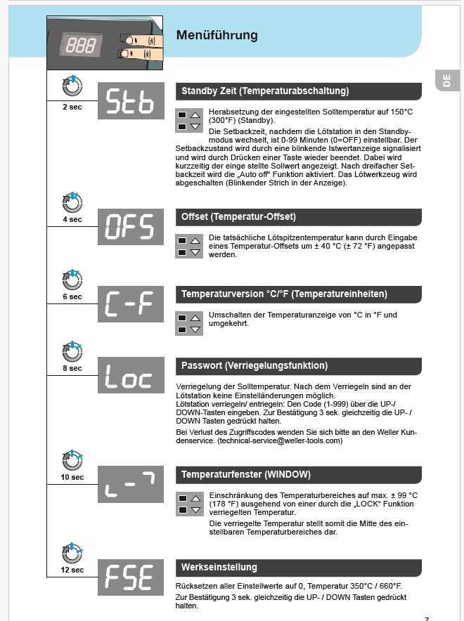
technical-service@weller-tools.com)
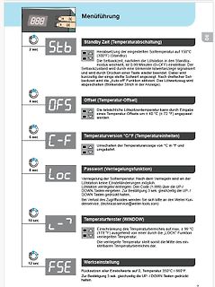
L- Temperaturfenster (WINDOW)
10 sec
Einschränkung des Temperaturbereiches auf max. ± 99 °C (178 °F) ausgehend von einer durch die „LOCK“ Funktion verriegelten Temperatur.
Die verriegelte Temperatur stellt somit die Mitte des einstellbaren Temperaturbereiches dar.
FSE Werkseinstellung
12 sec
Rücksetzen aller Einstellwerte auf 0, Temperatur 350°C / 660°F. Zur Bestätigung 3 sek. gleichzeitig die UP-/DOWN-Tasten gedrückt halten.
erreichen und das war "viel Eisen". Nö. Den Modulationstrafo brauchte man nur bei AM und da waren max 4,5kHz erlaubt (9kHz Frequenzraster).
und das war "viel Eisen". > > Nö. > Den Modulationstrafo brauchte man nur bei AM und da waren max 4,5kHz > erlaubt (9kHz Frequenzraster). ..und was war möglich? Gruß, Holm
Max S. schrieb im Beitrag #4790508: > Was bringen Standards wenn aber nicht jeder Compiler sie nutzt?!? Umgekehrt: Was nutzt ein Compiler, der keinem Standard folgt?
überwiegenden Mehrheit der für den PC benutzten Pascaldialekte diesen speziellen Schalter. Das von Max genannte AVRco-Pascal ist da eine Ausnahme. Zeno
einigen Stunden LEDs anfingen auszufallen, wesentlich dunkler wurden und einige so hell, das man ihnen max. noch 5min. zutraut (NEIN, nicht konstruktionsbedingt durch def. der anderer LEDs!). Die leuchten bis heute noch... :) PS: Ne nix belichtensdingens, andre Spielerei.
michael_ schrieb im Beitrag #5530713: > Was machst du da für Platinen? Folien für A4 sind max. 29cm lang und da > geht auch noch der Rand ab. Na und? Da bekommt man locker 35cm lange Layouts drauf.
Da kann man dann gleich sich ein passendes Regime ausdenken: - 2..5 ms warten - TE messen - 0 .. max. 20 ms Heizer einschalten. Konkrete Dauer aus Berechnung des Heizbedarfes. - dann wieder dasselbe immer wieder immerhin würden die vollen 144 Watt ausreichen, den Kolben binnen weniger Sekunden zur
. 24V wirst du schon brauchen, aber mit Strombgrenzung. Wie viel schafft so eine 245 Spitze max? 10A sind für eine normale Platine imho zu viel. Ich plane es mit max 100W zu betreiben.
Electrical/Optical Characteristics at Ta=25 LTS-4705/4710/4730/4740/4780AWC Parameter Symbol Min. Typ. Max. Unit Tset Condition 200 650 IF=1mA Average Luminous Intensity IV cd 3100 IF=5mA Peak Emission Wavelength P 660 nm F=20mA Spectral Line Half-Width 35 nm F=20mA Dominant Wavelength d 638 nm F=20mA 1.6
daß ein „normaler“ Drehstromgenerator erheblich mehr Leistung erzeugen kann als z.B. 55A x 12Volt = 660 Watt. Der Regler begrenzt die Ausgangsspannung auf z.B. 14Volt damit das Bordnetz nicht explodiert. Läßt man denselben Generator aber mit maximaler Erregung laufen, produziert er leicht 55A x 40Volt
maximalen Ladeleistung meiner Lichmaschine ist. Bei moderater Langstreckengeschwindigkeit (2/3 der max Drehzahl), bekomme ich schon lange die volle Leistung aus der LiMa, was ohne Booster nicht der Fall wäre. Die Lichtmaschine muss temperaturüberwacht werden, weil bei der geringeren Spannung erheblich
Kit8 o.ä.) nehmen. Das Programm mit JSON Erweiterung raufspielen. Lesekopf basteln (geht auch ohne MAX485). Den Kollektor per Widerstandsteiler (wegen Pegelwandlung auf 3,3V) an RxD anschließen. Bei einigen Modulen ist der Serial0 durch USB-Anschluss belegt, dann in der Setup-Routine folgenden Code nach
auf die Geschwindigkeit der optischen Sonde zu setzen. Die Wellenlänge des Schnittstelle beträgt 660 nm, die Lichtstärke im aktiven Zustand ist minimal 1 mW/sr. Vielleicht kann Peter was dazu sagen, ob sein Code das Lesen/Dekodieren kann. Hab mich mit dem Code noch nicht intensiv beschäftigt.
Symbol Parameter TA= 25°C -40 to 85°C -55 to 125°C Unit VI VO |O | V DD (V) (V) ( A) (V) Min. Typ. Max. Min. Max. Min. Max. IL Quiescent Current 0/5 5 0.04 5 150 150 0/10 10 0.04 10 300 300 A 0/15 15 0.04 20 600 600 0/20 20 0.08 100 3000 3000 VOH High Level Output 0/5 5 4.95 4.95 4.95 Voltage 0/10 10
beispielsweise in seinem initialen Post mit einem ungeprüften Eingangswert verwendet. Da könnte auch mal SIZE_MAX drinstehen. Ja, das nenne ich schlampig. Jetzt könnte man noch drüber philosophieren, was - wenn dieser Eingangswert geprüft werden soll - wohl ein sinnvoller Wert wäre, gegen den man da prüft
LMC662C Parameter Test Conditions Typ Limit(1) Limit(1) Units Input Offset Voltage 1 3 6 mV 3.3 6.3 max Input Offset Voltage 1.3 μV/°C Average Drift Input Bias Current 0.002 pA 4 2 max Input Offset Current 0.001 pA 2 1 max Input Resistance >1 TeraΩ Common Mode 0V ≤ VCM ≤ 12.0V 83 70 63 dB + Rejection
bemühen, um mal nachzurechnen. hab ich getan ein Monokristallines Solarmodul der Spitzenklasse 660mm x 1483mm ~ 1m^2 bringt max 120Wp das ergibt eine installierte Leistung von 3,6KWp bei 30 m^2 bei 186 Tagen und 8h Sonne 1488 Sonnenstunden/a. 1488h/a * 3,6KW = 5356,8 KWh/a kann mich auch verrechnet
=25 LTS-4301WC/4801WC/LTD-4608WC/4708WC/LTC-4624WC/4724WC/4627WC/4727WC Parameter Symbol Min. Typ. Max. Unit Tset Condition 200 650 F=1mA Average Luminous Intensity IV 3400 cd F=5mA Peak Emission Wavelength P 660 nm IF=20mA Spectral Line Half-Width 35 nm IF=20mA Dominant Wavelength d 638 nm IF=20mA 1.6
Leistungszulage, ERA10b-11a; FH-Abschluss ERA10a). Nach 4 Jahren liegt man bei ca. 4900.-. Den vollen Bezug (max. 15,5 Monatsgehälter) gibt es nach 6 Jahren. Bei 5400.- ist dann das obere Ende als "normaler" Ingenieur erstmals erreicht, alles Weitere ist außertariflich, was aber nur sehr schwer erreichbar ist.
im ersten Jahr voll bekommt. Zusätzlich kommt dann noch die Gewinnbeteilung hinzu - die bis zu max. 157 Prozent betragen kann - wurde bei diesem Wert eingefroren. Denke im Jahr 2011 sollte da mind. das 1,5 fache Monatsgehalt drinnen sein. Übrigens mein Einstiegsgehalt nach der Lehrzeit 2004
Seating Plane) 260°C for 3 Sec Electrical / Optical Characteristic @ Ta=25°C Parameter Symbol Min. Typ. Max. Unit Test Condition Grade Dominant Wavelength λd 660 nm IF=20mA Spectral Line Half-Width △λ 20 nm I =20mA F Forward Voltage V F 1.7 1.8 2.0 V IF=20mA Reverse Current R 20 μA V R5V Luminous Intensity
@Betrachter: Als realistisch würde ich ein Gehalt zwischen 35000€ und max. 70000€ sehen, je nach Berufserfahrung, Abschluss und Arbeitsort.. In München wird man als Ingenieur die 60000€ wahrscheinlich leichter erreichen als in einer anderen Stadt. Wenn man aber bedenkt,
Entwicklungsingenieur Region: Baden Württemberg ist das gerecht nur so eine frage? Gruss, Max
mA - 700 - I = 100 mA, I = 5 mA - 900 - C B Base-emitter voltage 1) VBE(ON) C = 2 mA, VCE= 5 V 580 660 700 I = 10 mA, V = 5 V - - 770 C CE 1) Pulse test: t < 300 s; D < 2% Semiconductor Group 2 May-12-1998 BC 847S Electrical Characteristicsat A =25°C, unless otherwise specified Parameter Symbol Values Unit min. typ. max. AC Characteristics per Transistor Transition frequency f - 250 - MHz T IC= 20 mA, V CE = 5 V, f = 100 MHz Collector-base capacitance C cb - 2 - pF V = 10 V, f = 1 MHz CB Emitter-base capacitance C
Bemessungswerte / Ratings: I - t Verhalten / I - t characteristics: N N BC_AC / 2 Art. No. I U N_AC / DC U d_max P d_max I t Bemessungs- Schmelzzeit N [V] [mV] [W] DC [A s] [A] strom-Faktor / 520.602 2) 32 mA 250 / 60 10.000 1,6 35 / 0,32 0,00008 / Melting time: 2) Rated current 520.603 40 mA 250 / 60 8.000 1,6
min. typ. mall. Unit Standby input eurrent 10 <1 10 ~A Supply eurrent with open output Iso 20 35 mA Max. output power at 8 Q (tone 3) Pa 0.16 W Max. output voltage atQ (tone 3) VQ pp 2.8 4.0 V Deviation 01the max. individual amplitudes relerred to tone 3 LVQM ± 5 °/0 Frequeney variation 01 basic oscillator
min. typ. mall. Unit Standby input eurrent 10 <1 10 ~A Supply eurrent with open output Iso 20 35 mA Max. output power at 8 Q (tone 3) Pa 0.16 W Max. output voltage atQ (tone 3) VQ pp 2.8 4.0 V Deviation 01the max. individual amplitudes relerred to tone 3 LVQM ± 5 °/0 Frequeney variation 01 basic oscillator
dissipation for a single output R qJA + R qJC ) R qCS ) R qSA (eq. 5) regulator (Figure 28) is: where: PD(max) + [V I(max)* V Q(min) Q(max) ) R qJC is the junction-to-case thermal resistance, )V I (eq. 3) I(max) q R qCS is the case-to-heatsink thermal resistance, where: R qSA is the heatsink-to-ambient thermal
specification and ordering codes Characteristics (T = 85 °C) A Ordering code Type V RMS V DC imax W max P max 8/20 µs 2 ms (1 time) (1 time) V V A J W T14 V RMS= 130 … 420 V B72214T2131K105 T14K130E2 130 170 6000 50 0.6 B72214T2151K105 T14K150E2 150 200 6000 60 0.6 B72214T2171K105 T14K175E2 175 225 6000
Personalverantwortung, Tarif an IG-Metall angelehnt Tendenz: näxte Jahre wird's effektiv weniger, max. 0,5% jährliche Lohnanhebung (soweit ich weiß, Inflationsrate ist höher) Kumpel: bei T-elekom T-ochter beschäftigt, 40 Std., nicht studiert, nur Handwerkslehre, seit Jahren auf Ingenieursposten
Applikationsingenieur keine B.E. 1. Jahr 44k (mit 6 Monaten Probezeit) ab 2. Jahr 47k + Bonus max. 20%
-1 Package Dimensions Internal Circuit Diagram Selection Guide Iv (ucd) Part No. Dice @ 10 mA Min. Max. Description SA08-12HWA Common Anode, Lt Hand Decimal SA08-13HWA Common Anode, Rt & Lt Hand Decimal SA08-21HWA Common Anode, Rt Hand Decimal BRIGHT RED (GaP) 360 1400 SC08-11HWA Common Cathode Rt. Hand
Characteristics , atTj= 25 °C, unless otherwise specified Parameter Symbol Conditions Values Unit min. typ. max. Characteristics Transconductance g V ≥2*I *R , - 12 - S fs DS D DS(on)max D =13A Input capacitance C iss VGS =0V, DS =25V, - 3000 - pF Output capacitance C oss f=1MHz - 1170 - Reverse transfer capacitance

 Bild
Bild
 Bild
Bild
 Bild
Bild