off command D iplay on 3. Initialization VCC 4. Clear Screen 5. Power up V CC VDDVBAT 6. Delay 100ms SS/Ground (When V CC is stable) 7. Send Display on command Display off 4.2.2 Power down Sequence: V CC/ VBATff 1. Send Display off command VDDoff 2. Power down V CC / VBAT VCCVBAT 3. Delay 100ms (When
er nicht mehr mit Multiplikation und Division klar. Richtig ist: bei einer Abtastung von 1000 ms _geteilt durch_ 1 [math]\frac{5+5+5(W)}{1(\frac{1}{s})}=15(Ws)[/math] bei einer Abtastung von 250 ms _geteilt durch_ 4 Alexander schrieb im Beitrag #7621664: > Εrnst B. schrieb im Beitrag #7618905
Jiha, 15:51 ist ne Palindromzeit. Na schaffst du wenigstens noch ne volle Stunde? Wo du schon das Thema Zeit aufbringst
LU90614 ? Hier ist ein Beispiel in C mit dem LU90614 an einem STC12C5A60S2 (8051 CPU) http://www.51hei.com/bbs/dpj-225613-1.html Daraus würde ich es so interpretieren dass "T" der Receiver des LU90614 ist und an "Tx" des Mikrocontroller angeschlossen werden muss. Das Bild im Anhang mit den Pins
10 00 00 00 00 chk:B8==B8 LU90614.read() AMB:0.16 'C - eine Werte-Abfrage kann nur ca. alle 500ms erfolgen! (die Abfrage von 1000 gueltigen Werten dauert 505 sec !) - bei Betrieb mit 5.0 V an Vin wird das Board selbst sehr warm - im "Body"-Modus sind werte unter 36 Grad ungueltig! Hi=FF Lo
VR 2.3 2.6 2.9 V AC Characteristics ● Internal timing parameters PDisplay scan cycle TTPR 40 85 20 ms Key scan interval T KS 20 40 80 ms ●Interface timing parameters DIO falling edge of the start signal setup timTSSTA 100 - - ns DIO falling edge of the start signal hold timT HSTA 100 - - ns DDIO rising
Bürstadt mit konzeptgemäßer Fehlerklärung Stromkreises nach Wehrendorf mit konzeptgemäßer nach 150 ms und Freischaltung der Sammelschiene. Fehlerklärung nach 150 ms. Langfristanalyse 2030 (V2022) - Executiv01.09.202338 Übersicht der Wirkung untersuchter Sensitivitäten Gegenmaßnahme Wirksamkeit Erhöhung
voltage negative between 10% to 95% during ramp up AC ramp up 1.5 s Start-up Time PS_On activated 150 ms -52V Ramp 1A/ms ±2080 Transient Response 12Vsb Ramp 1A/ms ±600 mV Current sharing accuracy (up to 3 in parallel) At 100% load ±10 % Hot Swap Transients All outputs within regulation Hold-up Time 15 19 ms GENERAL CHARACTERISTICS Parameter Conditions Min. Typ. Max. Units Storage Temperature Range Non-condensing -40 70 Operating Temperature Range 0 50 °C Operating Humidity Non-condensing 10 90 % Storage
Watchdog Oscillator Cycles Typ Time-out (V = 5.0V) Typ Time-out (V = 3.0V) Number of Cycles CC CC 0 ms 0 ms 0 4.1 ms 4.3 ms 512 65 ms 69 ms 8K (8,192) Main purpose of the delay is to keep the AVR in reset until it is supplied with minimum Vcc. The delay will not monitor the actual voltage and it will
temp cpi alt_flag, 0 brne alt_2flash ;flash LED 1 time sbi DDRB, PB2 ;turn IR LED on rcall delay15ms cbi DDRB, PB2 ;turn IR LED off rjmp alt_exit ;flash LED 2 times alt_2flash: sbi DDRB, PB2 ;turn IR LED on rcall delay15ms cbi DDRB, PB2 ;turn IR LED off rcall delay100ms rcall delay100ms sbi DDRB, PB2 ;turn IR LED on rcall delay15ms cbi DDRB, PB2 ;turn IR LED off alt_exit: rcall delay100ms rcall delay100ms rcall delay100ms rcall delay100ms rjmp int_exit keyin: andi key, 0b00111111 ;mask alt-key out rcall getkey ;decode key and send
div. V 2V/div. OUT 2V/div. IL IL 1A/div. 2A/div. IL 2A/div. VSW VSW 10V/div. 10V/div. VSW 10V/div. 2ms/div. 2ms/div. MP2307-TP04 MP2307-TPC05 MP2307-TPC06 Load Transient Test Short Circuit Test Short Circuit Recovery Waveforms Waveforms Waveforms V IN= 12V, VOUT = 3.3V, IOUT = 1A to 2A step VIN= 12V,
OUT 2V/div. 2V/div. 2V/div. VSW VSW V SW 10V/div. 10V/div. 10V/div. IL IL L 1A/div. 1A/div. 1A/div. 5ms/div. 1ms/div. 5ms/div. Shutdown Startup Shutdown IOUT = 1A IOUT = 2A IOUT = 2A V V VEN 5V/div. 5V/div. 5V/div. VOUT VOUT VOUT 2V/div. 2V/div. 2V/div. V VSW V SW SW 10V/div. 10V/div. 10V/div. L L L 1A
Simulationsbilder unter dem Schaltplan zeigen nur Ausschnitte aus der Gesamtsimulation, die sich ja über 50ms erstreckt.
Kelvinklemmen da doch die bessere Wahl. Dennoch kann man das gut über den Strom messen. Wenn ich den Fet für 3ms einschalte, dann messe ich ~6A, bei einem intakten Magneten kommen. Den Maximalstrom erreicht der Magnet nach ~75ms, mit etwas über 59A. Bei einem Kurzschluss messe ich nach 3ms aber schon ~20A Wenn
RAND and the secret individual subscriber key K. i RES is returned via the MS across the radio link to the SN which checks that XRES = RES to authenticate the subscriber. The SIM also sends cipher key CK to the MS. After successful subscriber authentication, the encrypted radio
" diese Markierung heraus, bleibt sie auch für die Person, die die Mail bekommt, sichtbar. 4.1: MS Paint (für mich relevant für meine einfachen Grafiken, arbeite SEHR viel mit Paint) ist mehr oder weniger unbenutzbar. a) Während ich in MS Paint einen Text schreibe, markiert Windows plötzlich völlig
Sun-Systeme genutzt. Aber auch hier könnte ich mir vorstellen, das es da mit der Kompatibilität zu MS nicht so weit her war.
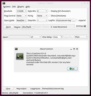
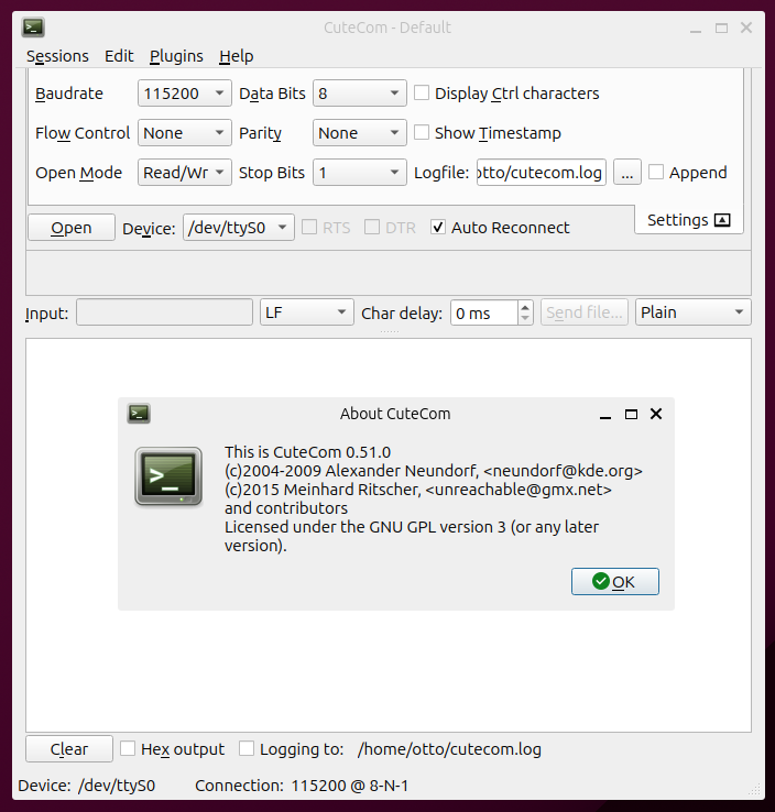
cutecom.log
Append
Open Device: /dev/ttyS0
RTS DTR Auto Reconnect
Settings
Input: LF
Char delay: 0 ms
Send file... Plain
About CuteCom 0.51.0
(c)2004-2009 Alexander Neundorf, <neundorf@kde.org>
(c)2015 Meinhard Ritscher, <unreachable@gmx.net>
and contributors
Licensed under the GNU GPL version 3 (or
^3ms waren gemeint. Also bei 1000mm/Tag = 500 U (2mm /U) sind das 500 x 2000 x 0,003s = 3000s 0,833h *0,165A = 0,137Ah /Tag. Wie gesagt, hier mit 5V gerechnet Bei 3V ziehen die Spulen weniger
aller günstigste Lösung sein, eben halbwegs im Rahmen. Daniel D. schrieb im Beitrag #7592828: > ^3ms waren gemeint. > > Also bei 1000mm/Tag = 500 U (2mm /U) sind das 500 x 2000 x 0,003s = > 3000s > > 0,833h *0,165A = 0,137Ah /Tag. > > Wie gesagt, hier mit 5V gerechnet > > Bei 3V ziehen
1.1 Vd Dropout voltage IO = 500 mA 1.05 1.15 V IO= 800 mA 1.10 1.2 Thermal regulation Ta= 25 °C, 30 ms Pulse 0.01 0.1 %/W 10/41 Doc ID 2572 Rev 31 LD1117xx Electrical characteristics Refer to the test circuits,JT = 0 to 125 °C, O = 10 µF, unless otherwise specified. Table 6. Electrical characteristics
Solange die Buslast rel. gering bleibt kommt eh so gut wie alles im 1.Versuch an. Und wenn es ne wenige ms später wird spielt bei dem was du vorhast keine Rolle.
oems":1536181272,"Tim":"2024012201234203","AuT":8.5,"KeT":50.9,"SpT":49.3,"AuI":8.3,"AuG":7.5,"KeI":51.0,"SpI":49.4,"MaT":170.5,"BrU":0,"BrE":0,"W1A":3,"Sp1":0,"Py1":0,"Fr1":255,"SpS":50,"ci":3} [/code] Solche Nachrichten brauchen dann schon einige CAN-Frames. Aber der volle Status wird pro Knoten
channeL. During hoLd operation, the underrange or overrange message can be polled by the Interface 3 ms after applying a measuring vaLue.0n caLling the internaL calibraEion program, accurate triangular signals (constant currents at approx. 70 Hz) are appLied to the transformer outputs, correcting values
Presence R Subwoofer Test Tone [Off] / On Sound Lipsync Mode Manual / [Auto] Setup Delay 0 to 250 ms, [0 ms], 1 ms step Dynamic Range [MAX] / STD / MIN/AUTO Max.Volume -30.0 to +16.5 dB (Maximum volume), [+16.5 dB], 5.0 dB step Initial Volume [Off] / Mute, -80 to +16.5 dB, 0.5 dB step Adaptive DSP Level
triggering is perfor- visible. med by the time base switch. In time base settings from 0.2 s/div to 0.2 ms/div TV frame triggering is selected. Line triggering is present from 0.1 ms/div to 0.1 μs/div. 35. Line Trigger – Set time base to 5 ms/div. – Connect 10:1 probe to CH I input. – Place the probe tip
auch die Möglichkeit PlatformIO for ATOM zu wählen, jedoch habe ich bisher, selbst unter OSX, mit MS VStudio die besseren Erfahrungen gemacht. Ist dies geschehen kann entweder von dem Tasmota Fork von Gemu2015 heruntergeladen werden oder alternativ direkt von dem Tasmota Github. Ich kann beide empfehlen
2OSC — ns FR delay DFR –1000 1000 ns 9–12 EPSON SED1278 • Power-on reset timing 4.5V 0.2V tr toff 0.1ms ≤ tr ≤ 10ms toff≥ 1ms (Ta = –20 to 75 deg. C) LCD Drive Voltages Pin Duty 1/8 or 1/11 Duty 1/16 V 1 3/4 (V DD – V 5) 4/5 (V DD – V 5) V 2 2/4 (V DD – V 5) 3/5 (V DD – V 5) V 3 2/4 (V DD – V 5) 2/5 (V
benefits with and without backlighting: * Extremely compact (55x46 mm) with a large viewing area of 51x31 mm * Super-flat: 2.0 mm without backlight module, and only 5.8 mm with a b./l. module mounted * Serial SPI interface (4-wire) * Single supply +3.0 V or +3.3 V * Typical power consumption of only 270µA
mA O T 0 L H VO= 5.0 V S 5.50 100 200 300 400 500 600 700 800 6.0 -1-100 0 100 200 300 400 t, TIME (ms) t, TIME (ms) Figure 10. Line Transient Response Figure 11. LP2951 Enable Transient www.onsemi.com 7 LP2950, LP2951, NCV2951 200 80 CL= 1.0 mF 400 V Vout= 5.0 V ( )150 L = 400 mA to 75 mA G B ) m TA=
TS80C51U2 TS83C51U2 TS87C51U2 Double UART 8-bit CMOS Microcontroller 1. Description TS80C51U2 is high performance CMOS ROM, OTP The fully static design of the TS80C51U2 allows to and EPROM versions of the 80C51
Optimizations for rotations. * struct / union parameters for hc08, s08 and mos6502. * Many bug fixes for -ms08 --stack-auto. * struct / union return support for hc08 and s08 (caller side only). * Generalized constant propagation. * New command line option --syntax-only to only parse the input. * Added C99
kennen gelernt, als ich mit Mikrocontrollern überhaupt begonnen habe. AT89C51AC3 und Keil Demo Version war sch*****. Für den AC3 musste ich nur einen anderen 8051-Header anpassen. War wohl so um 2003-2005, also bald 20 Jahre.
MS-012-AA COMPLIANT TO JEDEC STANDARDS MS-001 CONTROLLING DIMENSIONS ARE IN MILLIMETERS; INCH DIMENSIONS 7 (IN PARENTHESES) ARE ROUNDED-OFF MILLIMETER EQUIVALENTS FOR 2 (IN PARENTHESES) ARE ROUNDED-OFF
0.5% ±0.5% ±0.5% ±0.5% ±0.5% LOAD REGULATION ±2.0% ±0.5% ±0.5% ±0.5% ±0.5% ±0.5% SETUP, RISE TIME 1000ms, 50ms at full load HOLD UP TIME (Typ.) 16ms/230VAC 16ms/115VAC at full load VOLTAGE RANGE Note.490 ~ 264VAC 127 ~ 370VDC FREQUENCY RANGE 47 ~ 63Hz POWER FACTOR (Typ.) 0.97/230VAC 0.98/115VAC at full
debounced. The ICH9 will reset immediately if the SMBus is idle; otherwise, it will wait up to 25 ms ± 2 ms for the SMBus to idle before forcing a reset on the system. Resume Well Reset: This signal is used for resetting the resume power plane logic. This signal must be asserted for at least 10 ms after
Standby Mode with Electronic Signature tRES2(2) Read 8.8 us tW Write Status Register Cycle Time 40 100 ms tBP Byte-Program 9 300 us tPP Page Program Cycle Time 1.4 5 ms tSE Sector Erase Cycle Time 60 300 ms tBE Block Erase Cycle Time 0.7 2 s tCE Chip Erase Cycle Time 80 200 s Notes: 1. tCH + tCL must be
Reset Recovery time (for program operation) 310 us tREADY2 Reset Recovery time(for SE4KB operation) 12 ms Reset Recovery time (for BE64K/BE32KB operation) 25 ms Reset Recovery time (for Chip Erase operation) 100 ms Reset Recovery time (for WRSR operation) 40 ms P/N: PM1795 Rev. 1.6, July 22, 2016 83 M X

 Bild
Bild
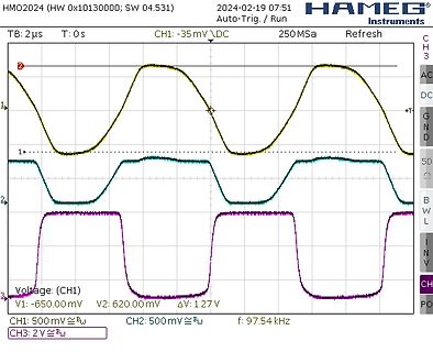
 Bild
Bild
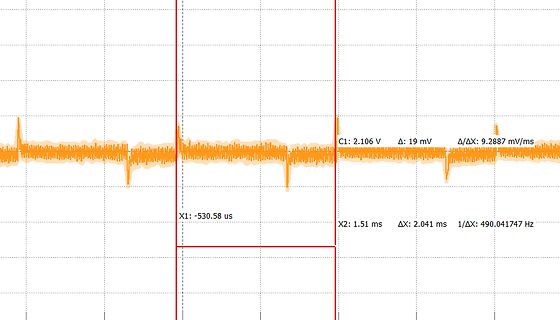
 Bild
Bild