-
Thread
Hilfe bei Schaltung PWM zu Analog
man sich sogar vorstellen, dass die Ausgabe ebenfalls über eine PWM erfolgt. Da reicht dann ein Low-Side-Transistor und ein Pullup mit nachgeschaltetem RC-Glied aus, weil die "krumme Kennlinie" dieser Treiberstufe ebenfalls in der Software korrigiert werden kann. Mike M. schrieb im Beitrag #7857647:
-
Thread
Motorsteuerung per H Brücke mit HIP4081
oder muss ich die Beschaltung irgendwie ändern? Wenn ich mich recht entsinne, verwenden die High-Side-Treiber Bootstrapkondensatoren. Um diese aufzuladen, müssen zuerst die zugeh. Low-Side-MOSFETs aktiviert werden. Die Ladungspumpe des Treibers ermöglicht dann auch Dauer-Ein der Highside-MOSFETs
-
Thread
Verständnisfrage FET
. Wenn die MOSFETs leiten, leiten sie (effizient) in beide Richtungen. Kann man auch beim High-Side schalten mit p-Channel-MOSFETs machen, oder auch high-side mit n-Channel-MOSFETs und Ladungspumpe. Die Body-Dioden kann man auch gewinnbringend einsetzen, indem man z.B. nur *einen* der MOSFETs einschaltet
-
 Bild
Bild
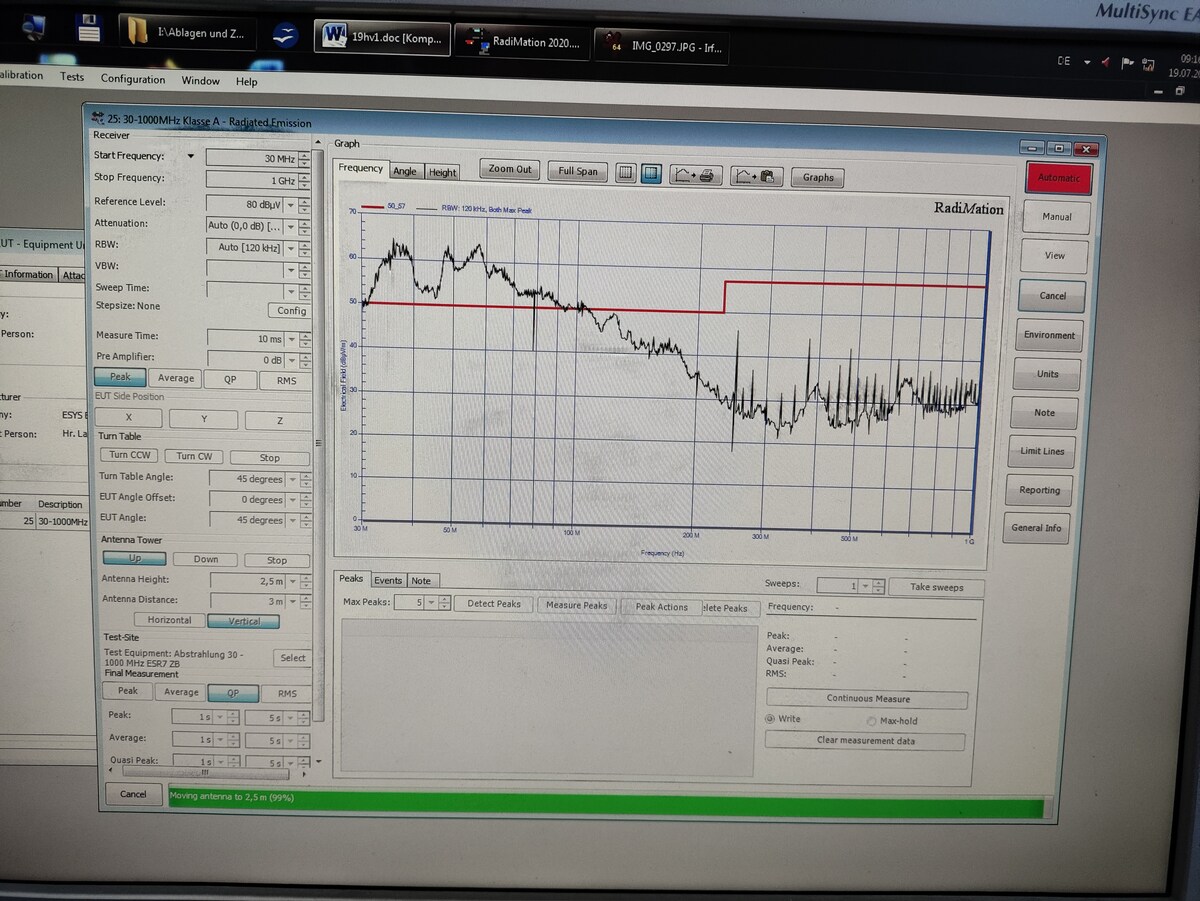
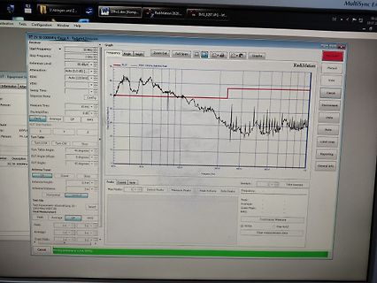
Foto eines Messbildschirms mit EMI-Spektrum
Attenuation: 0 dB RBW: 120 kHz VBW: 120 kHz Sweep Time: 10 ms Measure Time: 10 ms Peak Average QP RMS EUT Side Position Turn Table Angle: 45 degrees EUT Angle Offset: 0 degrees EUT Angle: 45 degrees Antenna Tower Antenna Height: 2,5 m Antenna Distance: 3 m Horizontal Vertical Peak Average QP RMS RadiMation 2020
-
Thread
Power Path Problem
) Versorgung über Schaltregler wegschalten, wenn das Gerät per USB versorgt wird (ActiveLow- High-Side Switch) b) Ideale Diode Max40200 oder sowas verwenden um die Rückwärtsbestromung zu verhindern c) Grundsätzlich denkbar wäre, die Versorgung des LAN-Parts im USB Fall zu unterlassen. Primär dient
nicht ideal). Der Max40200 ist relativ teuer mit 50-60Cent.. x2 sind es schon 1,20. Passende High-Side Switches gibts viele, auch günstig vom Chinesen zB CH217K (15Cent). Funktionieren denn meine angedachten Lösungen a und b überhaupt oder übersehe ich was? Gibts alternative Arten das zu lösen oder
-
 Bild
Bild
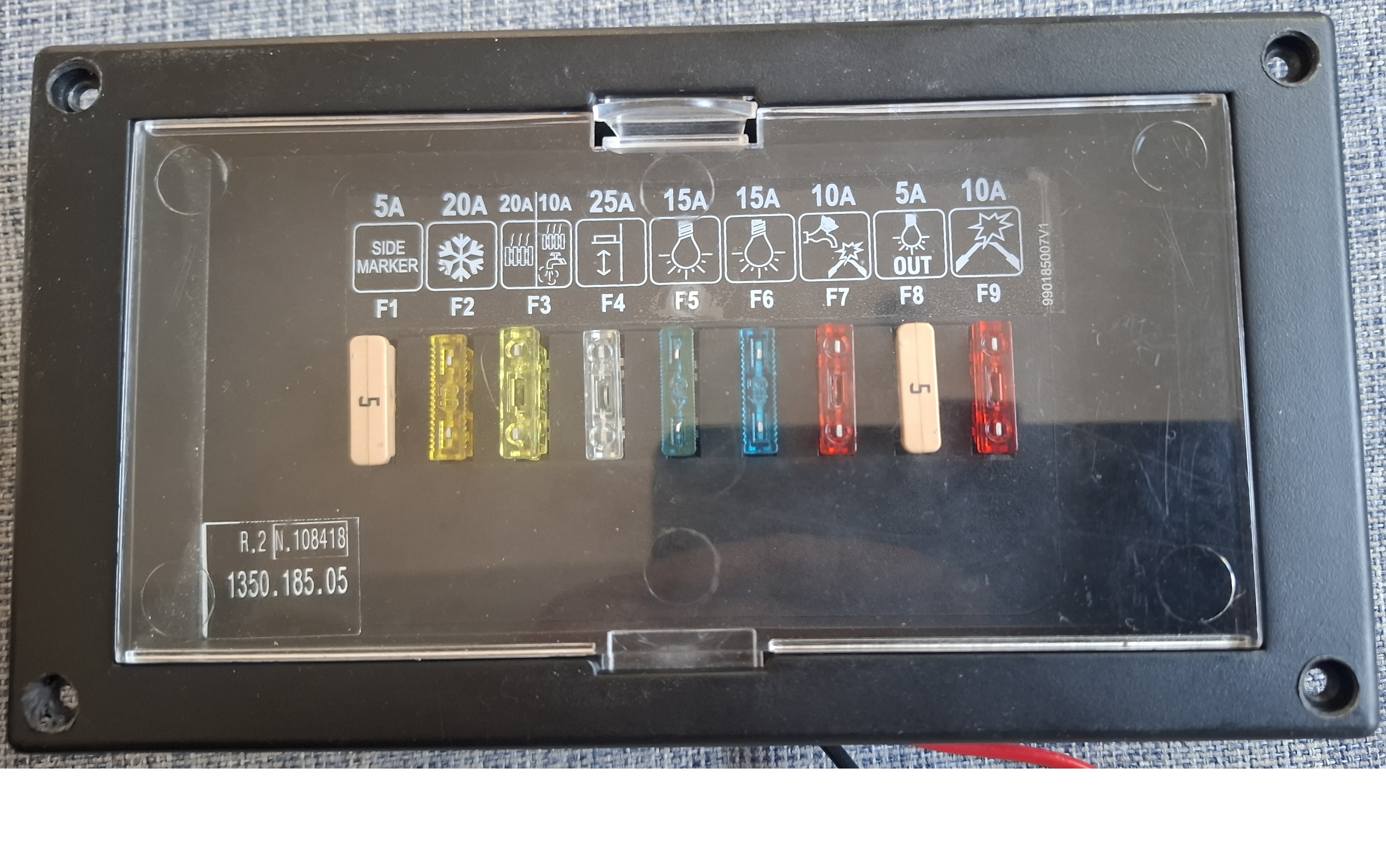
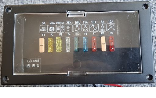
Sicherungshalter mit verschiedenen Sicherungen
5A SIDE MARKER F1 20A F2 20A F3 10A F4 25A F5 15A F6 15A F7 10A OUT F8 5A F9 10A 990185007V1 R.2 N.108418 1350.185.05
-
 Bild
Bild
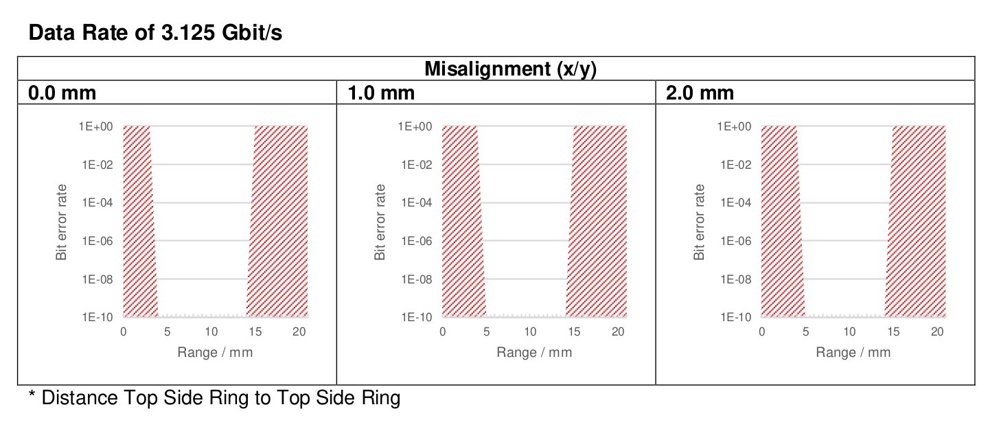
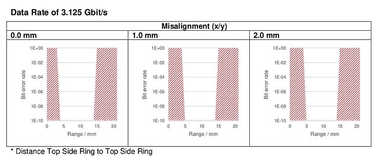
Diagramme der Bitfehlerrate bei verschiedenen Fehlstellungen
2.0 mm Bit error rate Range / mm 1E+00 1E-02 1E-04 1E-06 1E-08 1E-10 0 5 10 15 20 * Distance Top Side Ring to Top Side Ring
-
Thread
mit µC pin 5V schalten, suche "Ein-Bauteil-Lösung"
mit 2 Pins mehr zwecks Kühlung. Und mit allerlei Schnickschnack drin, was man sonst nur von High Side Switches kennt: https://www.infineon.com/cms/en/product/power/smart-power-switches/low-side-switches/classic-hitfet-12v/bts3800sl/
schrieb im Beitrag #7855234: > https://www.infineon.com/cms/en/product/power/smart-power-switches/low-side-switches/classic-hitfet-12v/bts3800sl/ Na super, ein proprietäres Footprint, damit man ja davon abhängig ist und nichts anderes bestücken kann. Ne, da bleibe ich lieber bei Wald und Wiesen MOSFETs
-
Thread
Blinking a mikrocontroller
kein "injected current" da er eben nicht über die Schutzdiode gegen VDD fließt sondern mit dem Low-Side Transistor gegen Masse geschaltet wird. Und damit gilt der Grenzwert von 25mA nicht.
-
 Bild
Bild
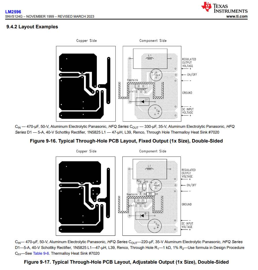
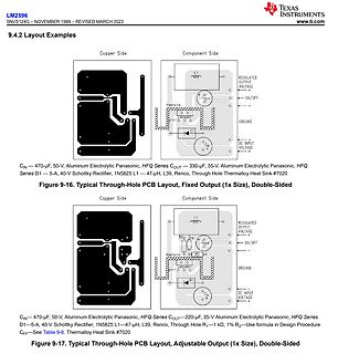
PCB Layout Beispiele für LM2596
SNVS124G – NOVEMBER 1999 – REVISED MARCH 2023 TEXAS INSTRUMENTS www.ti.com 9.4.2 Layout Examples Copper Side Component Side L1 REGULATED OUTPUT VOLTAGE ON/OFF Heatsink LM2596 OUT GROUND D1 DC INPUT VOLTAGE CIN COUT CIN — 470-µF, 50-V, Aluminum Electrolytic Panasonic, HFQ Series COUT — 330-µF, 35-V, Aluminum
-
Thread
LM2596S-3.3 gibt 3.9V raus..
Impendance Controlled PCB. Die Feedback-Line ist sehr kurz, auf eine Groundplane wurde auf der TOP Side verzichtet. Die 5V Seite macht exakt 4.99V... Ja ich weiß der Inductor ist mit 1.2A zu klein, aber es werden maximal 800mA gezogen. Natürlich habe ich mir die Ausgabe auf dem Oszi angesehen
-
Thread
Phillips TV Platine klackert dauerhaft
15x37GpUP5uO29tULaZ7Q4esWQY0PI6Q0/view?usp=drive_link > > Hat jemand eine Idee? > > Danke und Grüße! Und meine Side by Side Samsung hat ewig geklackert trtz das ich fast alle Elkos getauscht habe. Nur noch die letzte kleine scheiss 1μF kondesator war nicht erneuert und genau diese war der Grund! Deswegen zuerst
-
Artikel
Testseite
rechts mitte links unten rechts unten Name scope="col"|Score John 59 Jane 100 Bob 72 + style="caption-side:top;text-align:left;color:#FF0000"| Stückliste für die Steuerung Bauelement Bezeichnung JP1 Wannenstecker C1 Elko Stückliste. + verwendete Bauteile Name rowspan="2" | Wert rowspan="2" | Beschreibung
-
 Bild
Bild
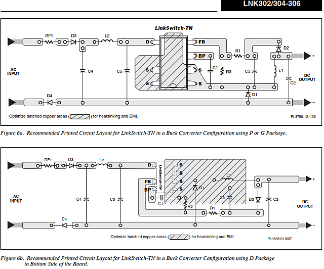
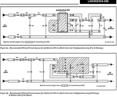
Schaltpläne für LinkSwitch-TN Buck Converter Layouts
Printed Circuit Layout for LinkSwitch-TN in a Buck Converter Configuration using D Package to Bottom Side of the Board.
-
Artikel
LED-Matrix
2,2V : Multiplexverhältnis (Spalten): 1:5 : Zeilen in der Matrix: 8 : Sättigungsspannung des Low Side Transistors, hier Q9-Q13 mit ca. 0,7V : Basis-Emitter-Spannung des High Side Transistors, hier Q1-Q8 ca. 0,7V Gesucht: : Dauerstrom der Zeilentreiber = Pulsstrom der LEDs : Pulsstrom der Spaltentreiber
LED-Stränge: 7V : Multiplexverhältnis (Zeilen): 1:4 : Spalten in der Matrix 8 : Sättigungsspannung des Low Side Switch, hier IC1 mit ca. 1V : Sättigungsspannung des High Side Switch, hier IC2 mit ca. 2V Gesucht: : Dauerstrom der Spaltentreiber = Pulsstrom der LEDs : Pulsstrom der Zeilentreiber : Vorwiderstand
-
Thread
Stromverbrauch 74 Logic ICs
@ 150GradC) PBHV8115T (120V SOT23 100nA @ 25 GradC, 10uA @ 125 GradC, NXP BISS) TPS22860 (5V high side power switch 2nA) hochsperrende MOSFETs: Ohne Bulkdiode. ALD1107 (400pA max., 4nA bei 125 GradC) SD5000 BSS83 (10nA max.) vs. BS170 (500nA) BSS295 (1uA max., 50uA bei 125 GradC) wer besser als Datenblatt
-
 Bild
Bild
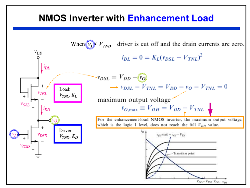
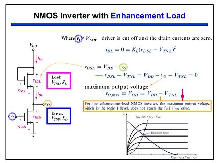
NMOS Inverter mit Enhancement Load Schaltplan und Kennlinie
NMOS Inverter with Enhancement Load When vI < VTND driver is cut off and the drain currents are zero. iDL = 0 = KL(vDSL - VTNL)^2 vDSL = VDD - vO vDSL - VTNL = VDD - vO - VTNL = 0 maximum output voltage vO,max = VOH = VDD - VTNL For the enhancement-load NMOS inverter, the maximum output voltage, which is the logic 1 level, does not reach the full VDD value. Load: VTNL, KL Driver: VTND, KD iD vDS (sat) = vGS - VTN Transition point vDD - VTNL vDD vDS
-
 Bild
Bild
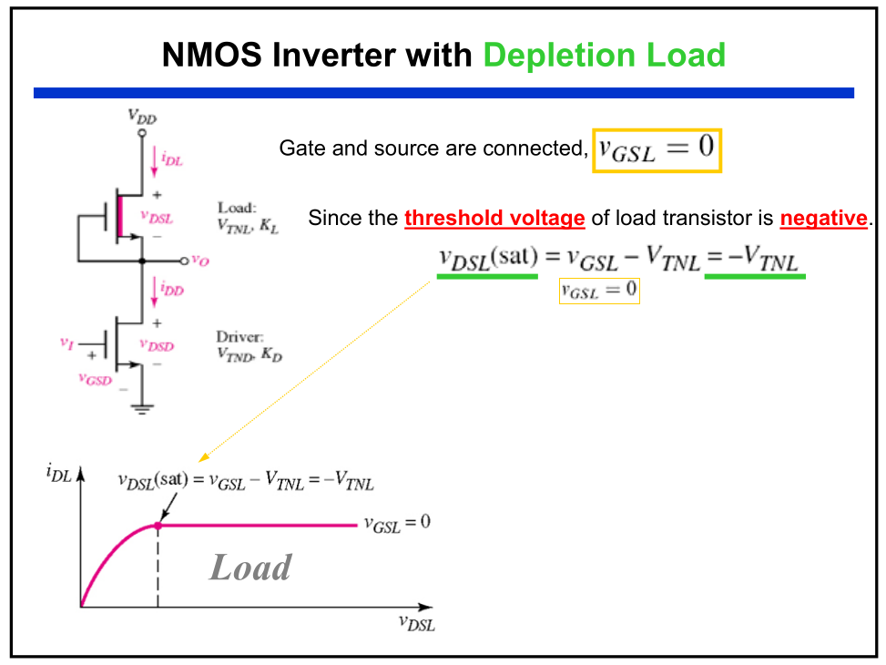
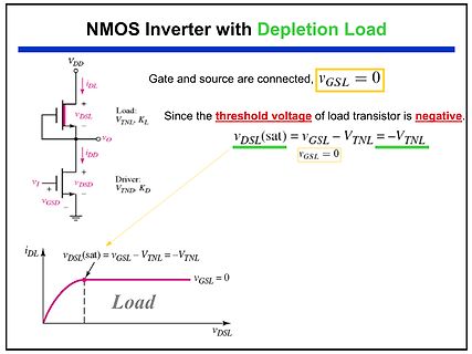
NMOS Inverter mit Depletion Load Erklärung
NMOS Inverter with Depletion Load VDD iDL + vDSL Load: VTNL, KL Gate and source are connected, vGSL = 0 Since the threshold voltage of load transistor is negative. vDSL(sat) = vGSL - VTNL = -VTNL vGSL = 0 vi + vDSD Driver: VTND, KD - VDD iDL vDSL(sat) = vGSL - VTNL = -VTNL vGSL = 0 Load vDSL
-
Thread
INA219 Eigang potentialfrei
R. schrieb im Beitrag #7848903: > Das IC kann nicht, was du willst. Passt, für nur Strom low-side ist er unpassend. > Es wird zerstört werden. Darüber kann man streiten.
-
Thread
Unterschied der verrichteten Arbeit zwischen 2 Magnete
Trump administration will treat climate change for what it is, a global physical phenomenon that is a side effect of building the modern world." ➝ “I wanted to play a role in reversing what I believe has been a very poor direction in energy policy. The previous administration’s policy was focused myopically
-
Thread
Geeigneter Mikrocontroller für Zellmessungen
interessant, Danke! Dem kann ich evtl. sogar NaIon beibringen. Was sind denn die Vorteile vom High Side Schalten?
-
 Bild
Bild
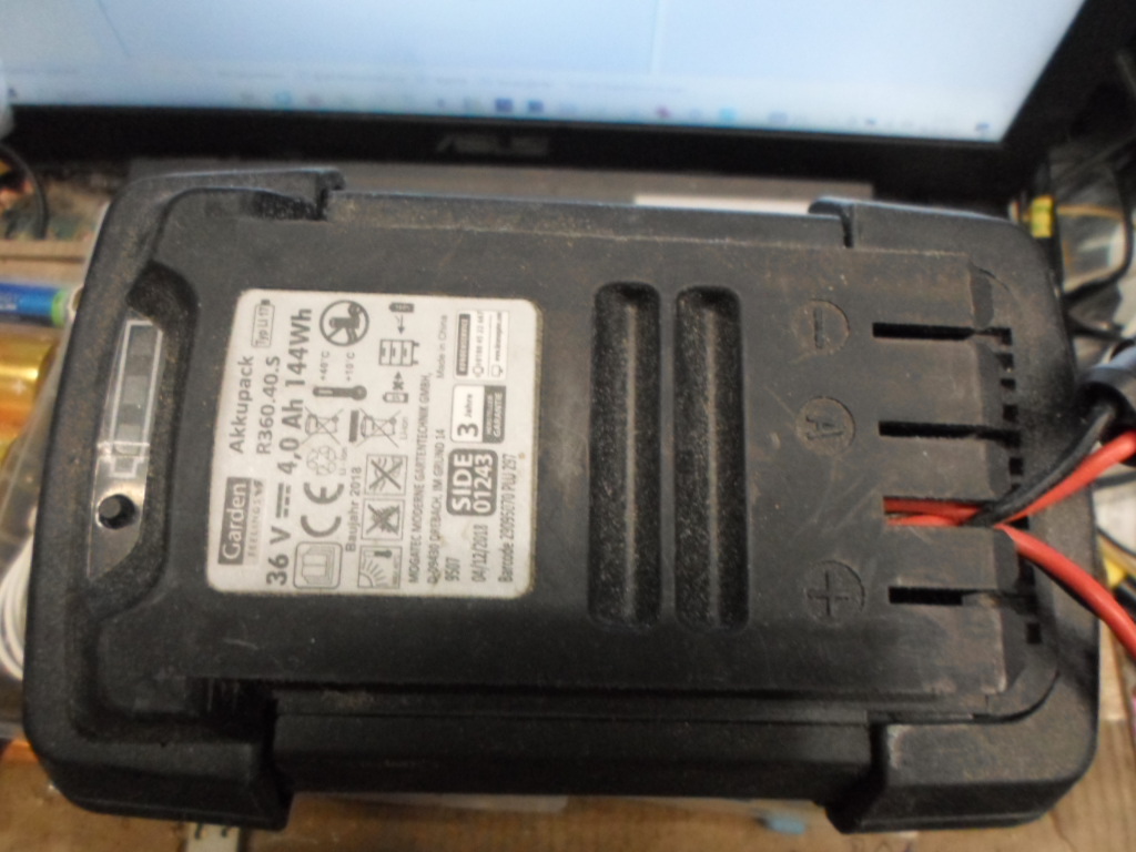
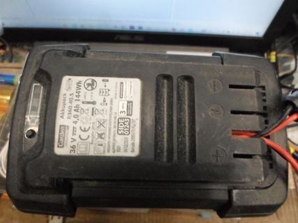
Akkupack für Gartengeräte
Garden R360.40.S 36 V 4,0 Ah 144Wh Baujahr 2018 Made in China SIDE 3 04/12/2018 01243 Barmode 29959270 PLU 297
-
Thread
Ubuntu pyvisa: Verbindung zum USB-seriellen Gerät
/usr/bin/env python3 # test USB SCPI Commands with an Arduino as Instrument # # Arduino test side: # https://github.com/Vrekrer/Vrekrer_scpi_parser/blob/master/examples/SCPI_Dimmer/SCPI_Dimmer.ino # # 250317 mchris import pyvisa import time # Define the serial resource address (update
-
 Bild
Bild
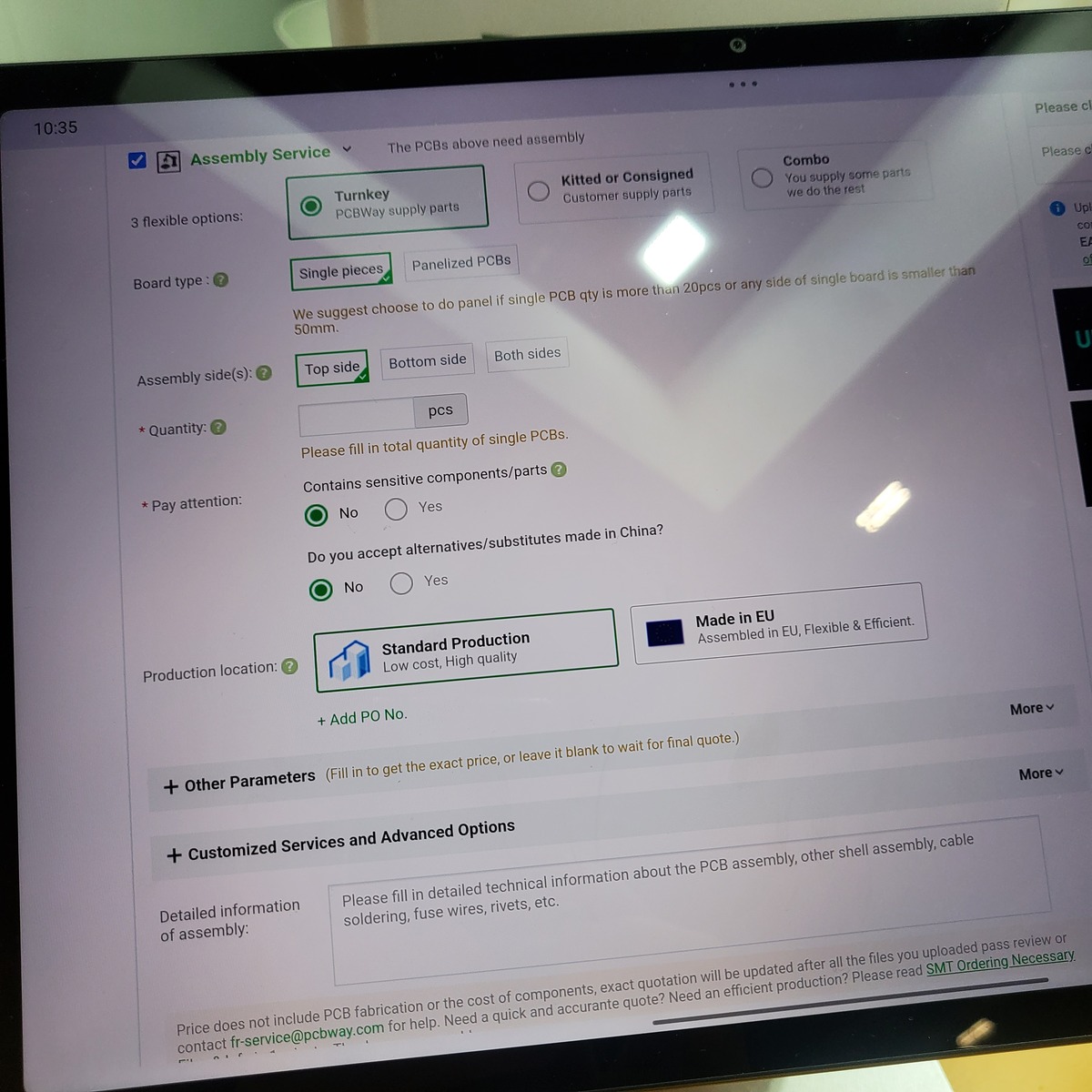
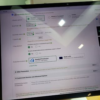
Abfotografierter Bildschirm einer PCB-Assembly-Webseite
Single pieces Panelized PCBs We suggest choose to panel if single PCB qty is more than 20pcs or any side of single board is smaller than 50mm. Assembly side(s): Top side Bottom side Both sides Quantity: pcs Please fill in total quantity of single PCBs. Contains sensitive components/parts: No Yes Do you
-
Thread
Zusätzlicher 2-pin Lüfter an 4-pin Anschluss
es wert. Im Zweifel kann man natürlich auch nochmal ein Mosfet damit schalten und dann sogar High-Side arbeiten. Allerdings ist anzunehmen dass normale 2 Pin Lüfter auf PWM an ihrer Versorgung anders reagieren als 4 Pin Lüfter mit extra PWM Eingang und das Ergebnis nicht zufriedenstellend sein wird
-
Thread
[V] 77x VND5T100AJTR-E Double Ch High Side 58V 100mOhm 22A
Verkaufe 77 Stück STMicroelectronics VND5T100AJTR-E 2-Kanal High-side Treiber 58V 100mOhm 22A Verpackung wurde geöffnet, die ICs waren aber immer in einer ESD Verpackung und natürlich einer ESD geschützten Umgebung. Preis für alle zusammen 77€ plus Versand aus Österreich
schrieb im Beitrag #7841950: > Verkaufe 77 Stück STMicroelectronics VND5T100AJTR-E 2-Kanal > High-side Treiber 58V 100mOhm 22A Falls sich jemand für das Datenblatt interessiert..:-) https://www.st.com/resource/en/datasheet/vnd5t100aj-e.pdf Interessantes Bauteil..
-
 Bild
Bild
Werbebanner für RISC-V und DeepSeek-Unterstützung
Supports local deployment of Deepseek-R1 distillation models, which helps users realize efficient end-side intelligence and ensure the security and controllability of data processing through offline deployment at the edge. Leading arithmetic energy efficiency With the streamlined RISC-V architecture and

-
 Bild
Bild
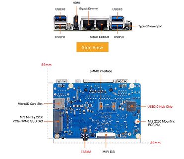
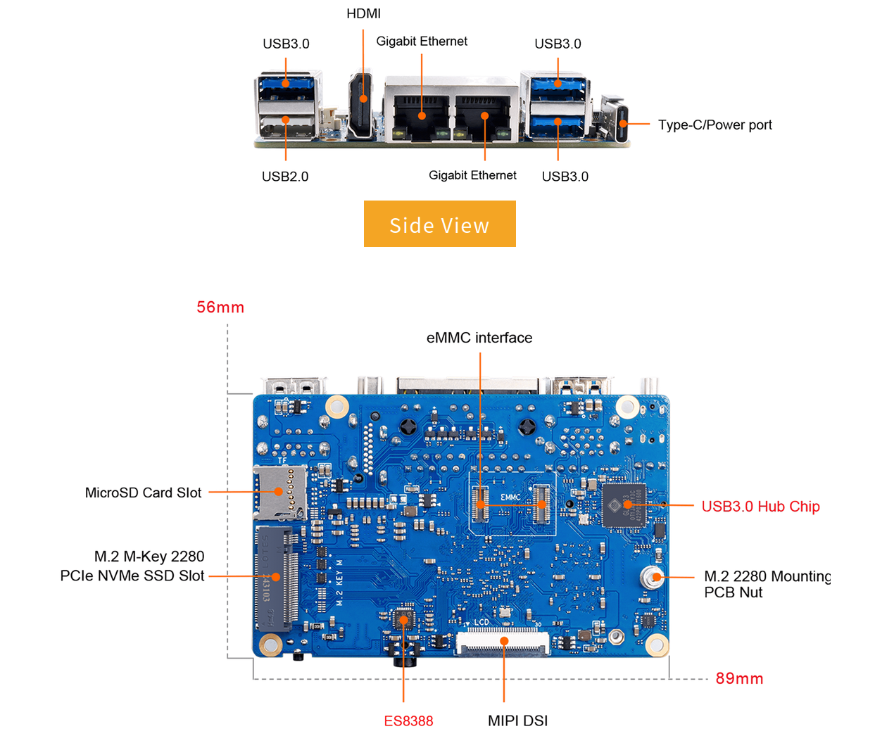
Beschriftete Ansichten einer Single Board Computer Leiterplatte
HDMI USB3.0 Gigabit Ethernet USB3.0 Type-C/Power port USB2.0 Gigabit Ethernet USB3.0 Side View 56mm eMMC interface MicroSD Card Slot M.2 M-Key 2280 PCIe NVMe SSD Slot USB3.0 Hub Chip M.2 2280 Mounting PCB Nut ES8388 MIPI DSI 89mm