-
Thread
GD32F303: Bootloader der Originalfirmware für Open Source Projekt nutzen
Erkenntnisse, aber leider keine Lösung. Mit dem originalen Bootloader hat PB4 kontinuierlich 3.3V, also high gesetzt. PB8 schickt alle 250ms einen 5ms langen High Puls. Wenn ich das in meiner Firmware nachbaue, zieht aber offensichtlich irgendwas die Signale von PB4 und PB8 auf ca. 0,3V runter, so daß
Nein, war nur tricky, dass der Pin auf low gezogen werden muss. Auf high gesetzt hatte ich alle Pins durchprobiert. Habe PC2 jetzt auf Open Drain konfiguriert, da er 4,3V auf GND ziehen muss.
-
Thread
4Pin luefter Spezifikation
entnehmen kannst so gab es zumindest mal Luefter die dies nicht durch direkte Verhaeltnismaessung der Low/High Zeiten gemacht haben. Vanye
-
Thread
ESP32-H2 will nicht schlafen
// disable ALL wakeup sources (just for safety) gpio_wakeup_enable(BUTTON_GPIO, GPIO_INTR_HIGH_LEVEL); // LOW -> HIGH wakeup esp_sleep_enable_gpio_wakeup(); // USB-CDC vor Sleep deaktivieren usb_serial_jtag_driver_uninstall(); sleep_indicator_sleeping(); // set GPIO4 to HIGH // SLEEP esp_light_sleep_start(); sleep_indicator_awake(); // set GPIO4 to LOW // USB-CDC nach Sleep neu starten reinit_usb_cdc(); ESP_LOGI(TAG, "Uuaaa, i woke
-
Thread
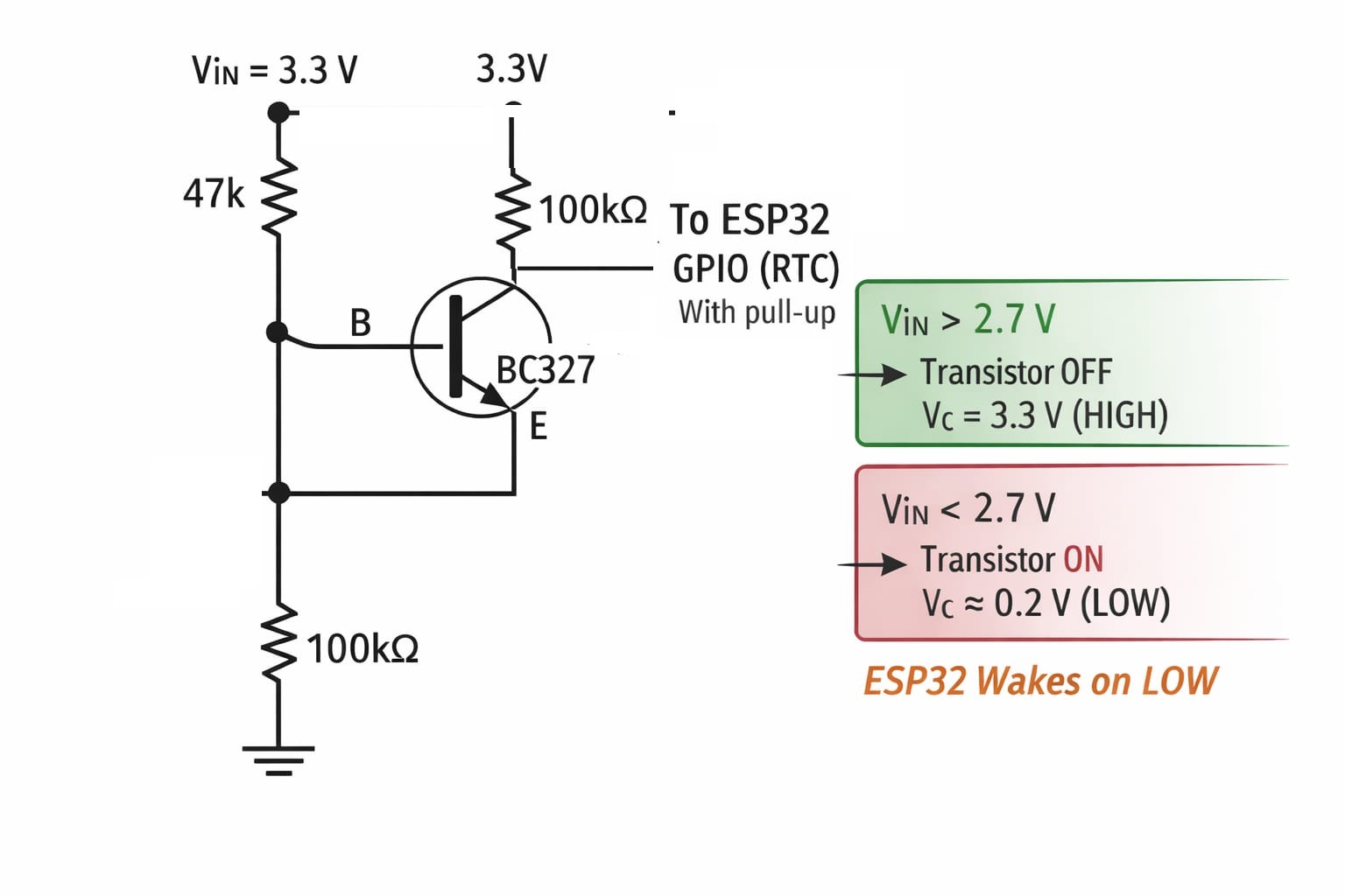
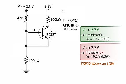
ESP32 Wake-up bei Unterspannung (~2,7 V) mit BC327 – funktioniert diese Schaltung?
Pull-up vom GPIO nach 3,3 V Gedanke dahinter: Bei VIN > ~2,7 V ist der Transistor aus → GPIO = HIGH Bei VIN < ~2,6–2,7 V wird V_BE leitend → Transistor zieht den GPIO auf LOW → ESP32 wacht auf Mir ist bewusst: Die Schaltschwelle ist nur näherungsweise durch V_BE definiert Temperatur- und
analoge Bauteile. Sie schalten nicht plötzlich an/aus wie Relais. Fer EDP bekommt also nicht nur HIGH und LOW Signale, sondern auche alle unzulässigen Spannungen dazwischen. Dabei erhöht sich seine Stromaufnahme und wie er digital darauf reagiert ist ungewiss. Du brauchst eine Referenzquelle und
-
 Bild
Bild
Schaltplan einer Transistor-Schaltung zur ESP32-Wecksteuerung
3.3 V 47k 3.3V 100k To ESP32 GPIO (RTC) With pull-up BC327 VIN > 2.7 V Transistor OFF Vc = 3.3 V (HIGH) VIN < 2.7 V Transistor ON Vc ≈ 0.2 V (LOW) ESP32 Wakes on LOW 100kΩ
-
 Bild
Bild
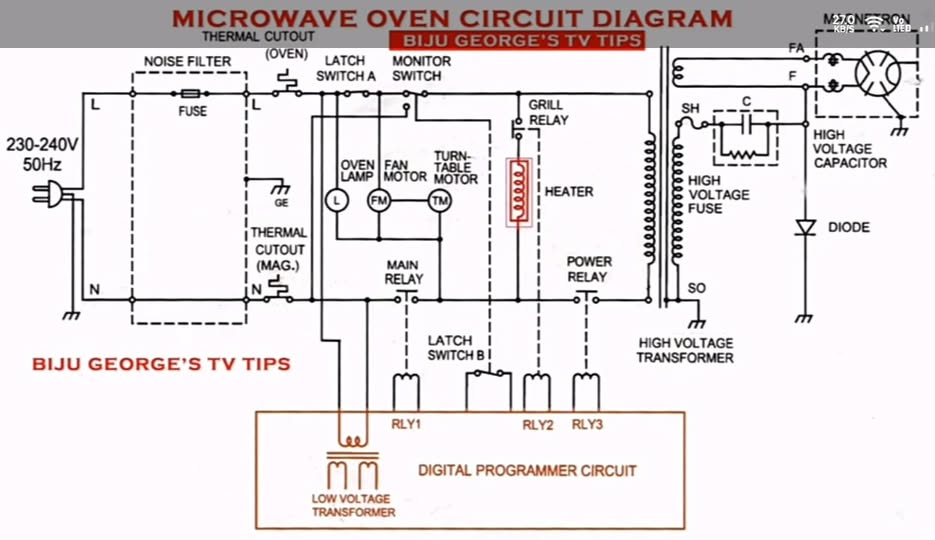
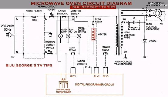
Schaltplan eines Mikrowellenherds
OVEN LAMP FAN MOTOR TABLE MOTOR MAIN RELAY LATCH SWITCH B RIY1 RLY2 RLY3 DIGITAL PROGRAMMER CIRCUIT LOW VOLTAGE TRANSFORMER GRILL RELAY HEATER POWER RELAY HIGH VOLTAGE FUSE HIGH VOLTAGE TRANSFORMER HIGH VOLTAGE CAPACITOR DIODE SO F
-
 Bild
Bild
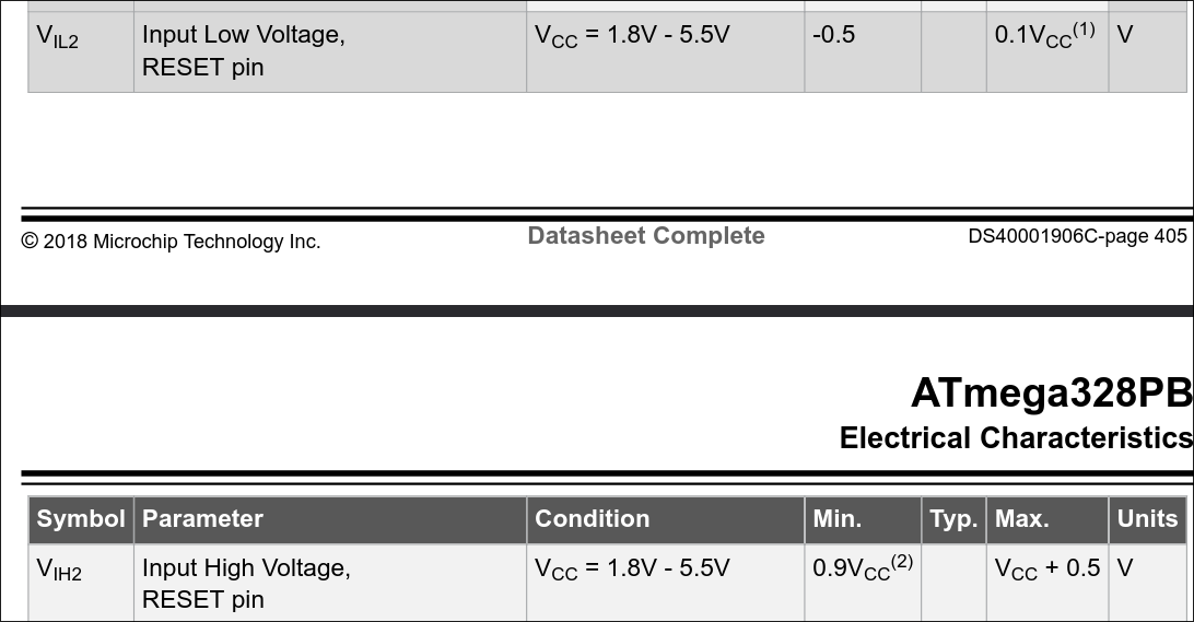
Ausschnitt aus einem Datenblatt des ATmega328PB
VIL2 Input Low Voltage, RESET pin VCC = 1.8V - 5.5V -0.5 0.1VCC(1) V © 2018 Microchip Technology Inc. Datasheet Complete DS40001906C-page 405 ATmega328PB Electrical Characteristics Symbol Parameter Condition Min. Typ. Max. Units VIH2 Input High Voltage, VCC = 1.8V - 5.5V 0.9VCC(2) VCC + 0.5 V

-
Thread
Atmega 328PB lässt sich nicht programmieren
reset, Hellblau ist MOSI und Lila ist MISO. Das triggerniveau habe ich für das Bild auf das Reset-High(Low?) Niveau gesetzt, dass man da die 1.0V erkennt. Christian schrieb im Beitrag #7984510: > Die Diode am Regler würde ich entfernen(überbrücken) und die Schaltung > generell nicht über den Prog-Stecker
weit genug runterzukommen. Wenn ich das richtig verstehe (Screenshot angehängt) muss das Signal bei High(Low?) zwischen -0.5 und 1V liegen. Da ist 1V ziemlich grenzwertig... Wie muss ich das mit dem Kabelbruch verstehen? Warum würde ein Kabelbruch verhindern, dass das Signal auf 0V herunterkommt? Wenn
-
Thread
Widerbelebung Oldtimerradio aus 1973
bei gedrücktem "M" die Bluetoothmusik dudelt. Ich hoffe, dass dann in Verbindung mit einem guten high-low-adapter und einer kleinen Endstufe ordentliche Musik im Oldi herrscht.
gedrücktem "M" > die Bluetoothmusik dudelt. Ich hoffe, dass dann in Verbindung mit einem > guten high-low-adapter und einer kleinen Endstufe ordentliche Musik im > Oldi herrscht. Alternative Lösung: https://www.computerbase.de/news/mobilitaet/frankfurt-stereo-blaupunkt-bringt-70er-jahre-radio-mit-moderner-technik
-
 Bild
Bild
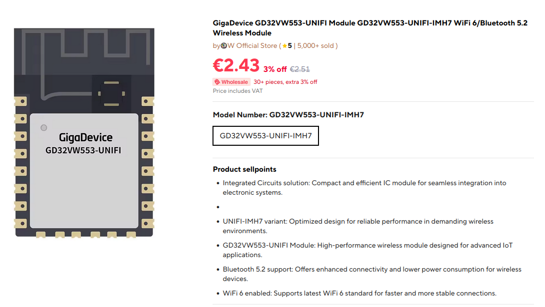
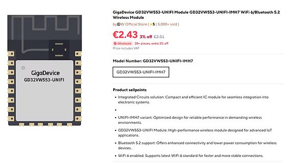
GigaDevice GD32VW553-UNIFI WiFi/Bluetooth Modul Produktseite
Optimized design for reliable performance in demanding wireless environments. • GD32VW553-UNIFI Module: High-performance wireless module designed for advanced IoT applications. • Bluetooth 5.2 support: Offers enhanced connectivity and lower power consumption for wireless devices. • WiFi 6 enabled: Supports
-
Thread
ESP32 und 240Stück WS2812B
V6 bestellen. Die Beschaltung des Pegelwandlers passt auch? Manche sagen, unbenutze Eingänge auf High, andere sagen auf Low legen.
bestellen. Die Beschaltung des > Pegelwandlers passt auch? Manche sagen, unbenutze Eingänge auf High, > andere sagen auf Low legen. Wenn ich das Datenblatt richtig deute brauchst du bei den V6 keinen Pegelwandler, High-level input voltage VIH 0.55VDD, also ca. 2,8V bei 5V Versorgung der LEDs.
-
 Bild
Bild
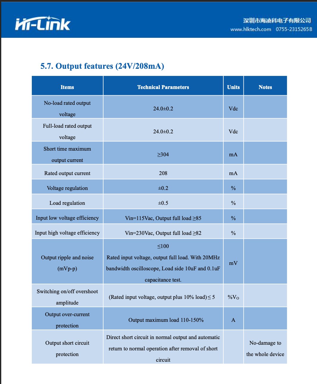
Tabelle der Ausgangsmerkmale eines Netzteils
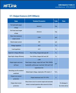
current ≥304 mA Rated output current 208 mA Voltage regulation ±0.2 % Load regulation ±0.5 % Input low voltage efficiency Vin=115Vac, Output full load ≥85 % Input high voltage efficiency Vin=230Vac, Output full load ≥82 ≤100 % Output ripple and noise (mVp-p) Rated input voltage, output full load. With
-
Thread
Mosfet Modul mit PWM ansteuern MKS GEN_L V2.1
NSPW500BS). D3 dient als optische Anzeige des Eingangssignals. M2 (BSP89) ist ein N-MOSFET, der als Low-Side-Schalter arbeitet: Gate wird direkt vom Pulssignal angesteuert. Bei High-Pegel schaltet M2 durch und zieht den Knoten nach Masse. Dadurch entsteht ein sauberes, lastfähiges Logiksignal
. B. Heizung, Lampe, Widerstand). V2 (36 V) ist die Versorgung der Last. Ablauf: Treiber HIGH → Gate von M1 wird hochgezogen → MOSFET leitet → Laststrom fließt Treiber LOW → Gate entladen → MOSFET sperrt → Last stromlos Zweck: Schalten einer niederohmigen, leistungsstarken Last mit hoher
-
 Bild
Bild
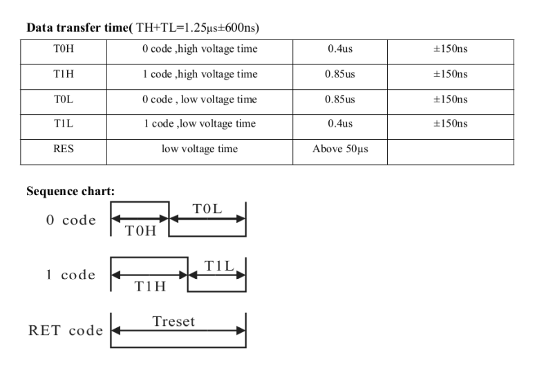
Tabelle und Diagramm der Datentransferzeiten
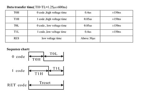
Data transfer time(TH+TL=1.25µs±600ns) T0H 0 code,high voltage time 0.4us ±150ns T1H 1 code,high voltage time 0.85us ±150ns T0L 0 code, low voltage time 0.85us ±150ns T1L 1 code,low voltage time 0.4us ±150ns RES low voltage time Above 50µs Sequence chart
-
Thread
Handbetriebenen Drehgeber ohne Timer auswerten
rp2040-mh-2.png: Wie zuvor, aber mit anderer Zeitbasis. Die Hysterese sorgt für einen sauberen Low-High- und High-Low-Übergang. rp2040-oh-1.png: Die Hysterese wurde softwaremäßig deaktiviert, die Schaltschwellen für das ansteigende und das abfallende Signal sind gleich -> keine Hysterese.
box) außer Tritt > bringen können. Wenn währenddessen der zweite Kanal einen konstanten Pegel (high oder low) liefert, sollte dies kein Problem sein. > Um eine volle Periode des Gebers zu erfassen, bräuchte man einen > (motorischen) Antrieb mit gleichbleibender Drehzahl. Zeichne ich 10 s > auf
-
Thread
MicroPython 1.27, Qt for Microcontrollers und andere Softwareupdates
provided for all three of these configurations, as well as for the new ESP32-C5. Support for the low-power and high performing STM32U5xx series is also added in this release, supporting USB, ADC, DAC, UART, I2C, SPI and RTC, with a board profile for the NUCLEO-U5A5ZJ-Q. [/c] Neuerung Nummero
foreign processors. • DHRUV64 supports prototype development for new system architectures at lower cost. • India already has 20% of the world’s chip design engineers. DHRUV64 further helps in building a strong pipeline of skilled semiconductor chip professionals. • The success of DHRUV64
-
 Bild
Bild
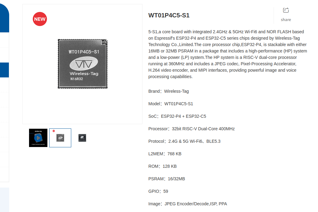
Produktseite des WT01P4C5-S1 Mikrocontrollers
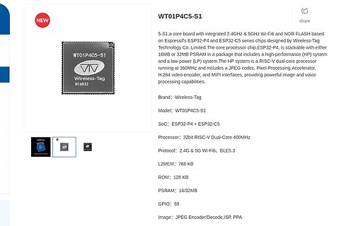
processor chip,ESP32-P4, is stackable with either 16MB or 32MB PSRAM in a package that includes a high-performance (HP) system and a low-power (LP) system.The HP system is a RISC-V dual-core processor running at 360MHz and includes a JPEG codec,Pixel-Processing Accelerator, H.264 video encoder, and MIPI
-
 Bild
Bild
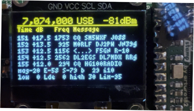
Display eines SDR-Empfängers mit Messwerten
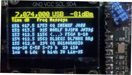
..> F5GN R-10 154 +12.5 2562 DL2EGS DL7MDX RRG 155 +12.0 234 CQ HG100RADIO Hag-20 E-52 S-79 dB i10 low 0 Lde 0 high 30 Lin-95
-
 Bild
Bild
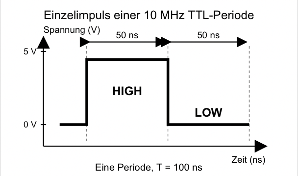
Diagramm eines 10 MHz TTL-Impulses
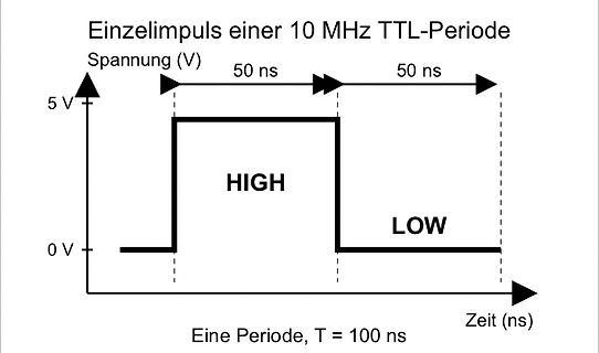
Einzelimpuls einer 10 MHz TTL-Periode Spannung (V) 5 V 50 ns 50 ns HIGH LOW 0 V Zeit (ns) Eine Periode, T = 100 ns
-
Thread
EMS Fertigung: 95% Ausfallquote
circuitry requires an input clock frequency between 50kHz and 200kHz to get maximum resolution. If a lower resolution than 10 bits is needed, the input clock frequency to the ADC can be higher than 200kHz to get a higher sample rate.“ Und in den Maximum ratings wird ein Genauigkeitswert für 1Mhz ADC-Frequenz
-
Thread
Mehr Zusammenarbeit zwischen CIX und OrangePi, Raspberry Pi-Sicherheitsupdate uvam
interested in improving the software for the CIX P1. It’s unclear whether any of that will help fix the high idle power consumption, which is a non-starter for some people. I suspect I might require SoC-level power management optimizations that would probably have to be handled by CIX themselves, although
folgendes: [c] With support for both 2.4 and 5 GHz bands, both MCUs deliver superior throughput, low latency, and reduced power consumption. The dual-band capability dynamically selects the most suitable band based on real-time conditions, ensuring a stable and high-speed connection even in environments
-
Thread
DS3231 im VBAT Betrieb kein SQW Interrupt möglich?
dem DS Board ein Pullup drauf ist (was recht wahrscheinlich ist) und ich den VCC mit dem GPIO auf LOW ziehe anstelle ihn "offen" zu lassen dann wird der Pullup zum Pulldown und den Open-Drain Output des DS stören?
Ich hoffe, du ziehst auch die I2C Leitungen auf LOW, wenn du der RTC ihre Versorgungsspannung weg nimmst. Sonst hast du auch dort verbotene Pegel. Warum machst du das überhaupt?
-
 Bild
Bild
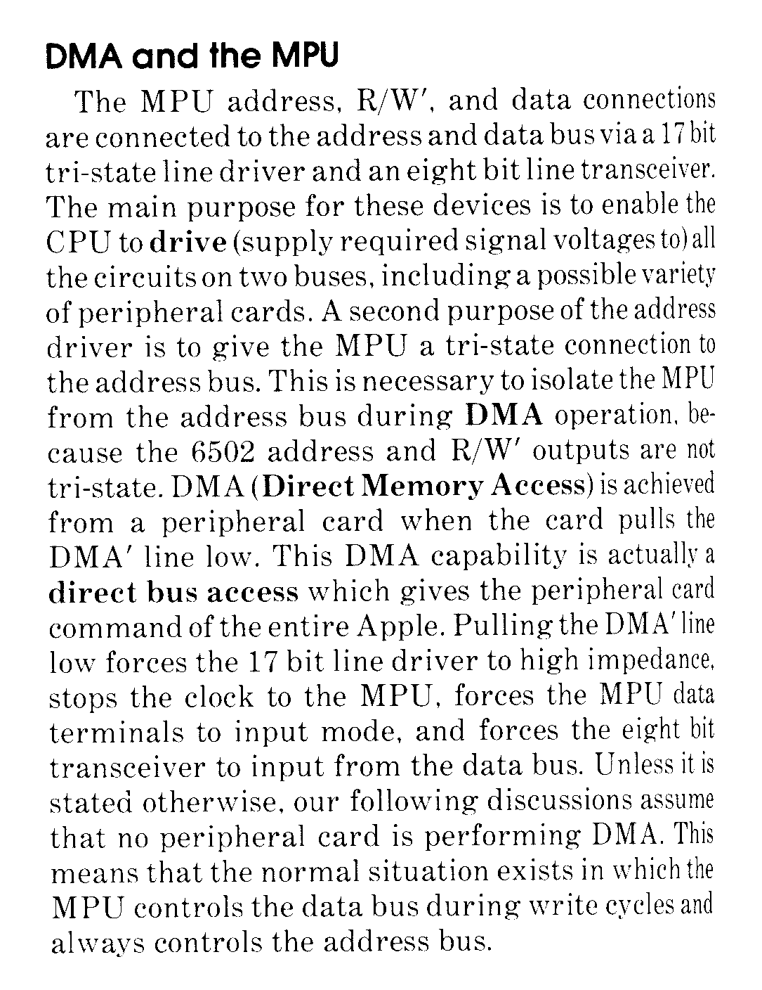
Text über DMA und MPU Funktionsweise
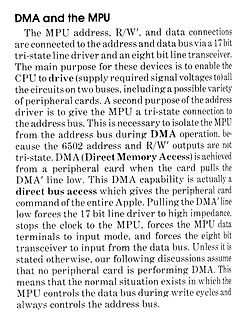
tri-state. DMA (Direct Memory Access) is achieved from a peripheral card when the card pulls the DMA' line low. This DMA capability is actually a direct bus access which gives the peripheral card command of the entire Apple. Pulling the DMA' line low forces the 17 bit line driver to high impedance, stops the
-
 Bild
Bild
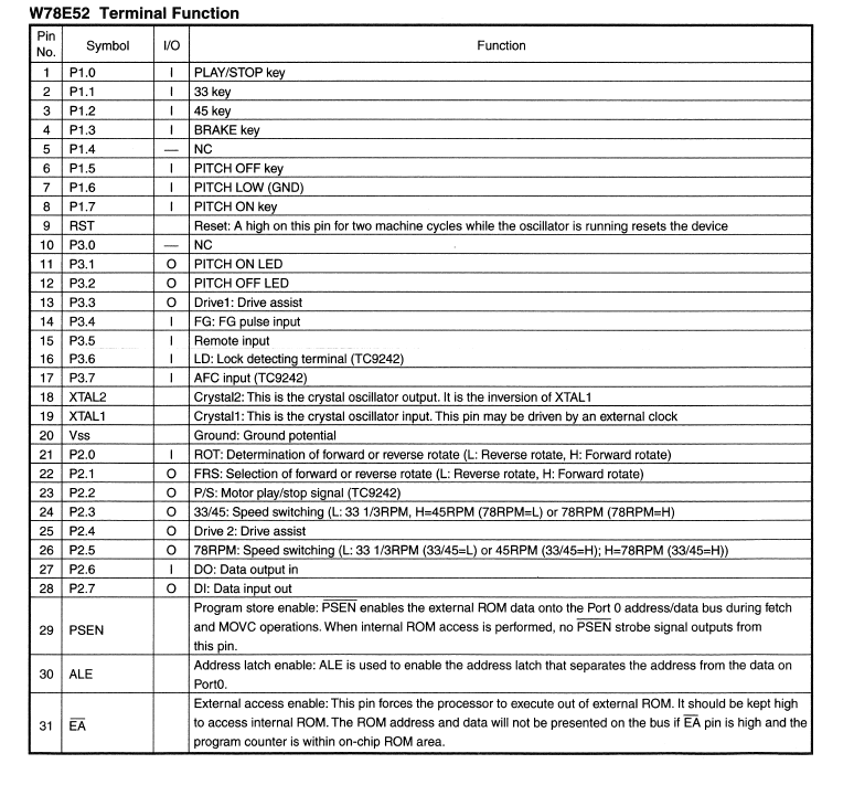
Tabelle der Pin-Belegungen für W78E52
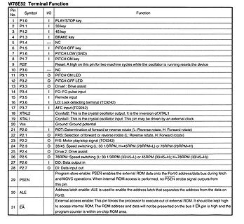
P1.1 I 33 key 3 P1.2 I 45 key 4 P1.3 I BRAKE key 5 P1.4 I NC 6 P1.5 I PITCH OFF key 7 P1.6 I PITCH LOW (GND) 8 P1.7 I PITCH ON key 9 RST Reset: A high on this pin for two machine cycles... 10 P3.0 NC 11 P3.1 O PITCH ON LED 12 P3.2 O PITCH OFF LED 13 P3.3 O Drive1: Drive assist 14 P3.4 I FG: FG pulse
-
Thread
TWI - Pull-Up ungewöhlich klein
Wenn der Master Clock Stretching unterstützt, dann kann der Slave die Clock-Leitung länger auf LOW, wenn er mehr Zeit braucht. Der Master kann nicht unterscheiden, ob spätere HIGH-Pegel von Clock Stretching oder einer langsam steigenden Flanke durch einen zu schwachen Pullup stammt. In Grenzen
-
Thread
Softwareupdates, Mikrocontroller und Neues von Arduino und Raspberry Pi
stehen die vier folgenden neuen Funktionen zur Verfügung: [c] • Modulino Latch Relay – Switch high-power loads with a simple signal • Modulino Light – Detect ambient brightness and react to changes in lighting • Modulino Joystick – Add intuitive interactive control to your gaming or robotics
nRF54L Series. . . . Uniquely, the nRF54LV10A is also the world’s first Bluetooth LE SoC to combine low voltage with Bluetooth Channel Sounding support. – via https://www.nordicsemi.com/Nordic-news/2025/12/Nordic-unveils-nRF54LV10A-a-breakthrough-low-voltage-Bluetooth-LE-SoC [/c] Ebenda findet sich
-
Thread
Hilfe bei CMOS Testschaltung
Maximilian schrieb im Beitrag #7977705: > liegt Low am Und-Gatter U2D > an und dieses gibt High zum CLR Eingang des CD4060. Das 4011 ist ein NAND. Der Ausgang wird low (Schaltung rennt los) wenn beide Eingänge high sind. Ist also der Test Taster
Ausgänge von den beiden CD4514 Naja, nicht ganz. Wenn der obere 4514 das tut, was er soll, müsste Q0 high werden. Nur /E auf high stellt alles auf low.
-
Thread
Suche Transistor C3333
Suche nach C3333 https://www.alldatasheet.com/datasheet-pdf/pdf/30185/TOSHIBA/C3333.html npn High Voltage Switching Applications Color TV Chroma Output Applications High voltage: VCEO = 250 V Low Cre: 1.8 pF (max) Complementary to 2SA1320 https://www.reichelt.de/de/de/shop/produkt/bipolartransistor_npn
-
Thread
Isolation eines Servo-PWM-Signals per Optokoppler
Hast du übersehen, das der 6N137 negierten Ausgang hat? In Ruhe ist der Ausgang high und bei aktiver LED ist er low. Je nach Beschaltung ist das auch bei 'normalen' Optokopplern der Fall.
die Frequenz in weiten Grenzen egal. Steuergröße für klassische Modellbauservos ist die Dauer des High-Pulses. Jens M. schrieb im Beitrag #7977990: > Finn schrieb: >> beeinflusst die Erdung des Osziloskops meine >> Messung? > > Normal nicht. Fehlendes Bezugspotential aber schon. Das kommt
-
Thread
Eprom von Denon DJ Laufwerk defekt Winbond 78e52
33 auf 45 umschalten möchte muss ich doch an Pin 3 das Signal abfragen, wenn dieses Signal auf high schaltet durch tastendruck setzt die mcu pin 36 auf low, pin 37 auf high und pin 24 auf high. Motor start Taste pin 1 geht auf high, Software setzt Pin 23 auf high. Motor sollte anlaufen. Was ich
und schauen was geht /nicht geht Vorsicht! Du solltest prüfen ob die Steuerbits wirklich alle high-active sind, also die Funktion aktiv ist, wenn das Portbit eine '1' ausgibt bzw. wenn eine '1' am Portbit anliegt. In der Hardware werden Schalter und LEDs gerne auf Masse geschaltet und sind dann low-active
-
Thread
Back-to-Back PMOS & Diodenplatzierung
Anforderungen und wie Du diese Anforderungen ermittelt hast. Wie kommst Du auf die 30V? Warum schaltest Du High-Side und nicht Low-Side? "30V mit 1-2A" ist nicht die eigentliche Anwendung. Sondern z.B. "ich möchte mein Terrarium mit einer Heizfolie heizen. Solltemperatur ist xxx, Außentemperatur ist yyy, Heizfolie
davon. Du darfst davon ausgehen, dass ich die Anforderungen korrekt ermittelt habe. Und stimmt, "high-seitige Schaltung" gehört noch mit in die Anforderungsliste - insgesamt also: - Schaltung von 30 V Last per 3,3 V IO. - Schaltung erfolgt high-side. - Strom darf nicht in Gegenrichtung fließen (deswegen
-
Thread
Artnet-DMX-Node mit 2× DMX Out + 1× DMX In, komplett galvanisch getrennt - gibt es ähnliche Projekte
DMX-Signal unnötig. → Der Duty Cycle wird unsauberer. → Die Signalform wird schlechter. Beim Übergang HIGH → LOW (LED an im Optokoppler): VO wird aktiv low gezogen Die an DMX_IN_RX hängende Kapazität muss entladen werden D3 ist in Sperrichtung → nicht beteiligt → Der 6N137 zieht schnell herunter. Beim Übergang LOW → HIGH (LED aus) VO ist hochohmig R_PU1 zieht langsam gegen +5 V → das wäre die langsame Flanke ABER: D3 leitet kurzzeitig, wenn DMX_IN_RX deutlich unter der Kathodenspannung (+5 V) liegt. Das
-
 Bild
Bild
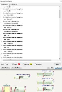
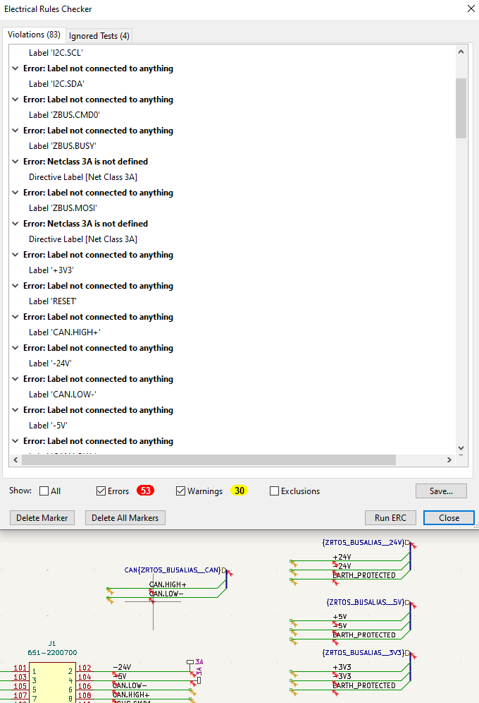
Electrical Rules Checker Fehlermeldungen in EDA-Software
: Label not connected to anything Label 'RESET' Error: Label not connected to anything Label 'CAN.HIGH+' Error: Label not connected to anything Label '-24V' Error: Label not connected to anything Label 'CAN.LOW-' Error: Label not connected to anything Label '-5V' Show: All Errors 53 Warnings 30 Exclusions Save... Run ERC Close J1 651-2200700 CAN[ZRTOS_BUSALIAS__CAN] CAN.HIGH+ CAN.LOW- {ZRTOS_BUSALIAS__24V} +24V EARTH_PROTECTED {ZRTOS_BUSALIAS__5V} +5V EARTH_PROTECTED {ZRTOS_BUSALIAS__3V3} +3V3 3V3 EARTH_PROTECTED 101 102 -4V 103 104 105 106 CAN.LOW- 107 108 CAN.HIGH+