mehr auf die 10mA aber bestimmt nicht tödlich für > die LED.... Doch. Vorwärts z.B. 2.1V bei 20mA = 0.042W, rückwärts 7V bei 20mA = 0.14W. Die Transil blockt jedoch nicht nur Überspannung ab, sondern auch Verpolung auf unter 0.7V. [pre] 12V--1k5--+--1k5--+ _|_ | Transil /_
Freilaufdiode zwischen die Pins geloetet aus, weil eine negative Spitze die LED kaputt macht. So eine BAS/BAV/BAW laesst sich ganz gut dazwischen klemmen und anloeten.
das Wissen. Wissen kann man sich aneignen. Ich dachte dafür gäb's diese Foren... Ich habe vor ca. 20 Jahren eine Ausbildung zum Elektroniker für Betriebstechnik begonnen und bin dann Ende des zweiten Lehrjahrs auf IT umgeschwenkt. Mein Wissen ist eingerostet aber das kann man auffrischen. Mein Interesse
Collector T1 (z.B. TIP41C) K2_A2 -> Collector T2 Emitter T1 -> Emitter T2 -> - Pol Solarbatterie Base T1 -> Arduino Digital Pin 1 Base T2 -> Arduino Digital Pin 2 Eingangspin am Arduino über einen 5V Trafo vom Wechselrichter speisen. Wenn Wechselrichter an ist, schaltet der Arduino K1, ansonsten
433.967 rechne nochmal die Ungenauigkeit drauf und dann...? Vordefiniere Filter sind ja z.B. 10kHz, 20kHz (Narrow, Wide, ...)? Und wie erklärt sich jetzt das "Problem" bei AM? Ist das eine inherente Problematik warum man dann eher FM verwenden würde?
abzusenken. Das bekommt "einfachen" Demodulatoren nicht besonders. Uebliche Werte liegen eher bei 20 - 30%. Zur Reichweiteoptimierung kann man auch noch hoehere Werte probieren.
. = 150 ABSOLUTE MAXIMUM RATINGS Symbol Parameter Value Unit NPN BDX53F PNP BDX54F VCBO Collector-Base Voltage EI = 0) 160 V VCEO Collector-Emitter VoltageB(I = 0) 160 V VEBO Emitter-base Voltage CI = 0) 5 V IC Collector Current 8 A CM Collector Peak Current 12 A IB Base Current 0.2 A o Ptot Total Dissipation
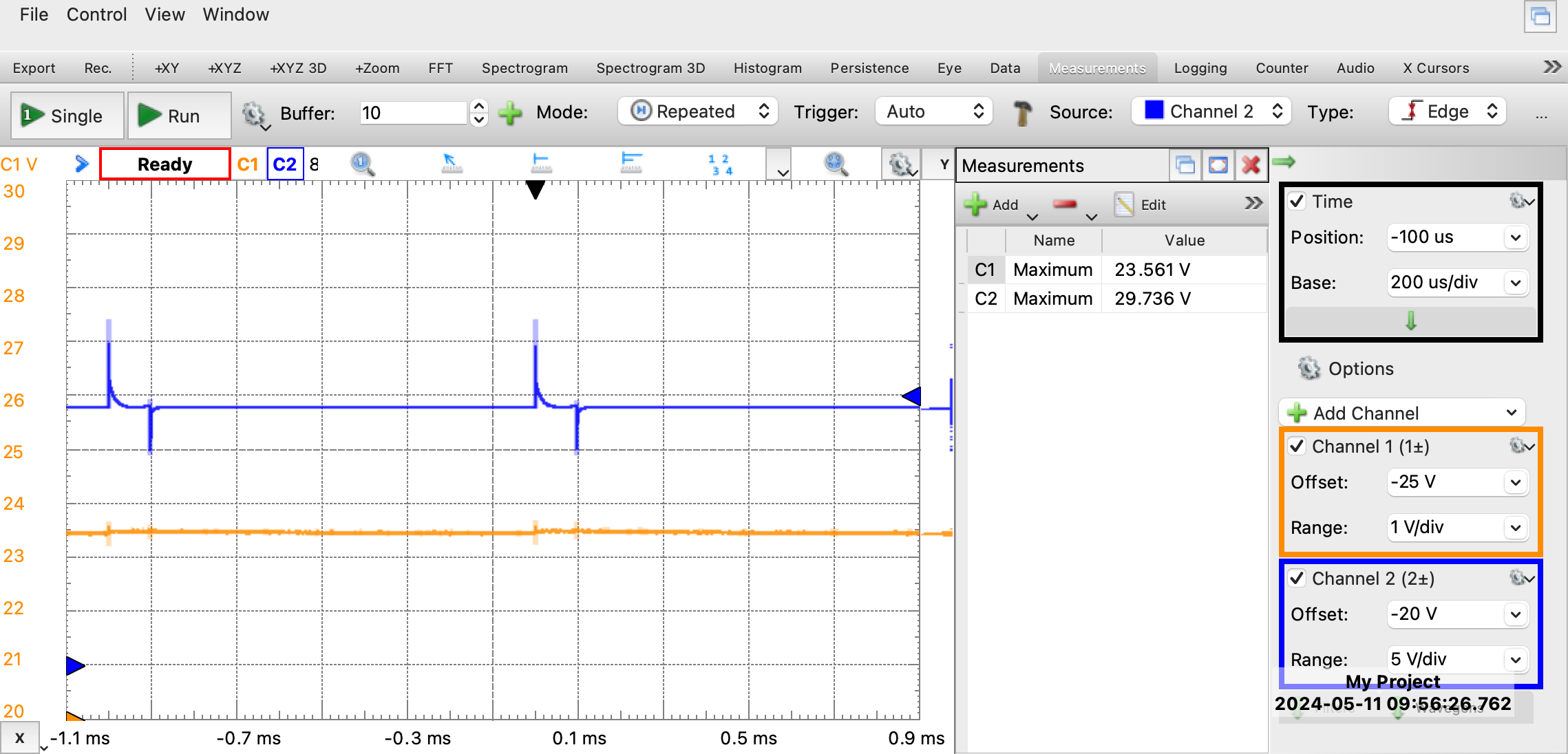
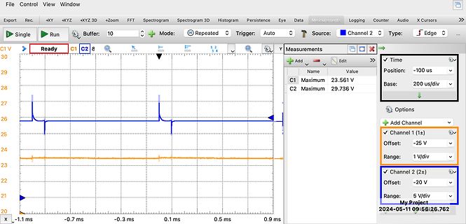
Y Measurements Add Edit Name Value C1 Maximum 23.561 V C2 Maximum 29.736 V Time Position: -100 us Base: 200 us/div Options Add Channel Channel 1 (1±) Offset: -25 V Range: 1 V/div Channel 2 (2±) Offset: -20 V Range: 5 V/div 2024-05-11 09:56:26.762
Transistortester, dessen Flash immer mehr aus allen Nähten platzt. https://www.eevblog.com/forum/testgear/$20-lcr-esr-transistor-checker-project/msg5054215/#msg5054215 https://www.eevblog.com/forum/testgear/$20-lcr-esr-transistor-checker-project/msg5150607/#msg5150607 Außerdem ist selbst der 8er deutlich
von /root . Output locations for built toolchains . target dir - modify to keep results BASE=${BASE:-/media/ab/Linux-HDD/avr-toolchain__/}
are defined as part of the port layer. THIS MUST BE THE SECOND MEMBER OF THE TCB STRUCT. */ ? BaseType_t xUsingStaticallyAllocatedStack; /* Set to pdTRUE if the stack is a statically allocated array, and pdFALSE if the stack is dynamically allocated. */ #endif 8 ListItem_t xGenericListItem
Pin Change Interrupt source 21: The PC5 pin can serve as an external interrupt source. • TDO/PCINT20 – Port C, Bit 4 TDO, JTAG Test Data Output. PCINT20, Pin Change Interrupt source 20: The PC4 pin can serve as an external interrupt source. • TMS/PCINT19 – Port C, Bit 3 TMS, JTAG Test Mode Select. PCINT19
// for extended speed ranges this should be defined #define FCY 20000000 // xtal = 5Mhz; PLLx16 -> 20 MIPS #define FPWM 20000 // 20 kHz, so that no audible noise is present. #define _10MILLISEC 10 // Used as a timeout with no hall effect sensors // transitions and Forcing steps according to the // actual
longer the only system Host. Can be a camera or a printer. 2 DesignCon 2003 TecForum I C Bus Overview 20 DesignCon 2003 TecForum I C Bus Overview 18 Slide 20 Slide 18 USB aims at mass-market products and design-ins may be less convenient for small users. The serial port is USB is the most complex of the
interrupts/events • One compare match per compare channel • Two 8-bit timer/counters in Split Mode 20.2 Overview The flexible 16-bit PWM Timer/Counter type A (TCA) provides accurate program execution timing, frequency and waveform generation, and command execution. A TCA consists of a base counter and
www.radiomuseum.org/r/werk_fern_verzoegerungsleitung_cv_1.html#images Danach kam dann die kleine CV20 mit Mehrfachreflektionen, wie man sie in vielen Farbdekodern vorgefunden hatte.
uploads%2Fpics%2F1967-wie-ein-farbbild-entsteht-Bild-0124.jpg&width=1280m&height=1024m&bodyTag=%3Cbody%20style%3D%22margin%3A0%3B%20background%3A%23fff%3B%22%3E&wrap=%3Ca%20href%3D%22javascript%3Aclose%28%29%3B%22%3E%20%7C%20%3C%2Fa%3E&md5=aca645f48f51c1568894cccf20c36bbc Interessant: Die Schemazeichnung
es der Prototyp des Autors auf MikroBasic bearbeiten, da diese bis zu 2 eine Stromaufnahme von nur 20 nA im 20 Personal Download for Hans-Jürgen Heidenreich | copyright Elektor ein Kunststoffgehäuse (am besten eines mit Batterie-Halterung). Man darf dann nur nicht das Loch für den Fototransistor vergessen
10mA Input Resistor Tolerance (Note 6) ∆R1 -30 +30 % - Resistance Ratio Tolerance (Note 6) ∆R2/R1 -20 +20 % - Gain-Bandwidth Product (Note 6) f 250 MHz V = 10V, I = 5mA, f = 100MHz T CE E Electrical Characteristics, Switching Diode @ T A 25°C unless otherwise specified Characteristic Symbol Min
Current 140 120 RMS limit ) ( s 100 o r 80 e o D = 0.01 P 60 D = 0.05 e D = 0.10 a 40 D = 0.20 e D = 0.50 A DC 20 0 0 20 40 60 80 100 I - Average Forward Current (A) F(AV) Fig. 5 - Average Power Loss vs. Average Forward Current 1 e ) n W a / e ( p e 0.1 I a a C m t 0.50 e n 0.20 T i 0.01 0.10
Parameter Device Typ. Max. Units Test Conditions λpeak Peak Wavelength High Efficiency Red 627 nm F=20mA Dominant Wavelength High Efficiency Red 625 nm F=20mA λD ∆λ1/2 Spectral Line Half-width High Efficiency Red 45 nm F=20mA C Capacitance High Efficiency Red 15 pF V F=0V;f=1MHz VF Forward Voltage High Efficiency Red 2.0 2.5 V F=20mA IR Reverse Current High Efficiency Red 10 uA V R= 5V Absolute Maximum Ratings at T A=25°C Parameter High Efficiency Red Units Power dissipation 105 mW DC Forward Current 30 mA Peak Forward Current
- VCE 30 V, - V =EB V - CBX – – 50 nA Emitter-Base cutoff current – Emitter-Basis-Reststrom - VCE 30 V, - V =EB V - EBV – –- 50 nA Gain-Bandwidth Product – Transitfrequenz - I = 10 mA, - V = 20 V, f = 100 MHz f 250 MHz – – C CE T Collector-Base Capacitance – Kollektor-Basis-Kapazität - VCB 5 V, I E i =e0, f = 1 MHz CCBO – – 4.5 pF Emitter-Base Capacitance – Emitter-Basis-Kapazität - VEB 0.5 V, I C i =c0, f = 1 MHz CEBO – – 10 pf Noise figure – Rauschzahl - VCE 5 V, - I C 100 µA, R = G kΩ, f = 1 kHz F – – 4 dB Switching times – Schaltzeiten
Länge eines Kabels hinweg stark gedämpft werden. Zum Beispiel die IEEE 802,3 Spezifikation für 1000BASE-T ermöglicht einen Verlust von maximal 24 dB, as zu einem Signal führt, das auf seiner Reise vom fernen Endsender zum Ethernet-Port Ihres Computers auf (ich werde die Mathematik für die Dichter erledigen
zu messen? Das Multimeter auch mal auf AC > schalten, das sollten dann 0V sein (Timebasestellung 20ms), nicht dass > die gemessene DC Spannung doch nur ein AC Mittelwert ist. An R3100 und an 3101 im XY Betrieb mit Timebase 20ms 2,45V mit DC gemessen, mit AC = 0V. Kann ich sweep out auch
Offenbar langsame Drift beim Aufwärmen nach oben; ansonsten 5V = 10cm. Ja, und gleiche Spannung an den Basen ist ziemlich genau Bildschirmmitte.
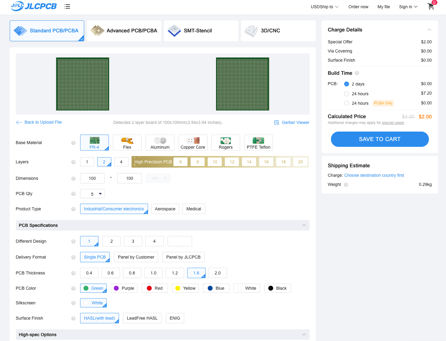
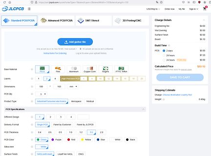
Offer $2.00 Via Covering $0.00 Surface Finish $0.00 Build Time 2 days $0.00 24 hours PCBA Only $7.20 24 hours Calculated Price $4.00 $2.00 SAVE TO CART Shipping Estimate Charge: Choose destination country first Weight 0.29kg Base Material FR-4 Flex Aluminum Copper Core Rogers PTFE Teflon Layers 1 2 4 High Precision PCB 6 8 10 12 14 16 20 Dimensions 100 * 100 mm PCB Qty 5 Product Type Industrial/Consumer electronics Aerospace Medical PCB Specifications Different Design 1 2 3 4 Delivery Format Single PCB Panel by Customer Panel by JLCPCB
Base64 U. schrieb im Beitrag #7638221: > Fingersicherheit ist doch stand der Technik oder so? > Schaut auch so aus als wär das in dem Video nach dem Zähler. Das ist eine Altanlage in GB.
500KW PV Anlage, direkt auf nen eigenen Trafo. Die UV Schränke sind abschließbar (ca, 1m Breit, 1,20 Hoch, die hälfte Anschlußraum).. hinter der Tür ist alles offen. Da gehen 2 Kabel a 5*240 ALU auf die Schienen. Wurde so abgenommen und fertig.
shape into a rectangular PWM output signal. Element 2NAND (Fig.20) is made on a chip 222 and a transistor VT1. ISSN: 2367-8879 26 Volume 6, 2021 International Journal of Circuits and Electronics M. A. Shustov http://www.iaras.org/iaras/journals/ijce Fig.20: Element
bleiben dann vor der Galvanik noch 15µm übrig und wenn du 20µm in die Hülse bekommen willst, dann bedeutet das, dass du fast das doppelte auf den Außenlagen aufkupferst. Wenn du dieses dann nicht rückätzt oder direkt mit 9µm oder 5µm Folie startest (was teurer
Trägerfolie verarbeitet werden können) hast du auf den Außenlagen mindestens 50µm Kupfer. (15µm + 20µm +20µm*80%) Startet man mit 35µm Folie, erhält man entsprechend 70µm auf den Außenlagen.
user population of about a dozen, most of them friends, and I didn't want to screw up my embedded base. The rest, sadly, is history." https://retrocomputing.stackexchange.com/questions/20292/why-does-make-only-accept-tab-indentation
kompletten Linuxkernel im Projekt hat, aber auch der lag IMHO so bei 5min und nicht mehr 30min wie vor 20Jahren. Und wie ich schon sagte, ueblicherweise wird ja immer nur eine Datei uebersetzt an der man halt gerade arbeitet. Vanye
number of PWM period samples to be taken for the plausibility check (see chapter 9.2). is the PWM base frequency. Therefore the time to go into PWM Quiescent current mode depends on the actual PWM base frequency and the number of samples for the plausibility check. Additionally 2 s are waited after the
L= 20p , R L= 100 k , 0°C 340 kHz OM See Figure 70°C 260 25°C 1.7 B1 Unity-gain bandwidth VI= 10 mV, C L 20 pF, See Figure 3 0°C 2 MHz 70°C 1.3 V = 10 mV, f = B, C = 20 pF, 25°C 46° φm Phase margin I 1 L 0
Collector-Emitter Leakage Current ICEO 5 50 nA VCE=10 V Collector-Emitter Saturation Voltage V 0.25 I =1 mA, I =20 A CESAT CE B Base-Emitter Voltage VBE 0.65 V VCE=10 V, B =20 A DC Forward Current Gain HFE 200 650 1800 VCE=10 V, B =20 A Saturated DC Forward Current Gain HFE SAT 120 400 600 VCE=0.4 V,BI =20 A Thermal
video 1. Remove drum and back part of housing. 2. Remove condensate pump. 3. Remove float from the base pan and remove fluff / deposits. 4. Remove fluff / deposits from area around condensate pump and float. 5. Detach front panel from the base group. Carefully detach seal from the base group between front panel and base group. 6. Remove diffuser and cover from the heat pump. 7. Lift heat pump out of the base group to be able to clean the front of the heat pump. 8. Remove partition from under the heat pump and clean
Aufmachung: "Former soviet union in14 glow tube watch, parts need to be assembled by yourself PCB base and board already update to this version two 1. Input: 11v 13 13v 1a dc power supply (5.5-2.1)" mfg
normalerweise 5V. Außerdem ein anderer Schaltregler links unten. Der Mikrocontroller dürfte der 20-pinner rechts außen sein, leider ist keine Bezeichnung zu erkennen. Ein paar Transistoren drumherum versorgen vielleicht noch die farbigen LEDs. Ein Quarz ist nicht zu sehen, aber die Uhr braucht auf
.) • Digital camera (Digital still camera) • Game equipment • LCD monitor, LCD modules • Wireless base station • Power supply • Medical device Electrical Specifications Current Voltage Interrupting Typical Cold Typical I T* Part Number Marking 2 Rating (A) Rating (V) Rating (V) DCR* (mΩ) (A s) S0603-
data set-up time 250 - 100 [5] - 50 - ns n SU;DAT R o tr rise time of both SDA and SCL signals - 1000 20 300 - 120 ns e e . n tf fall time of both SDA and SCL - 300 20 × 300 20 × 120 [8] ns 6 i [3][6][7][8] [9] — o signals (VDD / 5.5 V) (VDD / 5.5 V) 4 m t set-up time for STOP condition 4.0 - 0.6 - 0.26

 Bild
 Bild
 Bild