-
PDF
nFET_ZXM61N02FTA.pdf
Leakage IGSS 100 nA VGS=± 12V, VDS=0V Gate-Source Threshold Voltage V 0.7 V I =250 A, V = V GS(th) D DS GS Static Drain-Source On-State Resistance R 0.18 V =4.5V, I =0.93A DS(on) GS D (1) 0.24 VGS=2.7V, ID=0.47A Forward Transconductance (3) g fs 1.3 S VDS=10V,ID=0.47A DYNAMIC (3) Input Capacitance C iss
in „RaspiPi mit 3,3V einen 5V Kreis wie schalten?“ · Mikrocontroller und Digitale Elektronik ·
-
PDF
Infineon-IPD180N10N3_G-DS-v02_03-en.pdf
IPD180N10N3 G TM OptiMOS 3 Power-Transistor Product Summary Features V 100 V DS • N-channel, normal level RDS(on),max TO-263 18 mW • Excellent gate charge x DS(on)roduct (FOM) D 43 A • Very low on-resistance DS(on) • 175 °C operating temperature • Pb-free lead plating; RoHS compliant
in „MosFet; unterschiedliche Schaltzeiten aus Datenblatt und Simulation“ · Analoge Elektronik und Schaltungstechnik ·
-
PDF
NDP6020P.pdf
0.041 0.05 Ω T =125°C 0.06 0.08 J R StaticDrain-SourceOn-Resistance V = -2.7 V,I =-10 A 0.059 0.07 DS(ON) GS D R StaticDrain-SourceOn-Resistance V = -2.5 V, I =-10 A 0.064 0.075 DS(ON) GS D ID(on) On-StateDrainCurrent VGS-4.5 V,V =-DSV -24 A gFS ForwardTransconductance VDS-5 V,I =D12A 14 S DYNAMICCHARACTERISTICS
in „P-Channel High-Side Switch 3,3V“ · Mikrocontroller und Digitale Elektronik ·
-
PDF
MIC5233-3.3YS-microchip-20221000.pdf
FIGURE 2-9: Ground Pin Current vs. FIGURE 2-12: Ground Pin Current vs. Temperature. Input Voltage. DS20006033E-page 6 2018-2022MicrochipTechnologyInc.anditssubsidiaries MIC5233 FIGURE 2-13: Input Current vs. Supply FIGURE 2-16: Load Transient Response. Voltage. FIGURE 2-14: Output Voltage vs. Temperature
in „STM32F302C8T6 Schaltplanüberprüfung“ · Mikrocontroller und Digitale Elektronik ·
-
PDF
Infineon-ApplicationNote_Some_key_facts_about_avalanche-ApplicationNotes-v01_01-EN.pdf
performance technologies,inparticulartheproductofdrain-sourceon-stateresistancebyactive area,also knownas R DS(on)x A.Indeed,whereasatechnologyreductionof R DS(on)xAusuallyleadstosmaller chipsizesfor a defined R value, the deviceitselfrequires abiggerchip sizeinorder to mitigatethe temperature increase DS(on)
in „MOSFET Avalanche rated“ · Analoge Elektronik und Schaltungstechnik ·
-
PDF
Infineon-ApplicationNote_Some_key_facts_about_avalanche-ApplicationNotes-v01_01-EN.pdf
performance technologies,inparticulartheproductofdrain-sourceon-stateresistancebyactive area,also knownas R DS(on)x A.Indeed,whereasatechnologyreductionof R DS(on)xAusuallyleadstosmaller chipsizesfor a defined R value, the deviceitselfrequires abiggerchip sizeinorder to mitigatethe temperature increase DS(on)
in „SMD Mosfet mit Z-Diode für induktive Last“ · Analoge Elektronik und Schaltungstechnik ·
-
PDF
1-SPD30N06S2L-13_1-1.pdf
d e f g h i 5 3.4 3.6 3.84.0 4.57.0 10.0 0 0 0 0.5 1 1.5 2 2.5 3 3.5 4 V 5 0 10 20 30 40 50 A 65 V DS ID 7 Typ. transfer characteristics 8 Typ. forward transconductance I = f ( V ); V ‡ 2 x I x R g = f(I ); T =25°C D GS DS D DS(on)max fs D j parameter: t = p0 µs parameter: g fs 60 70 A S 50 45 50 40
in „Kuehlkoerper“ · Mikrocontroller und Digitale Elektronik ·
-
PDF
PMBFJ620_1.pdf
= 0 V 24 - 60 mA IGSS gate-source leakage current VGS = −15 V; DS = 0 V - - −1 nA R DSon drain-source on-state VGS = 0 V; DS = 100 mV - 50 - resistance yfs common source forward D = 10 mA; VDS = 10 V 10 - - mS transfer admittance yos common source output D = 10
in „Doppelfet für Vorstufe“ · Analoge Elektronik und Schaltungstechnik ·
-
PDF
MTE011N10RFP-CystechElectonics.pdf
MTE011N10RFP BV DSS 100V ID@V GS=10V, TC=25°C 34A Features ID@V GS=10V, TA=25°C 9A Low On Resistance R DS(ON@V GS=10V, ID=11A 11 mΩ(typ) Simple Drive Requirement Low Gate Charge Fast Switching Characteristic Insulating package, front/back side insulating voltage=2500V(AC) RoHS compliant package
in „IC identifizieren“ · Analoge Elektronik und Schaltungstechnik ·
-
PDF
LTC4414_Power_Manegement.pdf
= 0V –10 –1 1 µA LEAK IN IN When Other Pin Supplies Power VIN= 14V, SENSE = –14V –10 1 µA VIN= 36V, SENSE = 8V –10 1 µA VIN 0V, SENSE = 28V –10 1 µA VIN= –14V, SENSE = 14V –10 1 µA VIN= 8V, SENSE = 36V –10 1 µA PowerPath Controller VFR PowerPath Switch Forward Regulation
in „P-Mosfet als Schalter“ · Analoge Elektronik und Schaltungstechnik ·
-
PDF
IRLU2905.pdf
175°C 1 1 0.1 1 10 100 0.1 1 10 100 V , Drain-to-Source Voltage (V) V , Drain-to-Source Voltage (V) DS DS Fig 1. Typical Output Characteristics Fig 2. Typical Output Characteristics 1000.0 60 ) Α TJ= 25°C ( 50 T J 175°C ( e n n r t u100.0 T J 175°C u 40 C n r c u s 30 TJ= 25°C S r t T n 10.0 r a a 20
in „Batterieschutzschaltung. Murks oder möglich?“ · Analoge Elektronik und Schaltungstechnik ·
-
PDF
Datenblatt.pdf
g(TH) V GS = 0 to 2V (Figure 13) - 3.7 4.5 nC Input Capacitance C V = 25V, V = 0V - 2020 - pF ISS DS GS Output Capacitance C f = 1MHz - 600 - pF OSS (Figure 12) Reverse Transfer Capacitance C - 200 - pF RSS Thermal Resistance Junction to Case R θJC (Figure 3) - - 1.14 oC/W Thermal Resistance Junction
in „Motorensteuerung Raspberry PI“ · Mikrocontroller und Digitale Elektronik ·
-
PDF
Class_1_Bluetooth_Module_with_EDR_Support_DS500022-2257897.pdf
Quicker Time to Market • Compatible with Microchip Microcontroller Fami- lies (PIC16F, PIC18F, PIC24F/H, dsPIC33 and PIC32) • Up to 100 meter range 2021 Microchip Technology Inc. DS50002280B-page 1 RN41/RN41N RN41/RN41 MODULE VARIANTS (1) Model Antenna Firmware Description RN41 Ceramic Chip 4.77, 6.15 Class
in „[V] Microchip Bluetooth Module RN41-I/RM und RN42-I/RM“ · Markt ·
-
Datei
ON_OFF.bas
Display ' Hier jetzt noch der Geist Spidata = T_st(n_2) Call Sendspi2display(spidata) Next N_1 Dog_ds = 0 Dispadr = &B10000000 + 16 ' Wir schreiben erst mal in die Grossen Zeichen Call Sendspi2display(dispadr) ' Schreibposition waehlen Dog_ds = 1 ' Jetzt kommen wirkliche Zeichen! For N_1 = 1 To 16 N_
in „Noch ein Taschenrechner auf ATMega Basis“ · Projekte & Code ·
-
PDF
MCP73811_2.pdf
Charge Current I 90 100 110 mA PROG = 10 kΩ REG Regulation 450 505 550 mA PROG = 2.0 kΩ, Note 1 12.5 14.5 16.5 mA PROG = 67 kΩ T = -5°C to +55°C A Note 1: Not production tested. Ensured by design. 2005-2013 Microchip Technology Inc. DS20001984F-page 3 MCP73831/2 DC CHARACTERISTICS (CONTINUED) Electrical
in „Hackbarer(?) 21 EUR Quadcopter“ · Mikrocontroller und Digitale Elektronik ·
-
PDF
MCP_73831.pdf
Charge Current I 90 100 110 mA PROG = 10 kΩ REG Regulation 450 505 550 mA PROG = 2.0 kΩ, Note 1 12.5 14.5 16.5 mA PROG = 67 kΩ T = -5°C to +55°C A Note 1: Not production tested. Ensured by design. 2005-2013 Microchip Technology Inc. DS20001984F-page 3 MCP73831/2 DC CHARACTERISTICS (CONTINUED) Electrical
in „LiPo-IC MCP73831 kennt keine Ladeschlussspannung“ · Analoge Elektronik und Schaltungstechnik ·
-
PDF
MRF89XAM8A.pdf
IC. DS70651A-page 14 Preliminary © 2010 Microchip Technology Inc. MRF89XAM8A FIGURE 2-11: PCB ANTENNA SIMULATION DRAWING FIGURE 2-12: SIMULATED 2D RADIATION PATTERN © 2010 Microchip Technology Inc. Preliminary DS70651A-page 15 MRF89XAM8A FIGURE 2-13: SIMULATED 3D RADIATION PATTERN FIGURE 2-14: SIMULATED PCB ANTENNA IMPEDANCE DS70651A-page 16 Preliminary © 2010 Microchip Technology Inc. MRF89XAM8A FIGURE 2-15:
in „Was darf man von einer PCB-Antenne erwarten?“ · HF, Funk und Felder ·
-
PDF
SST89x516.pdf
ERAM address within 0 to 0FFH; cannot access 100H to 02FFH. ©2013 Silicon Storage Technology, Inc. DS25093B 02/13 14 FlashFlex MCU SST89E516RD2 / SST89E516RD SST89V516RD2 / SST89V516RD Data Sheet 2FFH FFH Expanded (Indirect Addressing)FFH (Direct Addressing) RAM 768 Bytes Special Function Registers Upper
in „Einstieg in 8051 - Atmels AT89S52 oder?“ · Mikrocontroller und Digitale Elektronik ·
-
PDF
irl2203n.pdf
GS D ––– ––– 10 VGS= 4.5V, D = 48A V Gate Threshold Voltage 1.0 ––– ––– V V = V , I = 250µA GS(th) DS GS D gfs Forward Transconductance 73 ––– ––– S VDS= 25V, D = 60A ––– ––– 25 V = 30V, V = 0V DSS Drain-to-Source Leakage Current µA DS GS ––– ––– 250 VDS= 24V, VGS = 0V, J = 125°C Gate-to-Source Forward
in „Saito Pro Charger Batterieladegerät - Mikrocontroller ATmel ATTINY26L defekt?“ · Mikrocontroller und Digitale Elektronik ·
-
PDF
MOSFET_Gate_Driver_Circuit.pdf
best suits your system requirements. Figure 4.2 I – V Figure 4.3 R vs. Figure 4.4 V -V curves D GS DS(ON) DS GS curves temperature © 2017 - 2018 14 2018-07-26 Toshiba Electronic Devices & Storage Corporation MOSFET Gate Drive Circuit Application Note 4.2. Gate voltage, peak current and drive loss In
in „MOSFET npn/pnp Driver“ · Analoge Elektronik und Schaltungstechnik ·
-
PDF
MOSFET_Gate_Drive_Circuit_.pdf
best suits your system requirements. Figure 4.2 I – V Figure 4.3 R vs. Figure 4.4 V -V curves D GS DS(ON) DS GS curves temperature © 2017 - 2018 14 2018-07-26 Toshiba Electronic Devices & Storage Corporation MOSFET Gate Drive Circuit Application Note 4.2. Gate voltage, peak current and drive loss In
in „Gatebeschaltung Treiber“ · Analoge Elektronik und Schaltungstechnik ·
-
PDF
FDP060AN08A0.pdf
Drain to Source Breakdown Voltage D = 250µA, GS = 0V 75 - - V 0 6 I Zero Gate Voltage Drain Current V DS = 60V - - 1 µA A DSS V GS= 0V TC= 150 C - - 250 N 0 IGSS Gate to Source Leakage Current V GS= ±20V - - ±100 nA 8 A On Characteristics 0 — VGS(TH) Gate to Source Threshold Voltage V GS= V DS,DI = 250µA
in „Simulation IR2183 Halbbrückentreiber“ · Analoge Elektronik und Schaltungstechnik ·
-
PDF
12887.pdf
– +5 Volt Supply – End of clock update cycle GND – Ground DESCRIPTION The DS12887 Real Time Clock plus RAM is designed to be a direct replacement for the DS1287. The DS12887 is identical in form, fit, and function to the DS1287, and has an additional 64 bytes of general purpose
in „Anschluss von AT89C55WD“ · Mikrocontroller und Digitale Elektronik ·
-
PDF
Projekt_Hausautomation-Temperatursensoren.pdf
1 2 3 4 5 6 +3.3V A A Temperaturerfassung 1 J7 2 Power 3.3V 3 D 2 V U4 DQ D N DS18B20 G 1 1 1 2 2 3 3 4 4 5 5 3 J12 J116 7 7 D 2 V U5 8 8 DQ D DS18B20 9 9 G 10 10 1 B 11 11 B 12 12 3 Temperatursensoren DS18b20 D 2 V U6 U3 DQ D DS18B20 GND G NodeMCU1.0(ESP-12E) R6 1 3,3k 1 A0(ADC0
in „ESP8266 mehrere Temperaturfühler mit Display“ · Mikrocontroller und Digitale Elektronik ·
-
Datei
tester2.asm
slaves+vorbereitung der tempmessung rcall read_scratchpad rcall ds_reset rcall ausgabe ret ;****************adr auslesen eines einzelnen sensors**************** ds18_rr:rcall ds_reset ;wer ist da??? rcall read_rom rcall ds_reset ;wer ist da??? rcall ausgabe3 ret ;**
in „ds1820 befehle“ · Mikrocontroller und Digitale Elektronik ·
-
PDF
DG506_507_508_509A.pdf
1 16 A1 A0 1 16 A1 NC 2 27 V- DB 2 27 V- EN 2 15 A2 EN 2 15 GND NC 3 26 S8 NC 3 26 S8A V- V+ V- 3 14 GND 3 14 S16 4 25 S7 S8B 4 25 S7A S S S 1 4 13 V+ 1A 4 13 1B S15 5 24 S6 S7B 5 24 S6A S2 5 12 S S2A 5 12 S S 6 23 S S 6 23 S 5 2B 14 5 6B 5A S3 6 11 S6 S3A 6 11 S3B S13 7 22 S4 S5B 7 22 S4A S4 7 10 S7
in „Bestimmtes Bauteil gesucht zur Signalverteilung“ · Mikrocontroller und Digitale Elektronik ·
-
PDF
BMA423.pdf
Supply I Nominal V and 3.5 µA DDsum DD Current in VDDIO, 25°C Suspend Mode Total Supply I Nominal V and 14 µA DDlp1 DD Current in VDDIO, 25°C Low-power Mode 50 Hz ODR Power-Up Time ts_up 1 ms Non-volatile nNVM 15 cycles memory (NVM) write-cycles BST-BMA423-DS000-00 | Version 1.0 | August 2017 Bosch Sensortec
in „LilyGo T-Watch 2020 v1 Micropython“ · Mikrocontroller und Digitale Elektronik ·
-
PDF
Temperatursensor.pdf
remain at a low logic level the transaction. for a minimum of one smicrosecond; output data from the DS1821 is then valid for the next 14 s maximum. Write Time Slots The host therefore must stop driving the DQ pin low in A write time slot is initiated when the host pulls the data ordertoreaditsstate15
-
Datei
ds1620.c
#include "ds1620.h" #include <util/delay.h> unsigned char ds1620_init (void) { /*set all pins as output*/ DDR_DS1620 = (1<<DQ_DS1620) | (1<<CLK_DS1620) | (1<<RES_DS1620); /*set CPU use bit, continuously temperature
in „DS1620 - Initialisierung zumTH und TL schreiben?“ · Mikrocontroller und Digitale Elektronik ·
-
PDF
e2928_a8v-vm_se.pdf
A B 256MB Mosel V826632K24SATG-D3 Mosel SS V58C2256804SAT5 • • 512MB Mosel V826664K24SATG-D3 Mosel DS V58C2256804SAT5 • • 256MB Nanya NT256D64S88B1G-5T Nanya SS NT5DS32M8BT-5T • • 512MB Nanya NT512D64S8HB1G-5T Nanya DS NT5DS32M8BT-5T • • 512MB Nanya NT512D64S88C0GY-5T Nanya SS NT5DS64M8CS-5T • • 1G Nanya
-
Datei
harware_config_default.txt
27) // 2. dsPICDEM Vdd <- PICtail VPIC (PICtail pin 25) // 3. dsPICDEM RG2 -> PICtail ENC28J60 CS (PICtail pin 22) // 4. dsPICDEM RF6 -> PICtail SCK (PICtail pin 11) // 5. dsPICDEM RF7 <- PICtail SDI (PICtail pin
in „I/O Pins konfigurieren“ · Mikrocontroller und Digitale Elektronik ·
-
PDF
NDS356AP.pdf
D -250 µA -0.8 -1.6 -2.5 V T J125°C -0.5 -1.3 -2.2 R DS(ON) Static Drain-Source On-Resistance VGS -4.5 V, ID= -1.1 A 0.25 0.3 Ω T J125°C 0.35 0.4 VGS -10 V, ID= -1.3 A 0.14 0.2 I On-State Drain Current V = -4.5 V, V = -5 V -3 A D(ON) GS DS g ForwardTransconductance
in „nds355/nds356“ · Markt ·
-
PDF
CY8C4147AZI.pdf
– 25 µs – Usable Deep Sleep Mode 2 is lowest current range. Mode Mode 1 has higher GBW. I – – SID_DS_1 DD_HI_M1 Mode 1, High current 1400 25 °C I – – SID_DS_2 DD_MED_M1 Mode 1, Medium current 700 25 °C SID_DS_3 I Mode 1, Low current – 200 – 25 °C DD_LOW_M1 µA SID_DS_4 IDD_HI_M2 Mode 2, High current
-
PDF
sihld24_Mosfet.pdf
PRODUCT SUMMARY • Dynamic dV/dt Rating VDS (V) 60 Available R () V = 5.0 V 0.10 For Automatic Insertion DS(on) GS RoHS* Qg(Max.) (nC) 18 End Stackable COMPLIANT Logic-Level Gate Drive Qgs (nC) 4.5 Qgd (nC) 12 R DS(on)Specified at VGS = 4 V and 5 V Configuration Single 175 °C Operating Temperature D Fast Switching
in „Mosfet sperrt nicht“ · Analoge Elektronik und Schaltungstechnik ·
-
Datei
diagramm.asm
max. Gr áe der Datei pop ds ;Datensegment restaurieren mov dx,0 ;Offsetadresse des Puffers int 21h push ds ;Datensegment retten mov dx,cs mov ds,dx mov si,offset hinweis2 mov di,beginhinweis2 mov cx,hinweis2laenge PR000: movsb
-
PDF
IXFH13N50.PDF
Switched-modeandresonant-mode V DSS VGS = 0 V, D = 250 mA 500 V V V = V , I = 2.5 mA 2 4 V powersupplies GS(th) DS GS D ● DC choppers ● Temperatureandlightingcontrols IGSS VGS = ±20 VDC V DS= 0 ±100 nA ● Low voltage relays IDSS VDS = 0.8 • DSS T J 25°C 200 mA V = 0 V T = 125°C 1 mA Advantages GS J ● Easy to mount
in „Betriebsstrom des MOSFET“ · Analoge Elektronik und Schaltungstechnik ·
-
PDF
IXFH13N50.PDF
Switched-modeandresonant-mode V DSS VGS = 0 V, D = 250 mA 500 V V V = V , I = 2.5 mA 2 4 V powersupplies GS(th) DS GS D ● DC choppers ● Temperatureandlightingcontrols IGSS VGS = ±20 VDC V DS= 0 ±100 nA ● Low voltage relays IDSS VDS = 0.8 • DSS T J 25°C 200 mA V = 0 V T = 125°C 1 mA Advantages GS J ● Easy to mount
in „Wie heiß wird mein MOSFET“ · Analoge Elektronik und Schaltungstechnik ·
-
PDF
IXFH13N50.PDF
Switched-modeandresonant-mode V DSS VGS = 0 V, D = 250 mA 500 V V V = V , I = 2.5 mA 2 4 V powersupplies GS(th) DS GS D ● DC choppers ● Temperatureandlightingcontrols IGSS VGS = ±20 VDC V DS= 0 ±100 nA ● Low voltage relays IDSS VDS = 0.8 • DSS T J 25°C 200 mA V = 0 V T = 125°C 1 mA Advantages GS J ● Easy to mount
in „Puls weiten modulation“ · Analoge Elektronik und Schaltungstechnik ·
-
PDF
ssr2n60a.pdf
MOSFET SSR/U2N60A FEATURES BV DSS = 600 V Avalanche Rugged Technology Rugged Gate Oxide Technology R DS(on) = 5 Ω Lower Input Capacitance I = 1.8 A Improved Gate Charge D Extended Safe Operating Area D-PAK I-PAK Lower Leakage Current : 25 μA (Max.) @ V DS = 600V Lower R : 3.892 Ω (Typ.) 2 DS(ON) 1 12 3
in „Ersatz für SSR2N60A“ · Analoge Elektronik und Schaltungstechnik ·
-
PDF
DS_UJ3N120070K3S-1530204.pdf
Static Parameter Symbol Test Conditions Value Units Min Typ Max Drain-source breakdown voltage BV DS V GS- 20V, ID=1mA 1200 V V DS1200V, 5 30 VGS -20V, T J 25°C Total drain leakage current D mA V DS1200V, 18 V GS-20V, T J 175°C V =-20V, T=25°C 5 50 Total gate leakage current G GS j mA V GS20V, T=j75
in „SiC Kaskoden Body Diode“ · Analoge Elektronik und Schaltungstechnik ·
-
PDF
AN162.pdf
the DS18X20/DS1822 1-Wire® temperature sensor in a microcontroller environment Abstract: This application introduces the user to simple 1-Wire software for interfacing a microcontroller to the DS18B20, DS18S20
in „Temperaturfühler identifizieren“ · Analoge Elektronik und Schaltungstechnik ·
-
PDF
DS90LV047A.pdf
D S January 2003 9 0 V 0 4 DS90LV047A A 3V LVDS Quad CMOS Differential Line Driver 3 V General Description Features L The DS90LV047A is a quad CMOS flow-through differential Mbps (200 MHz) switching rates V line driver designed for
in „TFT Display 8bit 16bit 8080 Interface über LVDS“ · Mikrocontroller und Digitale Elektronik ·
-
PDF
DS90LV047A.pdf
D S January 2003 9 0 V 0 4 DS90LV047A A 3V LVDS Quad CMOS Differential Line Driver 3 V General Description Features L The DS90LV047A is a quad CMOS flow-through differential Mbps (200 MHz) switching rates V line driver designed for
in „Analogsignal über Twisted-Wire übertragen“ · Analoge Elektronik und Schaltungstechnik ·
-
PDF
Littelfuse_Discrete_MOSFETs_N-Channel_Standard_IXT_1N450HV_Datasheet.PDF.pdf
Typ. Max. Easy to Mount J Space Savings V V = V , I = 250A 3.5 6.0 V High Power Density GS(th) DS GS D I V = 20V, V = 0V 100 nA GSS GS DS IDSS VDS = 3.6kV, VGS 0V 5 A Applications V DS= 4.5kV 25 μA V = 3.6kV T = 100C 15 μA DS J High Voltage Power Supplies R V = 10V, I = 50mA, Note 1 80 Capacitor Discharge Applications DS(on) GS D Pulse Circuits Laser and X-Ray Generation Systems © 2014 IXYS CORPORATION, All Rights Reserved DS100500D(04/14) IXTT1N450HV IXTH1N450HV Symbol Test Conditions Characteristic Values TO-268HV
in „SOA Diagramm richtig anwenden“ · Analoge Elektronik und Schaltungstechnik ·
-
 Bild
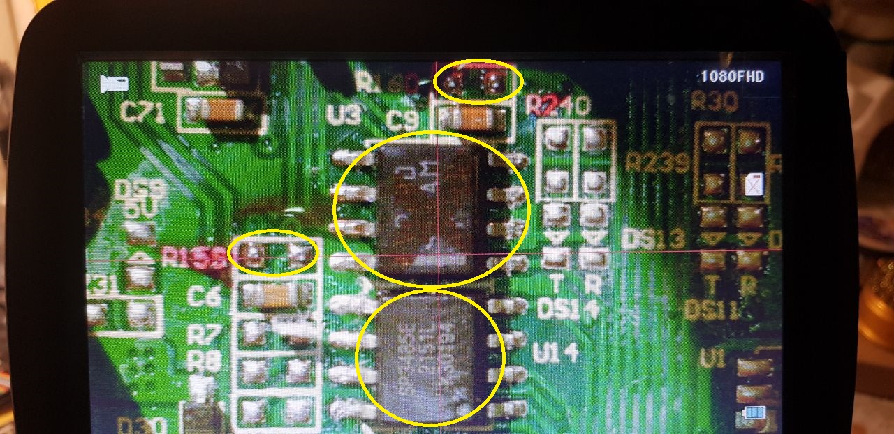
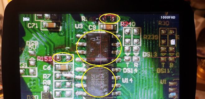
Mikroskopische Aufnahme einer Leiterplatte mit Bauteilen
C71 U3 C9 R240 R30 DS9 R239 DS13 R155 C6 DS14 R7 R8 U14 DS11 R8 U1 1080FHD
in „ALLPOWERS S2000 PRO Reparaturhilfe“ · Mikrocontroller und Digitale Elektronik · · Fotos
-
PDF
MOSFET_N_Dual_DMT3020LSD_LowRDS_SOIC8.pdf
Guaranteed by design. Not subject to product testing. DMT3020LSD 2 of 7 March 2018 Document number: DS40661 Rev. 2 - 2 www.diodes.com © Diodes Incorporated DMT3020LSD 30.0 20 VGS= 4.0V 18 VDS 5V 25.0 16 ) V GS= 10.0V A ( ( 14 T20.0 VGS= 4.5V N E V = 3.5V E 12 R GS R T U15.0 U 10 C C C O I I 8 U A VGS=
in „Unerwünschter Peak beim Ausschalten eines Kleinsignal-MOSFET“ · Analoge Elektronik und Schaltungstechnik ·
-
PDF
ds1308.pdf
Note 13: CBis the total capacitance of one bus line, including all connected devices, in pF. Note 14: The parameter t is the period of time the oscillator must be stopped for the OSF flag to be set over the voltage range of 2.4V P V P VF . CC CCMAX 2 Note 15: The DS1308 can detect any single SCL clock
in „[V] kleines Konvolut ältere DIL / DIP ICs (8€)“ · Markt ·
-
PDF
70687A-1.pdf
that the voltage requirements for the RF transceivers are met throughout the lifetime of the battery. DS70687A-page 14 2012 Microchip Technology Inc. MiWi™ DEMO KIT USER’S GUIDE Chapter 3. Getting Started This chapter is a self paced tutorial to use the MiWi™ Demo Board. It explains in detail how to run
in „Was darf man von einer PCB-Antenne erwarten?“ · HF, Funk und Felder ·
-
Datei
main.c
=!input(DS1820_DATA); delay_us(240); if(present) { return(TRUE); } else { return(FALSE); }//end if } void ds1820_read_rom(int *ptr) { int i; for(i=1;i<=64;i++) { output_low(DS1820_DATA); delay_us(14); output_float
in „PIC 16F690 RAM-Speicher“ · Mikrocontroller und Digitale Elektronik ·
-
PDF
AY0438a.pdf
output Clock Load FIGURE 7: CASCADETIMING DIAGRAM 1/f CLOCK 1 63 64 START Data in SEG 64 SEG 2 SEG 1 DS tDH Data out PD Load PW 1995 Microchip Technology Inc. DS70010I-page 3 AY0438 1.4 General 1.5 Interfacing to a LCD Module and PIC16CXX Device In order to avoid any race conditions, the Data In and Load
in „Suche Datenblatt HC0438A“ · Mikrocontroller und Digitale Elektronik ·