-
 Bild
Bild
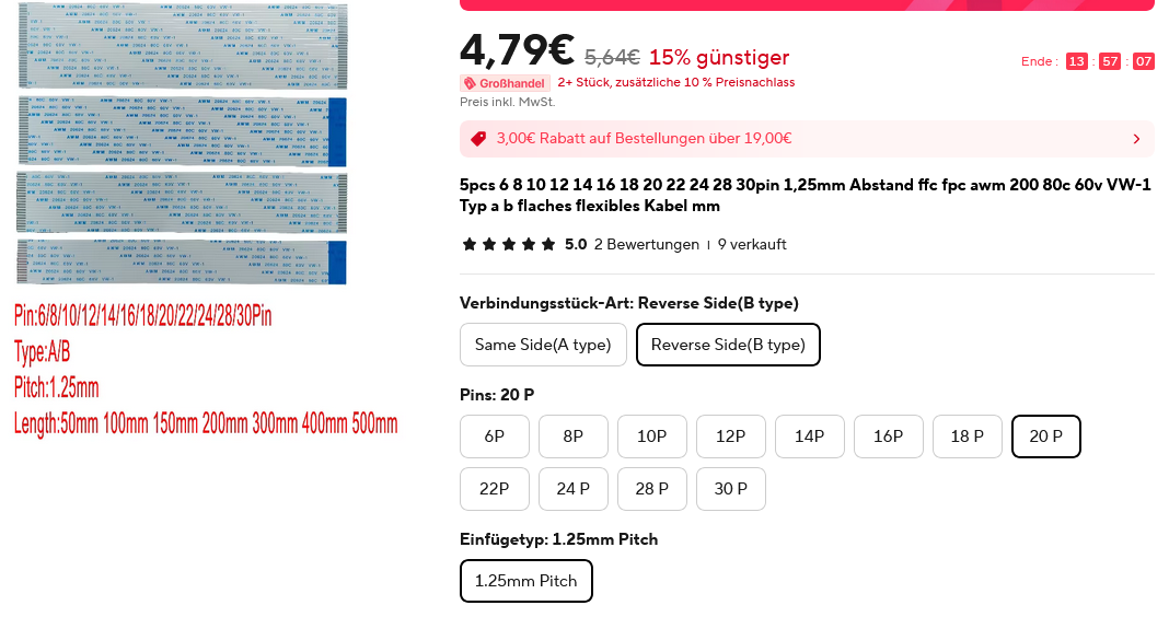
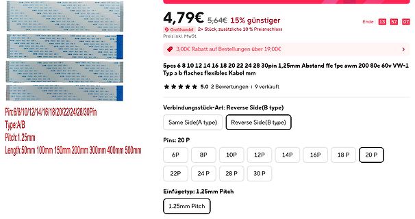
Screenshot eines Online-Shops für FFC-Flachbandkabel
VW-1 Typ a b flaches flexibles Kabel mm 5.0 2 Bewertungen 9 verkauft Verbindungsstück-Art: Reverse Side(B type) Same Side(A type) Reverse Side(B type) Pins: 20 P 6P 8P 10P 12P 14P 16P 18 P 20 P 22P 24 P 28 P 30 P Einfügetyp: 1.25mm Pitch 1.25mm Pitch
in „Buchsenleiste gesucht“ · Analoge Elektronik und Schaltungstechnik · · Screenshots
-
 Bild
Bild
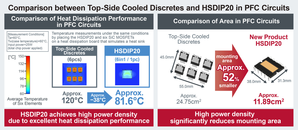
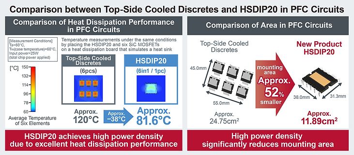
Vergleich Top-Side Cooled Discretes vs HSDIP20
Comparison between Top-Side Cooled Discretes and HSDIP20 in PFC Circuits Comparison of Heat Dissipation Performance in PFC Circuits [Measurement Conditions] Ta=60°C, Tw(case temperature)=60°C, Input power=25W (total chip power applied) Top-Side Cooled Discretes (6pcs) Approx. 120°C HSDIP20 (6in1 / 1pc) Approx. 81.6°C Comparison of Area in PFC Circuits Top-Side Cooled Discretes 45.0mm 55.0mm Approx. 24.75cm² New Product HSDIP20 mounting area
in „Digitalkamera auf Basis von ESP32-P4, neue ST-Audiosoftware uvam“ · Mikrocontroller und Digitale Elektronik · · Diagramme
-
PDF
ADUC7019_7020_7021_7022_7024_7025_7026_7027_7028.pdf
side switches. Therefore, independent control of this mode for in single update mode. In double update mode, the PWMEN both high-side and low-side switches is included with two register can also be updated
-
PDF
Infineon-Evaluation_Board_EVAL-1EDx20H12AH-SIC-ApplicationNotes-v01_00-EN.pdf
thegalvanic isolatedDC-DC convertertogenerate the isolated supply VCC2_Tand VEE2_T tosupplythehigh side driver and VCC2_B and VEE2_B tosupply thelow sidedriver. Onthelefthand side the generatorpartwiththeIC7IR2085SPBF is displayed. It's workingin combinationwith transistors BSL306N ashalf bridgeT8AandT8B
in „H-Brücke funktioniert nur mit Tastkopf“ · Mikrocontroller und Digitale Elektronik ·
-
Datei
main.py
args, **kwargs) self.btn = T.Button(self, text=f'Name_{index}', command=self.onclick) self.btn.pack(side=T.TOP) def onclick(self, event=None): print('%s called on %s'%(event, self.index)) class MainWin(T.Tk): def __init__(self, *args, **kwargs): super().__init__(*args, **kwargs) self.btns = [BtnFrame(self, i, *args, **kwargs) for i in range(5)] for btn in self.btns: btn.pack(side=T.TOP) self.btnExit = T.Button(self, text='Exit', command=self.destroy) self.btnExit.pack(side=T.BOTTOM) if __name__ == '__main__': MainWin().mainloop()
in „Kopien von tkinter-Frames erstellen und auswerten (python)“ · Softwareentwicklung ·
-
PDF
tsw-965282.pdf
18,52 B-CoOFF CW CCW Numbers of detent : 24 Pulse/Rotation : 12 pulse/360˚ ø21 PCB LAYOUT / COMPONENT SIDE +0.05 ø3 NO 18,52 4x ø 1,3 9 2 NO , 1 1 9 A COM B 3 0 , 4,50 +0.05 , 1 9 9,26 2x ø 1,6 0 B Dimensions arshown:m Specifications and dimensions subject to change www.ck-components.com C-3 TSW Series 3
-
PDF
WM8731.pdf
SIDETONE (ON) VMID BYPASS (OFF) FLINE INPUTS DACSEL (OFF) FROM DAC LINEOUT VMID HPOUT VMID Figure 24 Side Tone Mode Schematic REGISTER BIT LABEL DEFAULT DESCRIPTION ADDRESS 0000100 5 SIDETONE 0 Side Tone Switch (Analogue) Analogue 1 = Enable Side Tone Audio Path 0 = Disable Side Tone Control 7:6 SIDEATT[1:0] 00 Side Tone Attenuation 11 = -15dB 10 = -12dB 01 = -9dB 00 = -6dB Table 11 Side Tone Mode Table PD, Rev 4.8, April 2009 w 33 WM8731 / WM8731L Production Data The side tone mode and attenuation is selected
in „Deemphasis bei Audio-DAC“ · Mikrocontroller und Digitale Elektronik ·
-
PDF
Current_Sensing_Rev.1.1.pdf
We can distinguish between two possible insertion points of this resistor, the first being as low-side, the second as high-side shunt. U1 R shuntU2 R 1 R 2 R 3 R2 A digital R1 + D + output A digital D output I Ø R 4 I Ø U1 Rshunt U 2 Figure 1 Current measurement using low-side shunt (left) and high-side shunt resistor (right). Low-Side Current Shunt Resistor As shown in Figure 1, a low-side shunt resistor has one terminal connected to the battery ground ( U1 ), the other one connected to the load. An opamp setup is used with two resistors
in „TLE4998 - 5V/10V Schnittstelle über 7810?“ · Mikrocontroller und Digitale Elektronik ·
-
PDF
MAX5035-Datasheet.pdf
with a low ESR capacitor as close to the device as possible. 8 LX Source Connection of Internal High-Side Switch Block Diagram ON/OFF VIN ENABLE REGULATOR 1.69V (FOR ANALOG) CPFM REF-PFM HIGH-SIDE CURRENT REGULATOR CILIM SENSE VD (FOR DRIVER) VREF OSC RAMP REF-LIM BST MAX5035 FB CLK CONTROL RAMP LOGIC Rh
in „KICAT Footprint SO8E oder SO8N“ · Mikrocontroller und Digitale Elektronik ·
-
PDF
MP1584.pdf
Range switching regulator with an integrated internal • Up to 1.5MHz Programmable Switching high-side high voltage power MOSFET. It Frequency provides 3A output with current mode control for • High-Efficiency Pulse Skipping Mode for fast loop response and easy compensation. Light Load The wide 4.5V
in „COMP PIN MP1584“ · Mikrocontroller und Digitale Elektronik ·
-
PDF
NL6448AC30-12.pdf
150 : 1 (typ.) Viewing angle (more than the contrast ratio of 10 : 1) ° Horizontal : 45 (typ. left side, right side) Vertical : 25°(typ. up side), 25 (typ. down side) Designed viewing direction Upper direction (wider viewing angle without image reversal) Color gamut 45 % (typ. center, to NTSC) Response
in „Controller für Farb Display“ · Mikrocontroller und Digitale Elektronik ·
-
PDF
MC10EL32-D.pdf
V min varies 1:1 with V , V max varies 1:1 with . The V range is referenced to the most positive side of the differential input IHCMR EE IHCMR CC IHCMR signal. Normal operation is obtained if the HIGH level falls within the specified range and the peak-to-PPak voltage lies between V www.onsemi.com 3
in „DIY Frequency Counter mit 10 bis 12 Digits?“ · Mikrocontroller und Digitale Elektronik ·
-
Datei
RButton.txt
GetCheck() == BST_CHECKED && pGroup->GetContrMode() != CM_M10) pGroup->SetContrMode(CM_M10); else if (m_cbSid.GetCheck() == BST_CHECKED && pGroup->GetContrMode() != CM_SID) pGroup->SetContrMode(CM_SID); else pGroup->SetContrMode(CM_NONE); UpdateData(TRUE); } }
-
 Bild
Bild
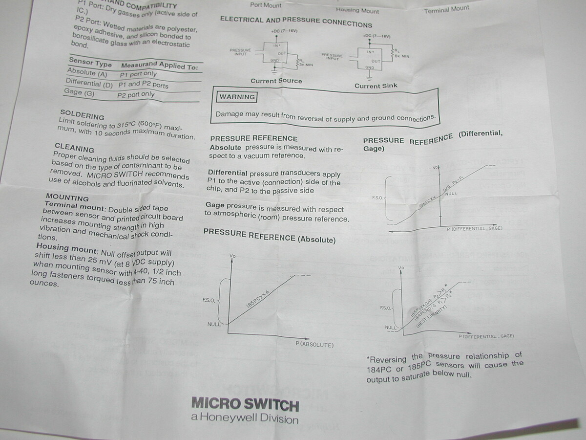
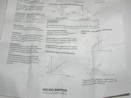
Schaltplan und Diagramme eines Drucksensors
PORT AND COMPATIBILITY P1: Port: Dry gases (only active side of (C.) P2: Port: Wetted materials are polyester, epoxy adhesive, and silicon bonded to a borosilicate glass with an electrostatic bond. ELECTRICAL AND PRESSURE CONNECTIONS PRESSURE INPUT PRESSURE INPUT
in „[VS] verschenke Differential Drucksensor 186PC05DT, +/- 5,0 psi“ · Markt · · Screenshots
-
PDF
Sinuskommutierung_mit_Freilauf_ueber_komp.FET.pdf
Winkelberechnung = 0 SinusU = pM->dV; SinusV = pM->dW; SinusW = pM->dU; CH1 = HallB CH2 = GateB High Side #define UI_PARAM_SENSOR_POLARITY SENSOR_POLARITY_LOW PWM Frequenz = 2kHz, Speed = 300, Verschiebung Winkelberechnung = 0 SinusU = pM->dV; SinusV = pM->dW; SinusW = pM->dU; CH1 = GateB High Side CH2 = GateC High Side #define UI_PARAM_SENSOR_POLARITY SENSOR_POLARITY_LOW
in „BLDC Sinuskommutierung Ansteuerung H-Brücke“ · Analoge Elektronik und Schaltungstechnik ·
-
PDF
BTS55xxGX_SPOC-pb-final.pdf
5590GX SPI Power Controller for Advanced Light Control T H E S P O C products are five channel high-side smart power Basic Features switches in P-DSO-36-20 package providing embedded protective functions. ■ 8 bit serial peripheral interface (daisy chain capable They are especially designed to control standard
in „Defekte Glühbirnen per µC erkennen“ · Analoge Elektronik und Schaltungstechnik ·
-
PDF
EVK2160A_UserGuide.pdf
battery holder on the EVK2160A. Ensure that the battery has the correct orientation (negative (-) side to board) or the EVK2160A will not work. • The 12 LEDs will illuminate in sequence, then extinguish. • Touch and hold the ON/OFF symbol - LED (D11) will illuminate indicating power to the QT2160. Remove
in „CapSense EVK2160A“ · Mikrocontroller und Digitale Elektronik ·
-
PDF
atx2_1.pdf
.....................................................................16 3.4.1 Primary (Component) Side Height Constraints.....................................................................16 3.4.2 Secondary (Bottom/Solder) Side Height Constraints.....................................................
in „Neue PC-Mainboards ohne -5V/-12V lauffaehig?“ · Mikrocontroller und Digitale Elektronik ·
-
PDF
Amp-30W-25-110MHz-BLF244-1.pdf
transformers consist of a twisted-wire-pair transmission line wound on a ferrite toroid. At the input side a special matching network is applied to obtain a low VSWR and compensation for variation in gain with frequency. The matching network at the output side provides the transistors with the optimum load
in „20MHz - 200MHz Isolator bzw. Zirkulator“ · HF, Funk und Felder ·
-
Datei
sensor_three_phase_BLDC.c
/*! \brief Pin Change Interrupt Service Routine. * * Updates the PWM outputs controlling the low side of the driver and * the IO controlling the high side of the driver. To ensure a speed * optimal interrupt the variables used in the interrupt are placed * in reserved registers (locked for this purpose
in „AVR 443 Application: __regvar __no_init unsigned char *pDrvPattern @14;“ · Mikrocontroller und Digitale Elektronik ·
-
PDF
evb2240user.pdf
- 3.1 mil, finished Solder mask Solder Side The component side top layer is shown in Figure 2.2 with silk screen information to identify component locations. Solder side and bottom layer is shown in Figure 2.3. SMSC EVB-USB2240-IND 5 Revision
in „Schaltplan USB2241“ · Mikrocontroller und Digitale Elektronik ·
-
PDF
1331276981-613264.pdf
OB3330 High Performance LED Lighting Driver TheEROB3330CRisTpower factorcorrection, EAPrimary-Side Control with Single Stage PFC advanced features to provide high efficiencyMinimized BOM Count g OB3330 features an internal start-up time fAnalog multiplier for Power Factor Correction power factor
in „LED Netzteil identifizierung“ · Analoge Elektronik und Schaltungstechnik ·
-
 Bild
Bild
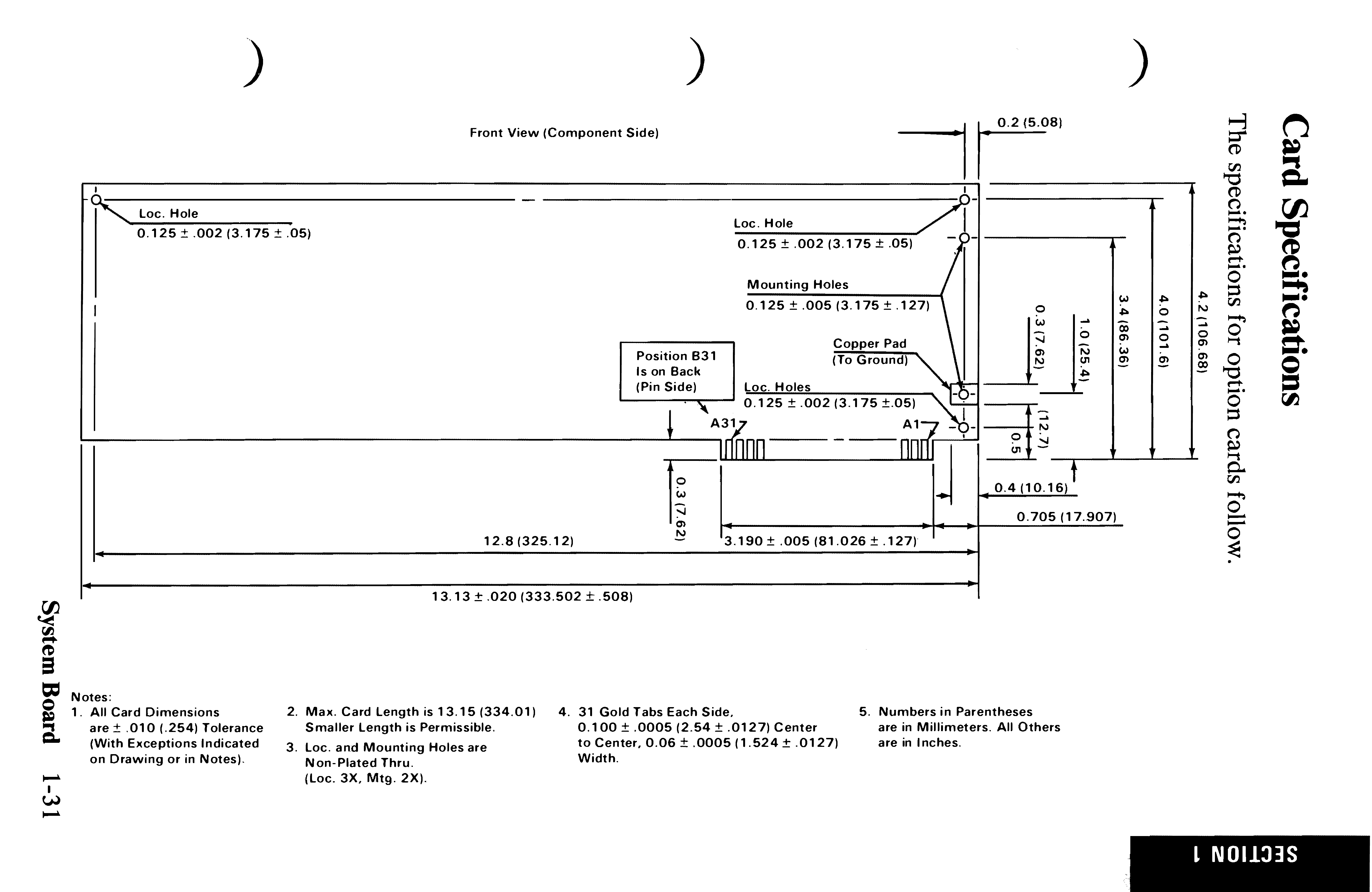
Technische Zeichnung einer Leiterkarte mit Bemaßungen
Front View (Component Side) Loc. Hole 0.125 ± .002 (3.175 ± .05) Loc. Hole 0.125 ± .002 (3.175 ± .05) Mounting Holes 0.125 ± .005 (3.175 ± .127) Copper Pad (To Ground) Position B31 Is on Back (Pin Side) Loc. Holes 0.125 ± .002
in „Suche Datenblatt/Masszeichnung zu ISA Slot“ · Mikrocontroller und Digitale Elektronik · · Screenshots

-
PDF
74LVX4245.pdf
Descriptions E O Pin Names Description t OE Output Enable Input p t T/R Transmit/Receive Input s A0–A7 Side A Inputs or 3-STATE Outputs Connection Diagram B0–B7 Side B Inputs or 3-STATE Outputs Truth Table Inputs Outputs OE T/R L L Bus B Data to Bus A L H Bus A Data to Bus B H X HIGH-Z State H = HIGH Voltage
in „Suche 74LCX04“ · Mikrocontroller und Digitale Elektronik ·
-
PDF
D120591D.pdf
NUMBER FOR THIS STANDARD SPECIFICATION BACKLIGHT MODE L : Bottom Led Backlight (Yellow Green) W : Side Led Backlight (White) S : Side Led Backlight (Yellow Green) Backlight B : Side Led Backlight (Blue) A : Side Led Backlight (Amber) MODULE VERSION SERIES NUMBER FOR THIS STANDARD SPECIFICATION LCD MODE
in „LCD schreibt keine zeichen sonder wechselt die zeile“ · Mikrocontroller und Digitale Elektronik ·
-
PDF
bd7755rfv-e.pdf
Input dead zon(one side) VDZSP1 20 55 90 mV VLRPM=L Input dead zon(one side) VDZSP2 20 240 450 mV VLRPM=H Input output gain H gmSPH 2.68 3.5 4.32 A/V VLRPM=L Spindle Input output gain L gmSPL 0.53 0.7 0.87 A/V VLRPM=H driver
in „Hilfe bei Ansteuerung eines Motortreibers von ROHM (BD7755RFV)“ · Mikrocontroller und Digitale Elektronik ·
-
PDF
IntegratedMagneticsBo.pdf
leakage LLC resonant converter. Two U cores were used to inductance will not only exist on the primary side, it build the resonant inductor and gapped transformer. will also exist on the secondary side of the transformer. Fig.6 shows the simulation results of flux density in the So the result get from real
in „Trafo: Streuinduktivität für LCC Regler berechnen“ · Analoge Elektronik und Schaltungstechnik ·
-
PDF
74lvx4245.pdf
Descriptions E O Pin Names Description t OE Output Enable Input p t T/R Transmit/Receive Input s A0–A7 Side A Inputs or 3-STATE Outputs Connection Diagram B0–B7 Side B Inputs or 3-STATE Outputs Truth Table Inputs Outputs OE T/R L L Bus B Data to Bus A L H Bus A Data to Bus B H X HIGH-Z State H = HIGH Voltage
in „OLED VGY12864Z-S005 über LPT Port ansteuern“ · Mikrocontroller und Digitale Elektronik ·
-
PDF
1683356.pdf
Wash tight: RT III • 2,500 V insulation, input-output input output input output input output Copper side view Copper side view Copper side view Output circuit Contact configuration 1 NO (SPST-NO) 1 NO (SPST-NO) 1 NO (SPST-NO) Rated current/Maximum peak current (10 ms) A 2/20 0.1/0.5 2/40 Rated voltage/
in „Suche RC-Glied für Finder Relais“ · Mikrocontroller und Digitale Elektronik ·
-
PDF
ina169.pdf
INA139 INA169 SBOS181D – DECEMBER 2000 – REVISED NOVEMBER 2005 High-Side Measurement CURRENT SHUNT MONITOR FEATURES DESCRIPTION COMPLETE UNIPOLAR HIGH-SIDE The INA139 and INA169 are high-side, unipolar, current CURRENT MEASUREMENT CIRCUIT shunt monitors. Wide input common-mode
in „Stromaufnahme von Digitaleservo mit ADC messen“ · Mikrocontroller und Digitale Elektronik ·
-
PDF
AV02-3563EN_DS_ACPL-C87x_04Mar2013.pdf
Non-Linearity Max voltagethatisproportionaltotheinputvoltageiscreated • Active-High Shutdown Pin on the other side of the optical isolation barrier. • 100 kHzWide Bandwidth For general applications, the ACPL-C87A (±1% gain • 3V to 5.5VWide Supply Range for Output Side tolerance) and the ACPL-C870 (±3% gain tolerance
in „Hochspannung galvanisch getrennt messen“ · Analoge Elektronik und Schaltungstechnik ·
-
Datei
UTC-Clock_RevC.py
Mainwindow.title("UTC-Clock_RevC.py") Rahmen1 = tk.Frame(Mainwindow, background = "#002040") Rahmen1.pack(side = tk.TOP, fill = tk.X) b = tk.Button(Rahmen1, text = "End", background = "#304000", foreground = "#FFFF5F", command = end) b.pack(side = tk.RIGHT) laMain = tk.Label(Rahmen1, background = "#002040",foreground = "#FFFF5F") laMain.pack(side = tk.LEFT, fill = tk.X) ActualDate() Mainwindow.mainloop()
in „Python 3: Uhr ohne Crash beenden“ · Softwareentwicklung ·
-
PDF
DelSig.pdf
Prototype: void DelSig_Stop (void) Assembly: lcall DelSig_Stop Parameters: None Return Value: None Side Effects: You can modify the A and X registers by this or future implementations of this function. The same is true for all RAM page pointer registers in the Large Memory Model (CY8C29xxx). When necessary
in „Beispiel Anwendungen/Application zu ADCs - Abtastrate & Auflösung“ · Mikrocontroller und Digitale Elektronik ·
-
PDF
3642fc.pdf
Tolerant of 60V Input Transients DC/DCconverterwithinternalhighsideandsynchronous n Internal High Side and Low Side Power Switches power switches that draws only 12μA typical DC sup- n No Compensation Required ply current at no load while maintaining output voltage n 50mA Output Current regulation. n
in „Bauteil LDYM N188 817“ · Analoge Elektronik und Schaltungstechnik ·
-
PDF
MachXO2FamilyDataSheet.pdf
Each MachXO2 device has eight clock inputs (PCLK [T, C] [Banknum]_[2..0]) – three pins on the left side, two pins each on the bottom and top sides and one pin on the right side. These clock inputs drive the clock nets. These eight inputs can be differential or single-ended and may be used as general purpose
in „Statemachine springt in falsche "states" warum?“ · FPGA, VHDL & Co. ·
-
 Bild
Bild
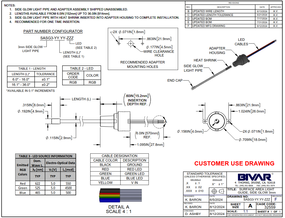
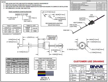
Technische Zeichnung einer LED-Leuchtleitung
NOTES: 1. SIDE GLOW LIGHT PIPE AND ADAPTER ASSEMBLY SHIPPED UNASSEMBLED. 2. LENGTHS AVAILABLE FROM 6.0IN [152mm] UP TO 36.0IN [914mm]. 3. SIDE GLOW LIGHT PIPE WITH HEAT SHRINK INSERTED INTO ADAPTER HOUSING TO COMPLETE
in „Bauteil-Roundup: Drohnenkit bis Piezoputzanlage“ · Mikrocontroller und Digitale Elektronik · · Screenshots
-
PDF
VisiLogic_-_Communications.pdf
Wait for Places the PC modem in auto-answer mode. Incoming Call Use this option to initialize a PLC-side modem. Full instructions are in the topic Prepare PLC Modem PLC-side Modems. How to use the PC modem to access a PLC 1. Prepare and connect the PLC-side modem as described in the topic PLC- side Modems
in „USB-Host / industrielle SPS / Frequency Counter“ · Mikrocontroller und Digitale Elektronik ·
-
PDF
L6207_AN.pdf
includes logic for CMOS/TTL interface, a charge pump that provide auxiliary voltage to drive the high-side DMOS, non dissipative over current protection circuitry on the high-side DMOS, with fixed trip point set at 5.6 A (see Over Current Protection Section), over temperature protection, Under Voltage Lock
in „Schrittmotor mit L6207“ · Mikrocontroller und Digitale Elektronik ·
-
PDF
en.CD00004482.pdf
includes logic for CMOS/TTL interface, a charge pump that provide auxiliary voltage to drive the high-side DMOS, non dissipative over current protection circuitry on the high-side DMOS, with fixed trip point set at 5.6 A (see Over Current Protection Section), over temperature protection, Under Voltage Lock
in „Treiberstufe fuer Faulhaber Schrittmotor“ · Mikrocontroller und Digitale Elektronik ·
-
PDF
TEA5880_2.pdf
point at LNA input IP3 out-band 3rd order - 95 - V dB out intercept point at LNA input S −300 LOW side 300 kHz f = −300 kHz; RF= 76 MHz to 108 MHz - 40 - dB selectivity S +300 HIGH side 300 kHz f = 300 kHz; RF= 76 MHz to 108 MHz - 50 - dB selectivity S −200 LOW side 200 kHz f = −200 kHz; RF= 76 MHz to
in „Einfaches Radio basteln“ · Mikrocontroller und Digitale Elektronik ·
-
PDF
LQ043T3DX02_SP_122805.pdf
No.: FH12A-40S-0.5SH(55) Top contact type) 㶎 The Bottom contact type can be selected according to side of mounted connector and terminal side of FPC. Terminal No. Terminal name Function Remarks 1 GND GND(0V) 2 GND GND(0V) 3 VCC +2.5V power source 4 VCC +2.5V power source 5 R0 RED Data Signal (LSB) 6
in „Ansteuerung PSP Display möglich??“ · Mikrocontroller und Digitale Elektronik ·
-
PDF
LQ043T3DX02.pdf
No.: FH12A-40S-0.5SH(55) Top contact type) 㶎 The Bottom contact type can be selected according to side of mounted connector and terminal side of FPC. Terminal No. Terminal name Function Remarks 1 GND GND(0V) 2 GND GND(0V) 3 VCC +2.5V power source 4 VCC +2.5V power source 5 R0 RED Data Signal (LSB) 6
in „Suche Display für NGW100“ · Mikrocontroller und Digitale Elektronik ·
-
PDF
TCA9406_I2C_translator.pdf
level configuration of the I C-bus. The value of pullup resistors depends on the system, but each side of the translator must have pull-up resistors and TCA9406 already has 10 kΩ pullup resistors on each side and it allows to add additional external pull-up resistors. It can work with 2 standard-mode
in „I2C translator tri-state“ · Mikrocontroller und Digitale Elektronik ·
-
Datei
nomo.py
': 0.5, 'tick_levels': 3, 'tick_text_levels': 1, 'tick_side': 'right', 'text_format': '%.0f' } scale3 = { 'u_min': 5 / 3, 'u_max': 15, 'function_x': lambda u: 1, 'function_y': lambda u: (u - 5 / 3) / (15 - 5 / 3), 'title': r'$\rm l/s$', 'title_x_shift': 1.2, 'title_y_shift': 0.5, 'tick_levels': 3, 'tick_text_levels': 1, 'tick_side': 'right', 'text_format': '%.0f' } block1 = { 'block_type': 'type_8', 'f_params': scale1 } block2 = { 'block_type': 'type_8', 'f_params': scale2 } block3 = { 'block_type': 'type_8', 'f_params': scale3
-
PDF
WG320240BX-TFHVZ_021__1.pdf
T.P) 19 FG 0 4-O6.0PAD . 1.0 5 2 (PCB) 20 WAIT . 1 Supporting tape 2 37.9 LED B/L 0.3±0.05 (contact side as PCB DETAIL A component's side) SCALE 2/1 0.36 1 Right O1.1mm,UL1007(30AWG) 0.34 2 Left 5.0±1 5.0±1 . 3 Bottom 0 8 4 4 Top 3 3 50.0±5.0 0 0DOT SIZE 0.7 Note: SCALE 10/1 1.0 P1.0*19=19 The stiffen tape of the FFC cable is in the same diraction 21.0 as LCD panel side.and it's contact side as PCB component's side 6 200.0±5.0 Page 1 of 25 CL1 RD M r o WR FLM v ~ A0 r 0 DB0~DB7 S1D13700 CS RES SEL1 * Controller D m v ~ r 0 320X240 DOT MPU C D m N v 1 Vdd i r t r 4
in „[V] 8 LCDs 320x240 s/w, 6 Zoll, Touch, inkl Controller“ · Markt ·
-
PDF
WG320240BX-TFHVZ_021__1.pdf
T.P) 19 FG 0 4-O6.0PAD . 1.0 5 2 (PCB) 20 WAIT . 1 Supporting tape 2 37.9 LED B/L 0.3±0.05 (contact side as PCB DETAIL A component's side) SCALE 2/1 0.36 1 Right O1.1mm,UL1007(30AWG) 0.34 2 Left 5.0±1 5.0±1 . 3 Bottom 0 8 4 4 Top 3 3 50.0±5.0 0 0DOT SIZE 0.7 Note: SCALE 10/1 1.0 P1.0*19=19 The stiffen tape of the FFC cable is in the same diraction 21.0 as LCD panel side.and it's contact side as PCB component's side 6 200.0±5.0 Page 1 of 25 CL1 RD M r o WR FLM v ~ A0 r 0 DB0~DB7 S1D13700 CS RES SEL1 * Controller D m v ~ r 0 320X240 DOT MPU C D m N v 1 Vdd i r t r 4
in „[v] LCDs 320x240 s/w, 6 Zoll, Touch, inkl Controller“ · Markt ·
-
PDF
WG320240BX-TFHVZ_021__1_320-240_display.pdf
T.P) 19 FG 0 4-O6.0PAD . 1.0 5 2 (PCB) 20 WAIT . 1 Supporting tape 2 37.9 LED B/L 0.3±0.05 (contact side as PCB DETAIL A component's side) SCALE 2/1 0.36 1 Right O1.1mm,UL1007(30AWG) 0.34 2 Left 5.0±1 5.0±1 . 3 Bottom 0 8 4 4 Top 3 3 50.0±5.0 0 0DOT SIZE 0.7 Note: SCALE 10/1 1.0 P1.0*19=19 The stiffen tape of the FFC cable is in the same diraction 21.0 as LCD panel side.and it's contact side as PCB component's side 6 200.0±5.0 Page 1 of 25 CL1 RD M r o WR FLM v ~ A0 r 0 DB0~DB7 S1D13700 CS RES SEL1 * Controller D m v ~ r 0 320X240 DOT MPU C D m N v 1 Vdd i r t r 4
in „Anstuerung eines Grafik LCDs. Fragen zu Display und Controller“ · Mikrocontroller und Digitale Elektronik ·
-
PDF
2003092109_PTC-Princeton-Tech-PT4308_C481966.pdf
double-balanced mixers that perform an I-Q down-conversion of the RF input to the IF band with high-side injection (i.e. fRF = LO –fI). The image-rejection circuit then combines these signals to achieve an image-rejection ratio typically over 25 dB. High-side injection is mandatory (e.g. low-side injection
in „Superheterodynempfänger oder was?“ · HF, Funk und Felder ·
-
PDF
7212-910.pdf
adjusted to be centered in the air gap for that specific mounting plane. Simplified cross-sectional side view of a reverb tank: Horizontal Open Side Down mounting plane. Gravitational pull on the transmission springs displaces the OPEN SIDE magnets toward the lamination. Mechanical Isolation: 6 The reverb
in „Driver für Reverb Tank 9AB3C1B“ · Analoge Elektronik und Schaltungstechnik ·
-
 Bild
Bild
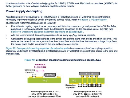
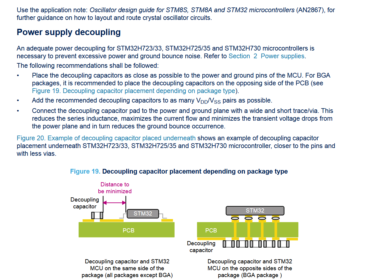
Anleitung zur Entkopplung der Stromversorgung bei STM32 Mikrocontrollern
of the MCU. For BGA packages, it is recommended to place the decoupling capacitors on the opposing side of the PCB (see Figure 19. Decoupling capacitor placement depending on package type). • Add the recommended decoupling capacitors to as many VDD/VSS pairs as possible. • Connect the decoupling capacitor
in „Abblockkondensatoren die 99te“ · Platinen · · Screenshots