pins logic high. The corresponding INHx and INLx signals control the output state as listed in Table 8-2. Table 8-2. 3x PWM Mode Truth Table INLx INHx GLx GHx SHx 0 X L L Hi-Z 1 0 H L L 1 1 L H H 8.3.1.1.3 1x PWM Mode (PWM_MODE = 10b or MODE Pin = Hi-Z) In this mode, the DRV835xF family of devices uses
, 8-pad WSON 6x5 & 8x6-mm (Package Code P & E) 3.2 Pad Description WSON 6x5-mm/ 8x6-mm PAD NO. PAD NAME I/O FUNCTION 1 /CS I Chip Select Input 2 DO (IO1) I/O Data Output (Data Input Output 1) (2) 3 /WP (
15 ~ 20 13. INSPECTION CRITERION -------------------------------------------1 ~ 30 02101300-01-02 E M E R G I N G D I S P L A Y MODEL NO. VERSION PAGE TECHNOLOGIES CORPORATION E T 0 3 5 0 G 0 D H 6 7 1 1. GENERAL SPECIFICATIONS 1 . 1 APPLICATION NOTES FOR CONTROLLER/DRIVER PLEASE REFER TO : H X 8 2
gn/ge F bl gr D C br P sw T 1 0 VD-14N,VD-15 gn/ge F bl gr D br C P T sw 1 a b 6 Coldmachine c 1 2 3 d A B C D 7 Coldmachine e 1. 2. f g 2mm 21 19 21 16 3mm h Ø/mm² 12V 24V 14 10 6 2 0 l/m 0 2 4 6 8 10 12 14 16 18 20 22 24 26 28 8 Coldmachine i VD-01,VD-02,VD-03,VD- 04,VD- 05, VD-07,VD- 08,VD- 09,VD
— 13 September 2021 4 / 41 Nexperia AN50005 Paralleling power MOSFETs in high power applications P E diss diss (W) (µJ) 110 I 55 ID M1 11 D (A)45 90 9 M1 35 E SW(on) E diss 70 7 5 25 50 P dissM1 15 30 3 P COND 10 5 1 -10 -1 -5 9.6 10 10.4 10.8 11.2 time (µs) aaa-033730 Fig. 3. MOSFETs drain current
Maschinen mit weniger als 16GB RAM. Keine Probleme soweit. In diesem Moment auf ’nem ältlichen T440 mit 8GB RAM und ohne Swap, mit FF mit einer Handvoll Tabs, dazu VSCode und Logseq als fully bloated Electron „Apps“. X. H. schrieb im Beitrag #7483476: > Dann geht nur noch S-Abf mit REISUB. Geschickter
fonctionner depuis un périphérique iOS capable d’exécuter iOS 4.2 ou une version ultérieure (iPhone 3 G, 3GS , 4 Dimensions HxLxP : 195 x 310 x 185 mm ou 4S, iPod touch 2e, 3e ou 4e génération, iPad, iPad 2 ou iPad 3). Entrées : AirPlay (et DLNA ), stéréo 3,5 mm, US B, TOSL ink optique Sortie : caisson
7.5.1 Relationship between f and µ p These curves show the relationship between f and µ, to be :p x fp= K / [µ ] fHz 7.5.1 where K= 5300 and x = 1.16 (for Fair-rite materials) Substituting this equation into the second term of Equation 7.3.1, and noting that A = µ µ A / l = 0.4 π L o f e e 3 2 2 10 µ A f l ehere A is in µH/NL, and A is in mm and l inemm. e 10 /[(2π k f ) p N ] L 10 µ 9 f(2x-1)le/ [(2π k) K 0.4π A N ] e 2 9 (2x-1) 2 2 2 =10 µ f le/ [ 49.6 k K A N ] e Equation 7.3.1 then becomes : -3 2 9 (2x-1) 2 2 2 C’ self≈ [1.13 10 l l e p ] / [0.4 π
. 3 Payne : Self Resonance in Coils Coil Q 1.2 1.0 0.8 Q o 0.6 Coil Q C 0.4 0.2 0.0 0.00 0.20 0.40 0.60 0.80 1.00 Frequency Norm alised to SRF Figure 3.1 Coil Q with the effects of SRF It is important therefore
= 2πf v p i.e., since the reactance is inductive: R 0 w X L 2πf 2v p This has the same form as the lumped-element formula for inductive reactance; i.e., we find that: R 0 w L= 2v (1.3) p Unfortunately, we must be
0.45 0.55 c L1 0.60 REF. e e 0.95 BSC. b2 e1 1.90 BSC. θ 0 5 10 θ1 3 5 7 6 8 10 θ1 θ2 2 A A GAUGE PLANE SEATING PLANE 1 θ A L θ2 L1 DETAIL A Dimension (Package B) D e1 DETAIL A Unit : mm b SYMBOL MIN. TYP. MAX. A 1.050 - 1.250 A1 0.000 - 0.100 A2 1.050 - 1.150 b 0.300 - 0.400 c 0.100 - 0.200 1 E D 2.820 - 3.020 E E 1.500 - 1.700 E1 2.650 - 2.950 e 0.950 TYP e1 1.800 - 2.000 c L 0.700REF e L1 0.300 - 0.600 θ 0 - 8 2 A A GAUGE PLANE 0.2 SEATING PLANE 1 θ A L1 L DETAIL A Fortune Semiconductor Corp
D U T T T T T S L D / / / / / D / / / / / D S 3 2 1 D 0 9 8 7 6 5 4/ D 3 S 2 D 1 0 9 8 7 6 5 4/ O Y _ G O R A V V O P A O V O A O V O E E E E E V C D 6 6 6 6 5 D 5 5 5 5 5 D V 5 5 5 D 5 4 4 4 4 4 4 D 4 V 4 D 4 4 3 3 3 3 3 3 M D S X C V A A O C A A
.) mm (WITHOUT FPC) → g 166W * 105.44H *9.8dD(MAX.) mm (WITHOUT FPC & LED BL’S CABLE) 9 n 7. MARK △E DIM2NS: MODIFY PCB & CHANGE C/N TYPE, ADD BOTTOM FRAME SEP.30, 2009 3 g i 4. ELECTRICAL CnARACTERISTICS e r VDD-VSS o 3.0(MIN.) → 3.2(MIN.) DEC
0 d B , th e fo llo w in g v o lta g e is o u tp u t: V 1 (-1 O ) = (3 /3 .1 6 x 1 /0 .6 2 R + 9 x 3 /R ) x R 1 3 = 9 .4 9 '/ S im ila r ly , 1 1 v1 (-2 0 ) = ( 10 x 0 6 2 + 3.16 + 8 ) V = 8 .4 7 V V1 (-3 0 ) = 1
of the inverter is not included.) PRELIMINARY DATA SHEET DOD-PD-1288 (2nd edition) 5 NL6448BC33-63D 3. BLOCK DIAGRAM Host LCD module (Product) D0+ 100 H-driver D0- D1+ 100 S V D1- L D2+ f 1,920 lines e 100 i c D2- r D3+ i w LCD panel 100 e s r r i n v 0 H: 640 × 3 (R, G, B) D3- C d 4 V: 480 CK+ V 100
A4915 Demo Board Schematic/Layout D C B A SCHEMATIC C 2 V v r T C N C l m o N D 7 6 5 4 3 2 1 0 O g v s 3 4 3 2 1 e e a J o M o M e 1P i 1 V a v D d t 1 t o g 1 H t n o A R R R p ce h 1 1 1 n ther D C 9 8 1 6 . e a D H 7 C p n B 2 l V L k k k k y , D 1 1 u F k R 4 R 5 . 4 k U B N 2 N G G
= 0; uint8_t file_tring[10]; #endif // Stepper ISR data struct. Contains the running data for the main stepper ISR. typedef struct { // Used by the bresenham line algorithm uint32_t counter_x; // Counter variables
established, if the connection has established, and you can test the data transport transmission. 3.More information reference the below: http://www.usr.cn/Search/getList/keyword/%E8%99%9A%E6%8B%9F%E4%B8%B2%E5%8F%A3/ 4.3. Serial Port Function Jinan USR IOT Technology Limited 37 / 107 inquiry@usriot.com
160 10,000 5 F 2 140 P6SMB6.8AT3G O =A ) % T 120 p1000 I T ( P6SMB18AT3G I E 100 C A R N R U 80 T P6SMB51AT3G D C C 100 S O A U R 60 A P W C A O 40 C 10 P6SMB200AT3G P K TJ= 25°C E 20 f = 1 MHz P 0 1 0 25 50 75 100 125 150 1 10 100
NORWAY Date: 07.06.2011 15:02:09 PAGE: 6 of 7 Document number: 6 Revision: 2 TITLE: Memory XMEGA-A3BU_XPLAINED_Memory.SchDoc 1 2 3 4 5 6 7 8 1 2 3 4 5 6 7 8 A A NHD-C12832A1Z-FSW-FBW-3V3 LCD500 Backlight: I = 30mA @ 3.0V resistor is needed.onsumption at 3.3V a 128x32 The FET has max RDSon = 5Ohm Limiting resistor 10 Ohms Backlight current: B ) Imin = 0.3V /(15 Ohm) = 20 mA B S E 0 1 2 3 4 2 2 1 1 O S D D C 0 S E L V V V V V C C C C V V V S S A R L A 1 2 3 4 5 6 7 8 0 1 2 3 4 5 6 7 K VCC_P3V3 5A P1 2 3 46 7 89112 1 3 461 171 5K CR00 I0 10R I0 2 3 2N7002
Rudi schrieb im Beitrag #7462017: > @Christian M > Die Betriebsspannung kann bis 1,8V abfallen. Wir reden doch vom originalen Raspberry Pi Pico mit diesem Winbond Speicher? Laut Datenblatt braucht der W25Q16JV 3.3V ±10% zum Schreiben; Lesen geht auch noch mit 2.7V. Aber man kann
originalen Raspberry Pi Pico mit diesem Winbond > Speicher? Laut Datenblatt braucht der W25Q16JV 3.3V ±10% zum Schreiben; > Lesen geht auch noch mit 2.7V. Auf dem Pi Pico ist ein RT6150A/B verbaut, der arbeitet von 1.8V an aufwärts und erzeugt die 3.3V für das System.
3 mm x 3 mm x 1 mm QFN Document Number: DS-000189 Page 19 of 89 Revision: 1.3 ICM-20948 4.2 TYPICAL OPERATING CIRCUIT VDDIO nCS SCL SCLK K K SDA I L SDI I L S S A S S A / L _ V V / L _ V V D C C U E E
Frequency vs Temperature - "X" Figure 4. Oscillator Frequency vs Temperature - "Y" 93.4 96.55 96.5 93.3 96.45 ) 93.2 E ( L 96.4 L Y Y 93.1 C 96.35 Y T 96.3 U U D 93.0 D 96.25 A A M 92.9 M 96.2 96.15 92.8 96.1 92.7 96.05 -40 -25 0
Projektion ist, was dann? Bravo! https://www.amazon.de/-/en/Hans-Hofmann-Reinecke/dp/B096XKSZNH/ref=sr_1_3?crid=1O35Q1LSP6H1X&keywords=gr%C3%BCn+und+dumm&qid=1689764935&sprefix=gr%C3%BCn+und+dumm%2Caps%2C90&sr=8-3
1Q 2 19 8D OE CLK D Q 1D 3 18 8Q L H H 2Q 4 17 7D L L L L L X Q 0 2D 5 16 7Q H X X Z 3Q 6 15 6D 3D 7 14 6Q OE 1 4Q 8 13 5D CLK11 C1 2 4D 9 12 5Q 1D3 1D 1Q GND 10 11 CLK 15. SN74LVC1G08 (IC43) 1A 1 14 VCC 1B 2
EMI interference, as the frequency emissionsofthecircuitwillbemuchmorepredictable BV CES 800~1kV 1.3~1.5kV 1.6kV andtestable. 8/10 APPLICATION NOTE 4.3Currentratings Thecalculationofthecurrentratingofthetransistors usedvariesconsiderablydependingonthetopology, powerratingetc.Table1showsapproximate values
(33dBm±2dB) for GSM900 Class 1 (30dBm±2dB) for DCS1800 Class 1 (30dBm±2dB) for PCS1900 Class E2 (27dBm±3dB) for GSM850 8-PSK Class E2 (27dBm±3dB) for GSM900 8-PSK Class E2 (26dBm±3dB) for DCS1800 8-PSK Class E2 (26dBm±3dB) for PCS1900 8-PSK Class 3 (24dBm±1dB) for CDMABC0 Class 3 (23dBm
Kingbright PSC Serie (16 Segment LED-Display, insbesondere PSC08 und PSC12) | LED Punktmatrix Anzeigen 8x8 superrot 3mm (z. B. Everlight ELM-1883SRWA) * LED Punktmatrix bicolor 1.9mm (z.b. Betlux BL-M 07A881SG-XX ) LED Punktmatrix (Dot-Matrix) 8x8 RGB (z.B. Betlux BL-M 23B881RGB-11) | TFT/OLED Farb-Displays
und ICs. Buchsenleiste vergoldet, 2,54, 8mm, Einreihig, t r e n n b a r | Buchsenleiste vergoldet, 2,54, 8,5mm, Einreihig, trenn,- und druchsteckbar | Buchsenleiste Fischer BL5 | Buchsenleisten zum Crimpen (allseitig anreihbar!, 1x1, 1x2, z.
durch die mAh-Angabe des Datenblattes dividiert, kommt man auf eine mittlere Spannung von 1,1487V: @R=3,9 Ohm: Energy [mWh] 2826 Capacity [mAh] 2460
questions/571226/how-many-amperes-can-an-alkaline-aa-battery-supply Energizer datasheet shows the same trend, at 500mA the capacity is reduced to 1500mAh, where it does 3000mAh at 25mA. https://data.energizer.com/pdfs/e91.pdf
= 10 kHz A E ( C 8 E = 0 A T 10 TA= −25°C N 7 TA= 25°C E I R C 6 R P C 1 A 5 R C O U 4 T P E 0.1 U 3 L O O b 2 ,0.01 C 1 I VO= 5 V 0 0.001 0 10 20 30 40 50 0 1 2 3 4 5 6 7 8 9 10 V , REVERSE VOLTAGE (V) V , INPUT
Ich bin dabei die Konfiguration für die Clock Chain eines AtSamC21E15A einzustellen. Dabei bin ich darüber gestolpert, dass laut Datenblatt für das FDPLL96M Modul als Quelle der Generic Clock Controller möglich ist. Der Generic Clock Controller hat ja 8 Generatoren
Dann lass das #include "sam.h" auch noch weg. Olivr
F. K. schrieb im Beitrag #7447075: > Jetzt sind aber immer noch 1,3kB vom Ram belegt Mir ist da die Zeile aufgefallen: [pre] .data.impure_data 0x20000008 0x428 c:/ ... libc.a(lib_a-impure.o) [/pre] Und ich habe damit den https://www.mikrocontroller.net
definitions have been moved from the 'spi_flash' to the new component 'esp_partition'. See Storage 5.x migration guide for more details (b14116f) • esp_chip_info() returns the chip version in the format = 100 * major eFuse version + minor eFuse version. (c546de8) • Wi-Fi: Modified maximum
Fix the iPhone disconnects immediately after connecting when BLE and wifi coexist on ESP32-C3 and ESP32-S3 (e8dba71) [/c] ### Ausblick und Mehr Espressif bietet unter der URL https://docs.espressif.com/projects/esp-idf/en/latest/esp32/migration-guides/release-5.x/5.1/index.html umfangreiche
wie SoyoSource GTN1200 recht einfach, legale WR mit denen das geht sind deutlich teurer. Viktor E. schrieb im Beitrag #7443834: > Wenn man da jetzt noch etwas mit Notstrom noch basteln könnte, wäre das > für mich eine optimale Lösung Kostet halt das doppelte bis 3-fache und macht nicht nur
einer Insel > leben würde. Da sind dann die Kosten zweitrangig. https://de.wikipedia.org/wiki/Sams%C3%B8#Wirtschaft
products/uno-r4-wifi wechselt die größere Variante um 25 EUR den Besitzer. Neben einem auf einem ESP32-S3 basierenden Funkmodul bringt sie eine LED-Matrix (12x8 rote LEDs) mit. 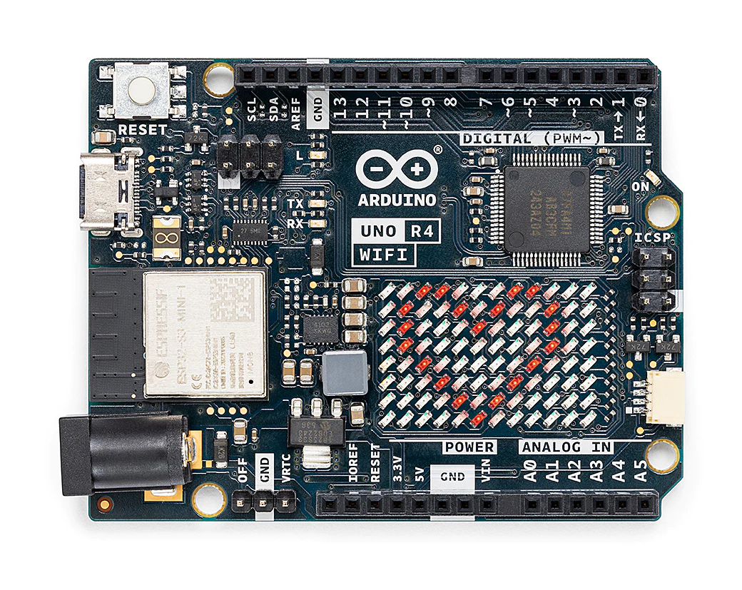 Bildquelle: Arduino Bei sorgfältiger Betrachtung fällt ein QWIIC-Interface auf, das einen
könnte man sich so etwas mit den etwas einfacheren Varianten der RISC-V-µCs von WCH bauen, der CH32V103x8x6 wäre da ein Kandidat. Kann mit 5V betrieben werden (also nicht nur 5V-tolerante I/Os), 20 kiB RAM, 64 kiB Flash, bis zu 72 MHz CPU-Takt, LQFP/QFN48 und LQFP64. Ist wohl was die Peripherie angeht,
51 0x1d Character 3 2 32 0x1e Character 4 0 30 0x1f Character 5 8 38 0x20 Character 6 3 33 0x21 Character 7 — 00 0x22 Device Chemistry Length 4 04 0x23 Character 1 L 4c 0x24 Character 2 I 49 0x25 Character
carrier offset frequency in Hz m QL(=pF t0 g= loaded Q of the resonator in the feedback loop aRand a E flicker noise constants for the resonator and loop amplifier, respectively More detailed information about this is given in the original paper by Leeson and in [3]. The following table shows the flicker
= 1.5V or 13.5V 11.0 11.0 8.25 11.0 V IOL LOW Level Output Current VDD = 5V, O = 0.4V 0.52 0.44 0.88 0.36 mA (Note 4) VDD = 10V, O = 0.5V 1.3 1.1 2.25 0.9 mA VDD = 15V, O = 1.5V 3.6 3.0 8.8 2.4 mA IOH HIGH Level Output Current
