einer unheimlich vertrauten Stimme. Der Operator erkannte die Stimme sofort, es war die Stimme des T-800 aus dem Film Terminator 2. Der Baukran hatte sich in einen Terminator verwandelt. Der Operator starrte den Baukran an, der die Dose Milch mit Leichtigkeit hoch und runter bewegte. "Hasta la vista
Terminator-Baukran, der nun die Kontrolle über den Bauplatz hatte. Der Operator dachte daran, wie der T-800 im Film gesagt hatte: "The future is not set. There is no fate but what we make for ourselves". Er wusste, dass sie sich zusammenschließen mussten, um diesen Terminator zu besiegen. Die Arbeiter
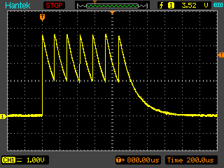
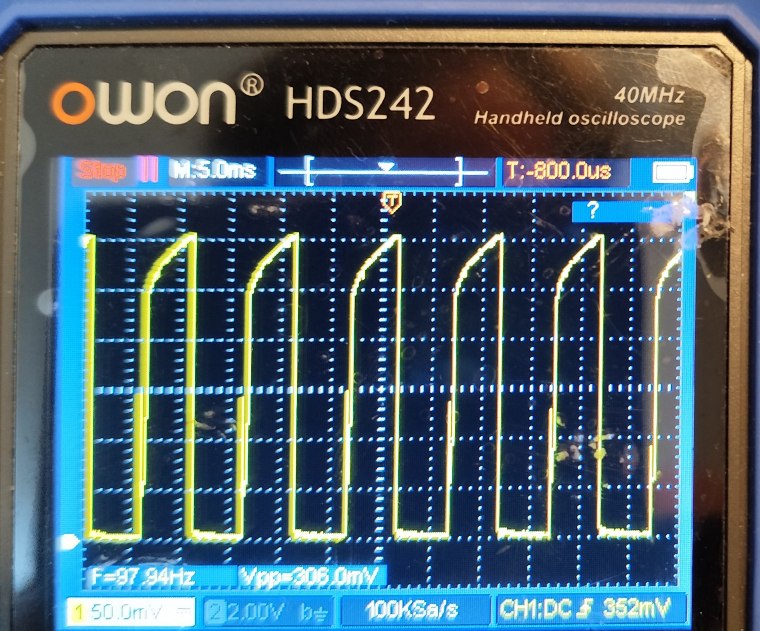
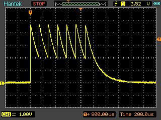
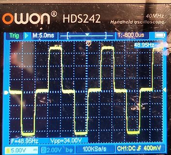
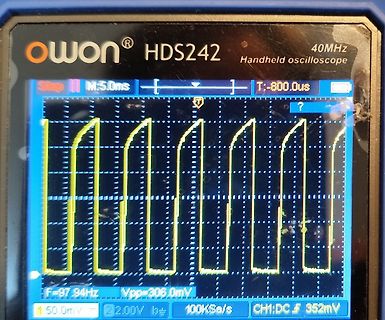
Umrichter_an_Master_Start.jpg" sieht man den Übergang vom passiven Bus zum Senden einer Nachricht des Masters (bei ca. t=800ms). In "RS485_Umrichter_an_Detail.jpg" ein zufälliger Ausschnitt eines Frames, wenn die Anlage läuft. Insgesamt sind die Timings beim Umschalten zwischen Senden und Empfangen in Ordnung und die
Occam es auf den T2xx/T4xx nicht benötigte. Bei einer Umsetzung von C war das recht nervig. Erst beim T800 mit FPU wurde DUP eben dafür erforderlich und folglich implementiert.
kommen dann diesselben Fragen auf wie beim > selbstfahrenden Auto. Achwas! Ich würde gleich den T800 bauen, satte 200kg Titan, Carbonfaser, Atombatterien und ein 6502! Was soll schon schief gehen? Ähmm, einen Moment Frau Connor, ich bin gleich für Sie da . . . ;-)
brachte z.B. den BCM384y120x800AC0 zu Tage: http://www.vicorpower.com/documents/datasheets/ds_BCM384P120T800AC0.pdf 800W auf kleinstem Bauraum (61 x 25.14 x 7.26mm), Vin 260 - 410V DC, Vout 12V. Natürlich nur als erster Schritt, eine gründliche Einarbeitung, Filter, Schutzbeschaltung... fehlen.
Überlegung ist nun, dafür eine Drahtbrücke mit einer richtigen Sicherung zu ersetzen. Der erste Versuch (T800ma) war (wie zu erwarten) zu klein dimensioniert und ist beim Schleudern durchgebrannt. Aktuell sind T4A drin und die Sicherung hat einmal leer bei voller Drehzahl Schleudern überlebt. Was würdet
muss schickt man dem nen Satz Daten über den SPI für Kommandos: [code] ft800_cmd_dl(TAG(12)); t800_cmd_button(150, 100, 100, 20, 26, button, "Click"); [/code] Das sind 3 Bytes Adresse, plus 16 Bytes Kommando plus 8 Bytes für den Text (muss durch vier teilbar sein) -> 27 SPI Transfers für das
waren die AD2200, die PACE 90 Station und Hakko FX888. Als schlechteste schnitt ein Chinesischer T800 Klon ab. Das lag aber hauptsächlich an den losen Toleranzen zwischen Keramikheizkörper und den fehlenden Kupfermantel echter Hakko-Spitzen. Eine WT1010 schnitt im Zeitverhalten auch etwas schlecht ab
Pulse/Surge Chart @ 50 msec duration 700 1400 1400 600 1200 1200 s s s p 500 p1000 p1000 A A A t 400 t 800 t 800 e e e u u u C 300 C 600 C 600 g g g u 200 u 400 u 400 S S S 100 200 200 0 0 0 0 10 20 30 40 50 60 70 80 90 100 0 10 20 30 40 50 60 70 80 90 100 0 5 10 15 20 25 30 35 40 45 50 Resistance (milli-ohms
t800w schrieb im Beitrag #4959059: > Doch wenn ich diesen Code zum Schieberegister schicke, werden alle LEDs > auf HIGH gesetzt, woran liegt das? [c] pinMode(speicherPin, OUTPUT); pinMode(taktPin
gigantischer Durchbruch zur Speicherung elektrischer Energie gelingt - wie beispielsweise die Batterie eines T-800, dann wird das eine verdammt schwere Sache. Ich glaube eher, daß kein heute lebender Mensch auf der Erde praktisch einsetzbare elektrische Großflugzeuge erleben wird.
Current 1200 1200 1200 1000 1000 1000 R = 50Ω A R = 30Ω A R = 36Ω A L ( L ( IL= 50mA* ( IL= 50mA* T800 IL= 50mA* T800 L T800 E TJ= 25°C E TJ= 25°C E TJ= 25°C R VIN= VSHDN R VIN= VSHDN R VIN= VSHDN C600 *FOR VOUT = 1.5V C600 *FOR VOUT = 1.8V C600 *FOR VOUT = 2.5V N N N P P P D400 RL= 150Ω D400 RL= 180Ω
nicht rechtzeitig liefern konnte. Hah, so ein Teil stand bei uns an der Uni auch (16x (oder 64x?) T800). Nur Occam haben wir darauf nicht betrieben, einfach C unter Helios OS...
Current Figure 12B. Offset Supply Leakage vs. Temperature Current vs. V Boost Voltage 1000 1000 ) ) t 800 ( 800 n n r 600 r 600 C u l y p 400 p 400 u M ax. u S 200 S M ax. V 200 Typ. V Typ. 0 0 -50 -25 0 25 50 75 100 125 10 12 14 16 18 20 Temperature () VBSSupply Voltage (V) Figure 13A. V Supply Current
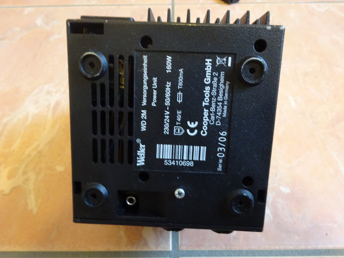
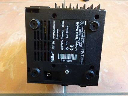
Weller WD 2M Versorgungseinheit Power Unit 230/24V - 50/60Hz 160W T800mA CE Cooper Tools GmbH Carl-Benz-Straße 2 D-74354 Bergheim Made in Germany Ser. nr.: 03/06 53410698
Lineare Rampe S-Förmige Rampe 1000 3500 1200 3500 900 3000 e 800 c 1000 3000 / / p 700 2500 s 2500 t t 800 s 600 2000 s t t i 2000 e e 500 r e 600 r g 400 1500 c k 1500 c d S d S i 300 1000 i 400 h w 1000 s 200 c e 500 e 200 500 G 100 G 0 0 0 0 0 1 2 3 4 5 6 7 0 1 2 3 4 5 6 Zeit in sec Zeit in sec Geschw
] Lineare Rampe S-Förmige Rampe 1000 3000 1200 3000 900 e 800 2500 c 1000 2500 / / p 700 s t 2000 t 800 2000 s 600 s t t i e e 500 1500 r e 600 1500 r g 400 c k c d S d S i 300 1000 i 400 1000 h w s 200 500 c e e 200 500 G 100 G 0 0 0 0 0 1 2 3 4 5 6 7 0 1 2 3 4 5 6 Zeit in sec Zeit in sec Geschw indigkeit
VBS Supply Current Figure 8A. VBS Supply Current vs. Temperature vs. Temperature A 1000 )1000 ( ( t 800 t 800 e e u 600 u 600 C C l 400 Max. l 400 p p Max. u u SC 200 Typ. C 200 VC C Typ. 0 V 0 -50 -25 0 25 50 75 100 125 10 12 14 16 18 20 Temperature () V Supply Voltage (V) BIAS Figure 9A. Vcc Supply
für eine 50/60 Hz Sinus-Halbwelle 2 2 Rating for fusing, Grenzlastintegral, t < 10 ms TA= 25°C i t 800 A s Junction temperature – Sperrschichttemperatur T j -50...+175°C Storage temperature – Lagerungstemperatur TS -50...+175°C 1 Valid, if leads are kept at ambient temperature at a distance of 10 mm
switch resistive or inductive loads T to 0.2 power factor. The dv/dt rating is based on a source E T 800 impedance of 50 ohms. R E U R 2. For any mounting conditions: 5-amp relays,JA = 19°C/W. C U 600 For 10-amp relays, θJS 4.8°C/W. G C 3. Basic part number provides screw terminals or PC board R E 400
1 1400 t o 14 o 0 / / T A +25 ° / 1200 6 1.0 6 12 6 7 M ) A A V1000 ( M A M M ( R 0.6 ( 10 G O N T 800 E E 8 A O R 0.2 U T 600 T Y X P E L 6 U P-0.2 U 6 O 400 E S 4 T 6 200 -0.6 2 0 8 0 -1.0 0 -20 -10 0 10 20 30 40 50 60 70 80 -20 -5 10 25 40 55 70 85 0 1 2 3 4 5 TEMPERATURE ( °) TEMPERATURE ( °) SUPPLY
Interface mode with ,KS0063B Characteristic Symbol Min. Typ. Max. Unit Test pin Clock pulse width High t 800 --- --- ns CLK CWH Clock pulse width Low tCWL 800 --- --- ns CLK Data set-up time tSU 300 --- --- ns DB 0 DB 7 Data hold time DH 300 --- --- ns DB 0 DB 7 Clock set-up time tCSU 500 --- --- ns CLK M
Characteristics with External Driver Item Symbol Min Typ Max Unit Test Condition Clock pulse width High level t 800 — — ns Figure 27 CWH Low level t 800 — — CWL Clock set-up time tCSU 500 — — Data set-up time tSU 300 — — Data hold time tDH 300 — — M delay time tDM –1000 — 1000 Clock rise/fall time t — — 200 ct Power
Characteristics with External Driver Item Symbol Min Typ Max Unit Test Condition Clock pulse width High level t 800 — — ns Figure 27 CWH Low level t 800 — — CWL Clock set-up time tCSU 500 — — Data set-up time tSU 300 — — Data hold time tDH 300 — — M delay time tDM –1000 — 1000 Clock rise/fall time t — — 200 ct Power
Characteristics with External Driver Item Symbol Min Typ Max Unit Test Condition Clock pulse width High level t 800 — — ns Figure 27 CWH Low level t 800 — — CWL Clock set-up time tCSU 500 — — Data set-up time tSU 300 — — Data hold time tDH 300 — — M delay time tDM –1000 — 1000 Clock rise/fall time t — — 200 ct Power
Characteristics with External Driver Item Symbol Min Typ Max Unit Test Condition Clock pulse width High level t 800 — — ns Figure 29 CWH Low level t 800 — — CWL Clock set-up time tCSU 500 — — Data set-up time tSU 300 — — Data hold time tDH 300 — — M delay time tDM –1000 — 1000 Clock rise/fall time t — — 200 ct Power
Characteristics with External Driver Item Symbol Min Typ Max Unit Test Condition Clock pulse width High level t 800 — — ns Figure 27 CWH Low level t 800 — — CWL Clock set-up time tCSU 500 — — Data set-up time tSU 300 — — Data hold time tDH 300 — — M delay time tDM –1000 — 1000 Clock rise/fall time t — — 200 ct Power
Characteristics with External Driver Item Symbol Min Typ Max Unit Test Condition Clock pulse width High level t 800 — — ns Figure 27 CWH Low level t 800 — — CWL Clock set-up time tCSU 500 — — Data set-up time tSU 300 — — Data hold time tDH 300 — — M delay time tDM –1000 — 1000 Clock rise/fall time t — — 200 ct Power
Current (mA) Circuit Voltage Gain vs. Drain Current On-Resistance vs. Drain Current 100 1 k ) Ω e n 80 t 800 i n e a - G 60 n g VGS(off)–3 V e 600 l r V = –2 V o o GS(off) – –2 V - V 40 g R i 400 A A + fs L r V 1 ) R L os D –3 V ) 20 Assume VDD = 15 V,DS = 5 V ( 200 D R + 10 V r L ID 0 0 0.01 0.1 1 0.01 0.1
Current (mA) Circuit Voltage Gain vs. Drain Current On-Resistance vs. Drain Current 100 1 k ) Ω e n 80 t 800 i n e a - G 60 n g VGS(off)–3 V e 600 l r V = –2 V o o GS(off) – –2 V - V 40 g R i 400 A A + fs L r V 1 ) R L os D –3 V ) 20 Assume VDD = 15 V,DS = 5 V ( 200 D R + 10 V r L ID 0 0 0.01 0.1 1 0.01 0.1
1600 ) 0 S TJ= 25°C TC= 25°C L −2 I = 12 A V GS= 0 ( D ) 1200 f = 1 MHz E −4 p A E L −6 N C iss V T 800 E −8 C R P U C S −10 , Coss T VDS = 30 V C 400 A −12 , 50 V C rss G−14 V 0 −16 80 V 0 10 20 30 40 0 5 10 15 20 25 30 35 40 45 50 VDS SOURCE−TO−DRAIN VOLTAGE (VOLTS) Qg, TOTAL GATE CHARGE (nC) Figure
External Driver (HD66702) Item Symbol Min Typ Max Unit Test Condition Clock pulse width High level t 800 — — ns Figure 28 CWH Low level t 800 — — CWL Clock set-up time tCSU 500 — — Data set-up time tSU 300 — — Data hold time tDH 300 — — M delay time tDM –1000 — 1000 Clock rise/fall time t — — 200 ct Power
LM2731 LM2731 www.ti.com SNVS217G –MAY 2004–REVISED SEPTEMBER 2015 1200 1200 ) 1000 ) 1000 A A ( ( T 800 T 800 E E VOUT= 5V R R U 600 VOUT 5V R C C 600 D VOUT 8V D VOUT= 8V A A L 400 V OUT 10V L 400 X X VOUT= 10V A VOUT= 12V A M 200 M VOUT= 12V V OUT 18V 200 0 0 2 3 4 5 6 7 8 9 10 11 2 3 4 5 6 7 8 V IN
Output Voltage 50ˋ 50ˋ (OUT1/OUT2) 10ˋ 10ˋ r tf <Typical Value> Item Typical Value Unit tpLH 350 t 800 pHL ns r 60 f 100 *: OUT 1, OUT 2; open 6. V CC Power Supply Section • The V CC power supply delivers a voltage to the output circuit, charge pump circuit, and internal 5 V circuit. • The operating
Green e r 1200 u 600 800 C Rj-a = 10°C/W m 700 )1000 u Rj-a = 15°C/W ) A 400 A600 ( i Rj-a = 25°C/W ( t 800 x Rj-a = 35°C/W t500 e a e r M r C 600 200 C400 Rj-a = 10°C/W Rj-a = 10°C/W m u Rj-a = 15°C/White u300 Rj-a = 15°C/W i 400 Rj-a = 20°C/W i Rj-a = 25°C/W Cool White Rj-a = 25°C/W 0 Neua200 WhiRj-a =

 Bild
Bild
 Bild
Bild
 Bild
Bild
 Bild
Bild
 Bild
Bild
 Bild
Bild