-
 Bild
Schaltplan einer RS232 zu TTL Konverter Schaltung
D5 1N4148 C3 100uF C2 100nF +10V U2 CT817C PC817C 1 R5 680R for 5V signals 3 to 5V Microcontroller side MCU_TX TX D4 1N4148 Q2 BC557B R7 6K8 R6 4K7 D3 1N4148 CONN1 GND 1 6 RX 2 7 3 TX 8 4 DTR D2 1N4148 9 5 GND C5 100uF C4 100nF -10V 3 to 5V C1 100nF MCU_RX R4 3K3 R3 680R Q1 BC547B 2 U1 CT817C PC817C 3

-
Thread
Lora will einfach nicht.
es das auch mit 8 Kanälen (https://www.az-delivery.de/products/logiklevel-wandler-3-3v-5v?_pos=1&_sid=ac3665afb&_ss=r - hoffe das dieser Link jetzt auch dem Rainer W. passt, aber ist mir eigentlich auch Rille). Rainer W. schrieb im Beitrag #7628090: > Warum empfiehlst du unidirektionale Treiber
-
Thread
Schaltung defekt, Fehlersuche
Demultiplexer 3 2904 SA6U (oder SAGU) LM2904 OpAmp 4 6163D Infineon PROFET® BTS 6163 D, High Side Power Switch 5 24C01CI SN1608 MCP I2C EEPROM 6 2901 ST MZRR737 STM LM2901 4x Komparator 7 NCV4269A5G ON PPJJ11 OnSemi NCV4269A low dropout Regler, 5V, 3,3V 150mA 8 2901 ST
TJA1040 CAN Transceiver 10 EPCOS C104 7405 39 11 6163D Infineon PROFET® BTS 6163 D, High Side Power Switch Seite 2: 1 ST G EXY Z731 2 ST G MIMY ??? 3 12CWQ04FN V P639G Vishay 12CWQ04FN, 2x Schottky, 2x 6A 5 W77 /16 BCP53 BCP53 PNP Transistor 6 011N04L
-
 Bild
Schaltplan mit Anschlussbelegungen
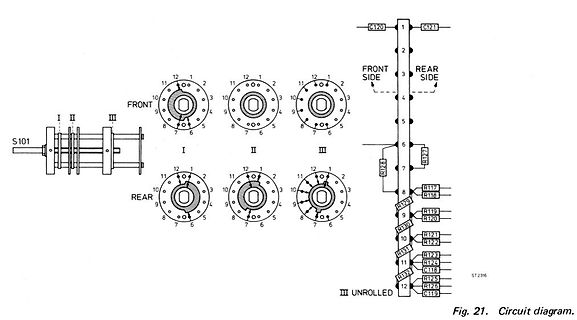
S101 I II III FRONT REAR 12 1 11 2 10 3 9 4 8 5 7 6 I II III FRONT SIDE REAR SIDE C120 C121 2 3 5 6 R127 R128 7 8 R117 R118 R129 9 R120 R130 10 R121 R122 R131 11 R123 R124 R132 C118 12 R125 C119 III UNROLLED Fig. 21. Circuit diagram.
-
 Bild
Erklärung elektrischer Downtilt bei Antennen mit Diagrammen
illustrates the effect phase shifting has on the direction of the main lobe. AF Main beam Phase shift nulls side lobe Max radiation Cartesian plot Polar plot $\phi=0$ Figure 5, Antenna elements phase shifts The antenna's "electrical" downtilt is actually accomplished mechanically, as the phase shifters are adjusted

-
Thread
Wer kann mir helfen, wer kennt diese Punktmatrix
10 pins und I2C-Bus: https://newhavendisplay.com/de/2x16-character-cog-lcd-stn-blue-display-with-side-white-backlight-3v/ hier ist pin 10 links, dafür ist z.B. der Reset auf der anderen Seite
-
 Bild
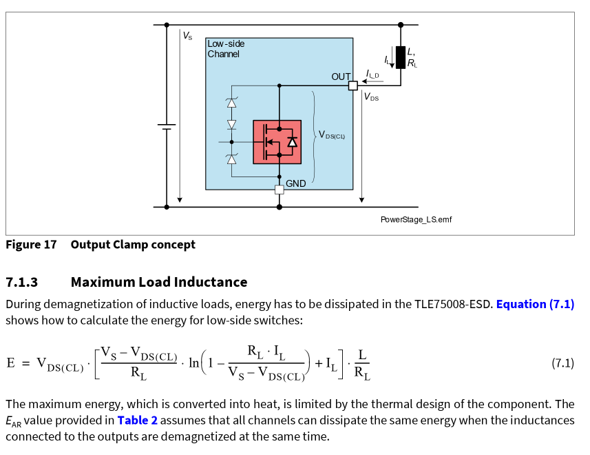
Schaltplan Output Clamp Konzept und Energieformel
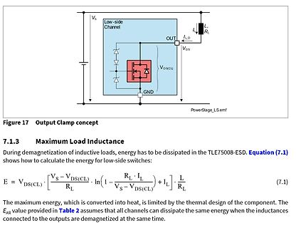
has to be dissipated in the TLE75008-ESD. Equation (7.1) shows how to calculate the energy for low-side switches: E = VDS(CL) * [ (VS - VDS(CL)) / RL * ln(1 - IL * (VS - VDS(CL)) / RL) + IL ] * L / RL (7.1) The maximum energy, which is converted into heat, is limited by the thermal design of the component
-
 Bild
Produkttabelle für integrierte LED-Controller
Controller within LED PN: 1312020030000 1313210530000 1312121320437 1315050930002 Size: 2020 Chip LED 3210 Side View 2121 PLCC6 5050 PLCC4 MSL: MSL 3 MSL 3 MSL 5a / IPx7 MSL 3 PWM level / per color: 8-bit 8-bit 12-bit 8-bit Product Picture:

-
Thread
Bemaßung 80mm China BGA Stencil
www.ly-store.com/reball-jig-reball-station/80mm-90mm-stencil-common-use-auto-lock-accurate-position-multi-sides-adjustment-easy-operation-p60088.html Und es geht um die Bohrungen für die Befestigungen, wie sie auf den Bildern zu sehen sind. Leider habe ich keine Zeichnung mit Bemaßung gefunden, welchen Durchmesser
-
Thread
Suche IC Datenblatt
#7621979: > PWM Treiber Dafür wären die Transistoren ganz ungeschickt verschaltet, denn die Low-Side Transistoren gegen Masse schalten nur langsam ab, weil ihre Basis sich selber "ausräumen" muss. Torsten B. schrieb im Beitrag #7621987: > BH2228FV Ah, also zum "Glück" keine PWM, sondern eine rein
-
Thread
Dämmerungsschalter Prüfungsaufgabe Ausbildung
Beitrag #7619064: > Ich hoffe, dass -Q1 > mehr als einen Hauptkontakt haben darf... Oder ein Low-Side-Schalter machen... Ich schätze aber, das ist nicht zulässig, aber ich bin kein Elektriker...
Wolfgang R. schrieb im Beitrag #7619067: > Oder ein Low-Side-Schalter machen... Ich schätze aber, das ist nicht > zulässig, aber ich bin kein Elektriker... Ne, N schalten ist doof, weil dann der N von den Lampen bis zum Schütz im ausgeschalteten Zustand auch
-
 Bild
Schaltplan einer Sololuchte
C1 560k R4 910k R3 (ST)69015 Q2 470 R7 LED D1 yellow ultra-bright LED D2 yellow ultra-bright 30 R (sid) R8 (ST)6914 Q1 SL-6 JC-01 TO-92 Q1; Q2 E B C C E

-
 Bild
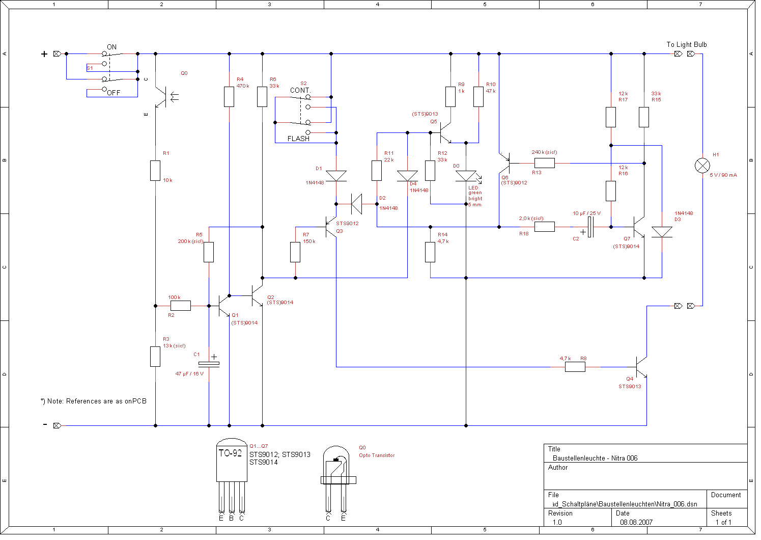
Schaltplan einer Bausteuchte
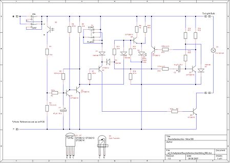
ON OFF Q0 R4 470k R6 33k CONT FLASH D1 1N4148 (STS)6013 Q5 R11 22k R12 33k R10 47k 240 k(sid) R17 12k R15 33k H1 5V / 90mA D2 1N4148 D3 1N4148 LED 5mm bright R13 12k R16 12k R18 2,0 k(sid) C2 10uF/25V Q6 (STS)6012 R7 180k Q3 (STS)6014 R14 4,7k R2 100k R3 13k (sid) C1 47uF/16V Q1 (STS)6014 Q2 R5 200k (sid) R8 4,7k Q4 STS9013 TC-92 STS9012 STS9013 STS9014 Q0 Opto Translator E B C C E Title Bausteuchten- Nitra 006 File kd_SchaltplaeneBausteuchtenNitra_006.dsn Revision 1.0 Date 08.08.2007 Sheets 1 of 1
-
Thread
Ampelschaltung
ich habe ein kleines Problem mit einer Ampelschaltung. Die Schaltung für die zwei Ampeln (main und side) funktionieren. Jetzt wollte ich eine Fußgängerampel integrieren die folgendes tun soll: - nach dem drücken des BTN0 wird ein Merker gesetzt - Wenn die Ampel Main im State Green ist, soll die Fußgängerampel
-
 Bild
Blockschaltbild eines MSL9512RS Mikrocontrollers
LATCHES RESET "O" SUPPRESS CONTROL 9 SP 10 10^4 10^3 10^2 10^1 10^0 "O" SUPPRESS FLAG CLOCK S/P 8 SID/ PID8 8 4 2 1 DP 8 4 2 1 DP 8 4 2 1 DP 8 4 2 1 DP 2 PID6 SHIFT 5 PID4 25 BIT SHIFT REGISTER 4 PID2 WITH S/P CONTROLLER 3 PID1 Vcc 14 GND

-
Thread
Arduino, Wilderness Labs, Emteria und Co - Updates auf ganzer Front
access these crucial points on the board. We introduced a new VUSB soldering jumper on the top side, allowing you to conveniently enable the VUSB pin while using the castellated pins. In addition, the Nano 33 BLE Rev2 transitions the power supply component to the MP2322 to guarantee increased
The biggest design change in the UI of emteria Device Hub is the move of the navigation bar to the side (1). Not only does this look better but creates more space to introduce new features. [/c] ### QT for MCU fortan auch auf Infineon-Chips. Das „QT for MCU“ mit QT eigentlich nur den QML-Parser
-
 Bild
Dashboard der Emteria Software-Verwaltung
EMTERIA Dashboard 1. SIDE NAVIGATION 2. QUICK ACCESS TO PRE-FILTERED DEVICES Monitor device status and events Policy compliance Enrolled devices Online status 3. FILE UPLOAD FOR APP 4. NEW GROUP MANAGEMENT Device activity OS

-
Thread
ATtiny85 I²C Slave übernimmt empfangenen Wert nicht.
can detect stop condition (http://www.avrfreaks.net/index.php?name=PNphpBB2&file=viewtopic&p=984716&sid=82e9dc7299a8243b86cf7969dd41b5b5#984716) * it needs to be called in a very tight loop in order not to miss any (REMINDER: Do *not* use delay() anywhere, use tws_delay() instead). * It will
-
Thread
HighSide-Treiber AUIR3242STR
Hallo zusammen, das Projekt ist ein MPP-Laderegler. Das MPP-Tracking und den Buck-Converter habe ich mit dem IR2104 und entsprechend Highside- und Lowside N-MOSFET vom Typ CSD19505 umgesetzt. Nun zur eigentlichen Problemstellung: Mit dem Buck-Converter lade ich meine Batterie. Zum Entladen über einen Wechselrichter ist ein Highside-N-MOSFET geplant (CSD19505). Da ich noch nicht sicher bin, ob der Wechselrichter mit der PWM klar kommt, brauche ich einen Treiber, der sowohl den statischen als auch den dynamischen Fall abdeckt, was ja bekanntlich mit dem IR2104 und der Bootstrap-Schaltung nicht
-
Thread
3 x INA114 am selben Shunt?
in der Plusleitung einsetzbar! Der INA219 kann bis 26 Volt am Eingang, aber taugt nichts für LowSide. Der INA114 scheint noch mehr Spannung zu können. Tim schrieb im Beitrag #7613417: > Was Unfug ist, wie mir gerade klar wurde, da ich nämlich totalen Mist > gerechnet hatte. Natürlich klappt das
-
 Bild
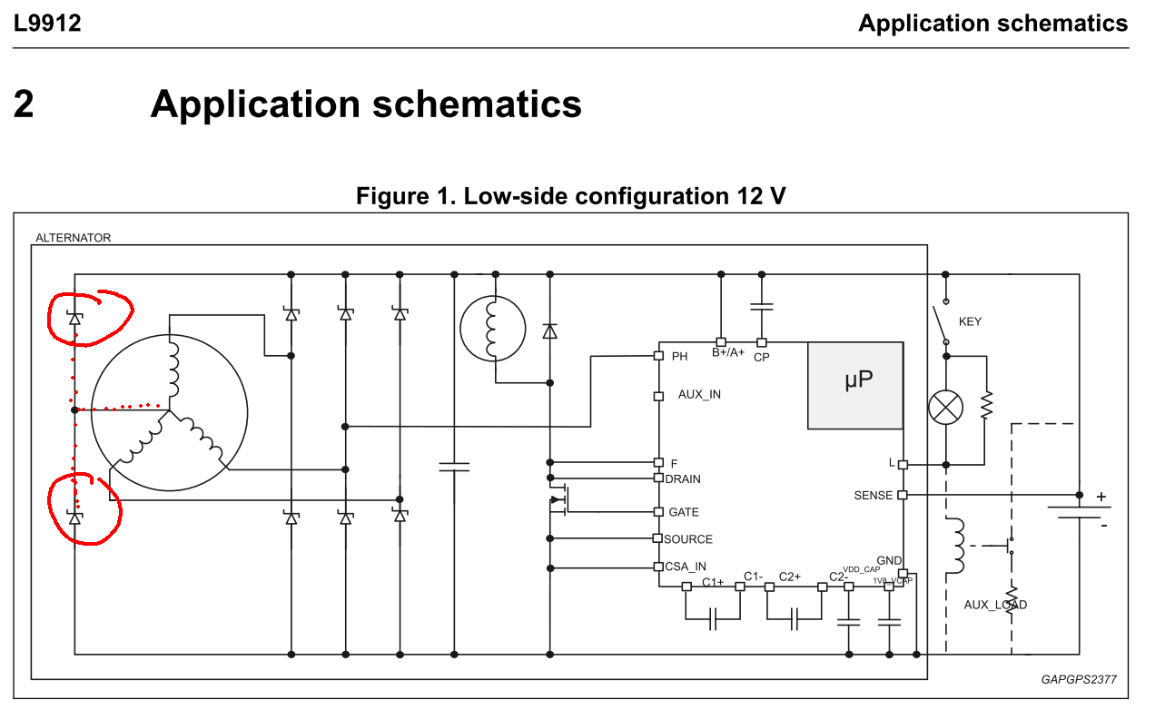
Schaltplan einer Low-side Konfiguration 12 V für einen Alternator
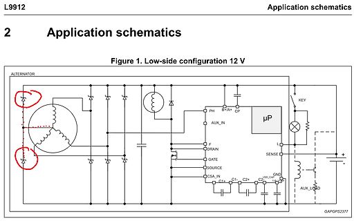
L9912 Application schematics 2 Figure 1. Low-side configuration 12 V ALTERNATOR KEY μP L SENSE GND AUX_LOAD + AUX_IN F DRAIN GATE SOURCE CSA_IN C1+ C1- C2+ C2- VDD_CAP GND 1V8
-
Thread
Verständnisproblem PNP-Transistorverstärker Drawdio
Im Zusammenhang mit Obigen, ist mir die Verstärkerschaltung insgesamt nicht ganz transparent (High-Side-Switch?). Ich würde davon ausgehen, dass diese einen Basiswiderstand benötigt um den maximalen Strom, der in den Timerausgang fließt, zu begrenzen (oder ist dieser vom Ausgangswiderstand des Timers
-
 Bild
Bestückungsdruck einer Kopfhörer-Leiterplatte
R1, R3, W4, R4, L4, JK2, L5, L6, HEADPHONES PCB 440.00.0485 ASSY 590.05.0161, View from component side

-
Thread
Farbgebung des Arduino Editors
Click on the theme to open its extension page. Click the "Download Extension" link on the right side of the page. Wait for the download to finish. Install Theme in Arduino IDE The downloaded file will have the .vsix file extension of VS Code extensions. This file is really a ZIP archive. It must
to customize from the menu on the left side of the page. Select the color you would like for that component. You will see a preview of how it looks in the simulated VS Code window on the page. Repeat until you have finished your customizations
-
Thread
Stromsensor stabilisieren ACS712x
Aufbauten mit dem INA219, Deinem ähnlich, und war von dessen Genauigkeit fasziniert. Natürlich high-side, man will nicht unbedingt GND verschieben. Jörg R. schrieb im Beitrag #7607713: > Es gibt hier im Forum einen sehr interessanten und ausführlichen > Kommentar zum Thema ASC712, ich meine vom User
-
 Bild
Leiterplatten-Layout und Leiterbahnenansicht TDA1072A
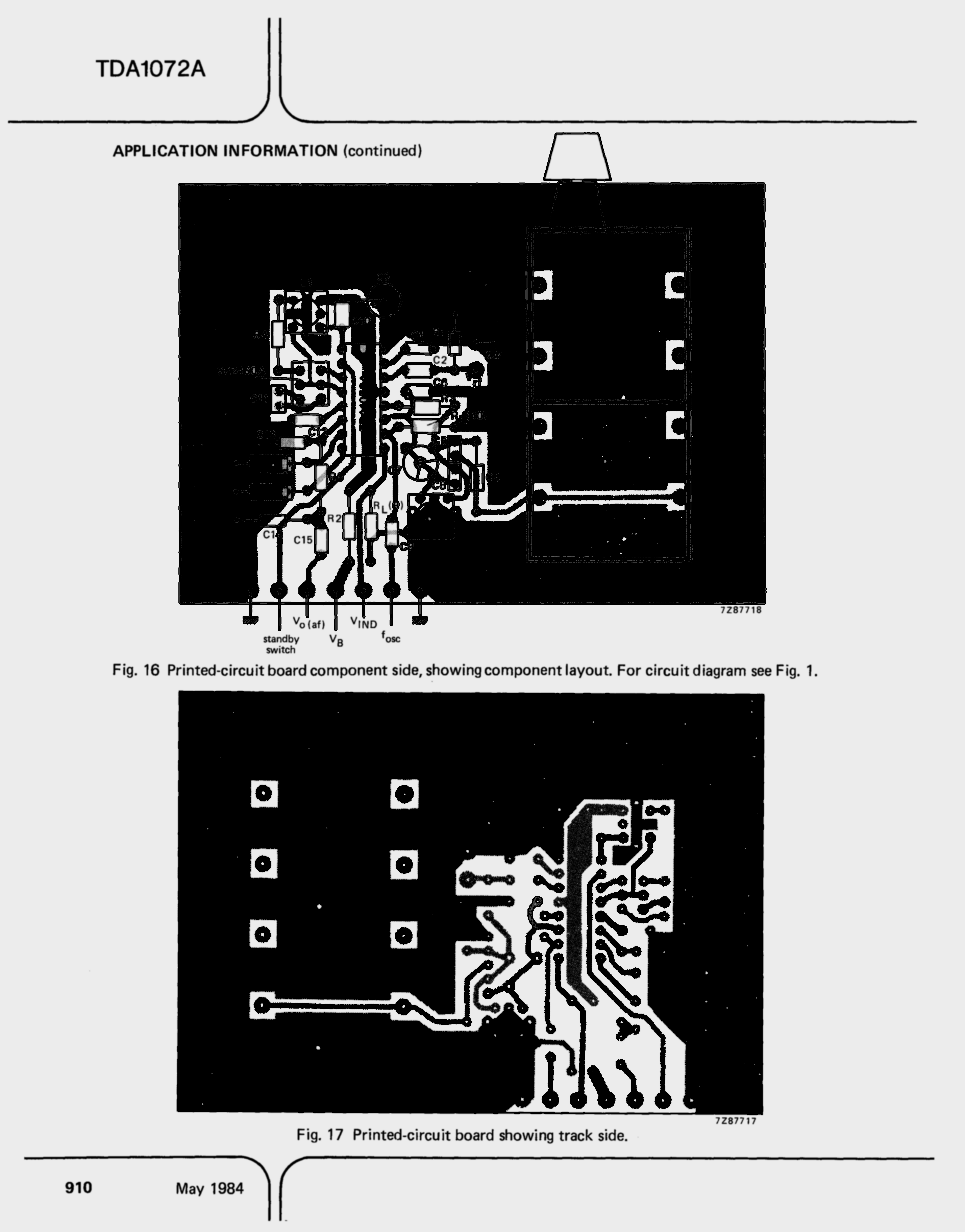
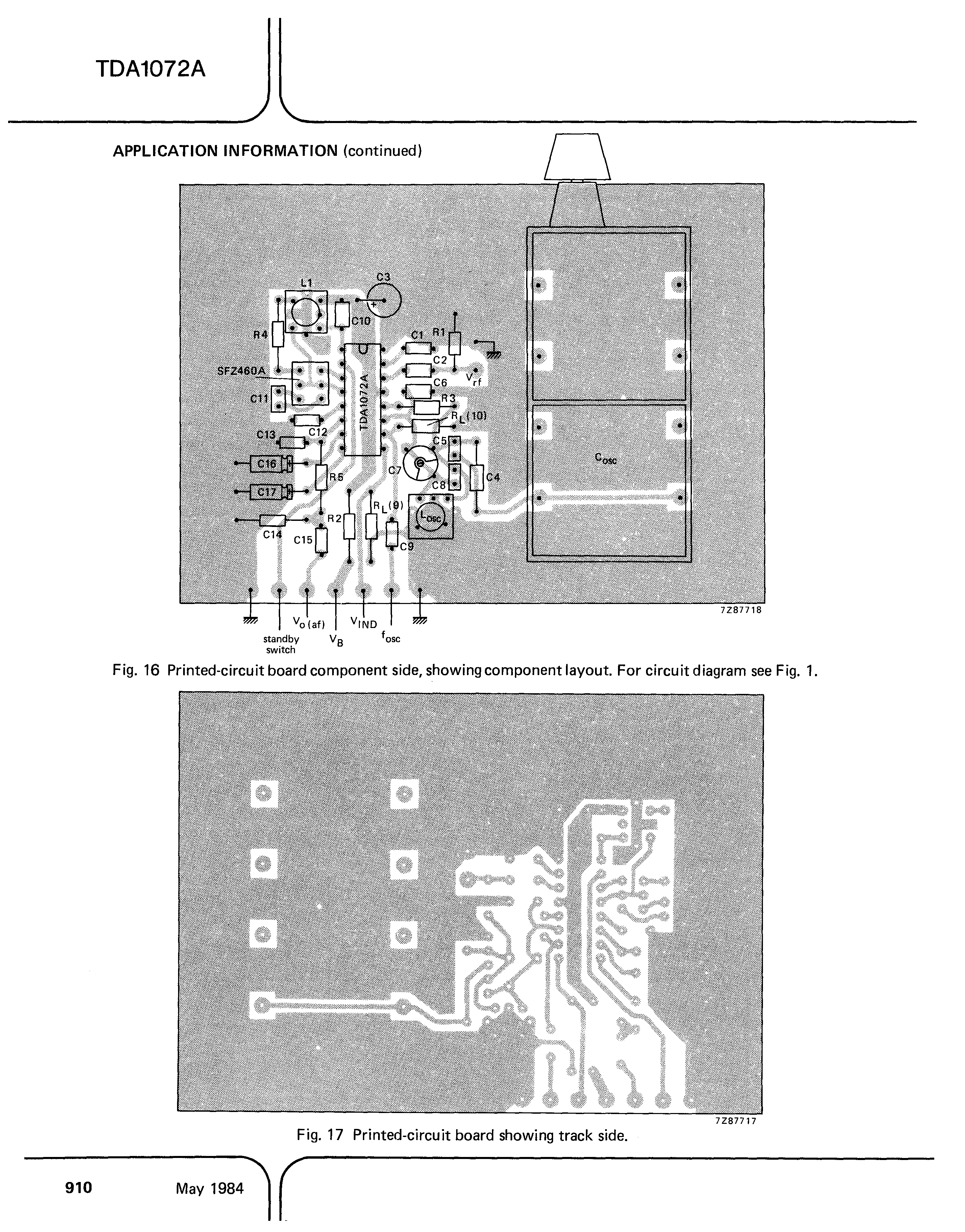
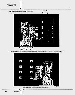
C14, C15, R1, R2, Vo (af), standby switch, VB, VIND, fosc Fig. 16 Printed-circuit board component side, showing component layout. For circuit diagram see Fig. 1. 7Z87716 Fig. 17 Printed-circuit board showing track side. 7Z87717 910 May 1984
-
Thread
Überschwinger beim Verbinden der Stromversorgung
droht so ein Szenario immer – und bei den Step-Down-Synchron-Schaltreglern mit einem N-MOSFET im High-Side, die eigentlich immer an dem Bootstrap-Kondensator gut erkennbar sind, ist das nur eine Frage der Zeit, bis etwas passiert und sich der Regler dann selbstkillt. Es gibt selbstverständlich noch andere
-
Thread
high side gate driver
Ludwig M. schrieb im Beitrag #7606073: > Wer kennt einen high side gate driver, der sich hierfür eignet? Er > sollte möglichst „üblich“ (und nicht teuer) sein. Welcher MOSFET eignet > sich? Der Peak-Strom kann im Puls bis 1A gehen (im Dauerbetrieb können > die LEDs
Gatetreiber einsetzen? Deine eingezeichneten Mosfets sind N-Channel? Bewusst so gewählt für HighSide?
-
 Bild
Handgezeichnetes Blockschaltbild eines LED-Treibers mit Gate-Drivern
4x high side gate drivers +5V 4 Gruppen 8x RGB LED driver STP24DP05 LED0 LED1 LED7

-
 Bild
Bestückungs- und Leiterseiten einer Leiterplatte
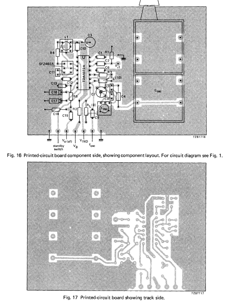
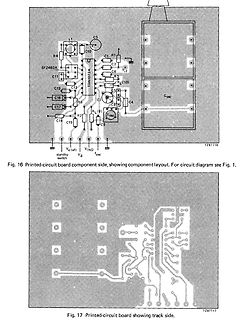
RL(0) Losc C9 R2 C14 C15 V0(af) VIND fosc standby switch Fig. 16 Printed-circuit board component side, showing component layout. For circuit diagram see Fig. 1. 7287718 Fig. 17 Printed-circuit board showing track side. 7287717
-
 Bild
Leiterplatten-Layout und Leiterbahnen des TDA1072A
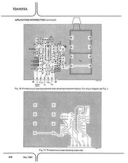
C16 C17 C12 C13 R6 C11 C14 C15 R2 C9 V0 (af) VIND V_B f_osc Fig. 16 Printed-circuit board component side, showing component layout. For circuit diagram see Fig. 1. 7Z87716 Fig. 17 Printed-circuit board track side. 7Z87717 910 May 1984
-
 Bild
Datenblattseite eines AM-Empfänger-Schaltkreises
Semiconductors Product specification AM receiver circuit TDA1072A Fig.17 Printed-circuit board showing track side. 1267117 May 1984 17

-
 Bild
Bestückungsdruck einer Leiterplatte mit Montagehinweisen
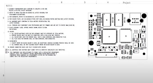
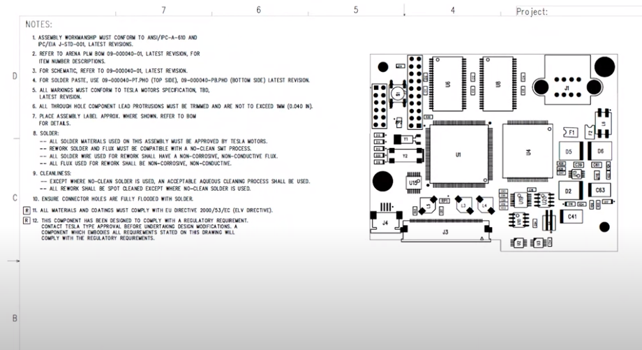
01, LATEST REVISION, FOR ITEM NUMBER DESCRIPTIONS. 3. FOR SCHEMATIC, REFER TO 09-000040-P.PHO (TOP SIDE), 09-000040-P.PHO (BOTTOM SIDE) LATEST REVISION. 4. FOR SOLDER PASTE, USE 09-000040-P.PHO. 5. ALL MARKINGS MUST CONFORM TO TESLA MOTORS SPECIFICATION, TBD, LATEST REVISION. 6. ALL THROUGH-HOLE COMPONENT