the on-board PCB antenna is 2 dBi. Espressif 27/30 2018.12 3. ESP8266EX Module Figure 3-2. ESP-WROOM-02 Module For details of ESP-WROOM-S2, please refer to ESP-WROOM-02 Datasheet. 3.3. ESP-WROOM-02D/ESP-WROOM-02U The module size of ESP-WROOM-02D is (18±0.2) mm x (20±0.2) mm x (3±0.15) mm. The type of flash
> https://www.voelkner.de/products/657827/STMicroelectronics-Entwicklungsboard-NUCLEO-F103RB.html?ref=43&gclid=EAIaIQobChMI47DK157o3wIVg9GyCh0SMQltEAQYAyABEgJDlvD_BwE > > Da bekommst du ganz regulär für 12 Euro ein originales (!) Development > Board mit einem 32bit Mikrocontroller einschliesslich
time_t now = time(nullptr); struct tm * timeinfo; timeinfo = localtime(&now); Serial.printf("%02d:%02d:%02d",timeinfo->tm_hour,timeinfo->tm_min,timeinfo->tm_sec); Serial.println(); [/code] Einfacher geht doch nicht. Gruß aus Berlin Michael
0,38Nm http://www.pollin.de/shop/dt/NTE0OTg2OTk-/Motoren/Schrittmotoren/Schrittmotor_VEXTA_PXB44H_02AA_C8_1_8_6_V_0_8_A.html 0,9 Nm http://www.pollin.de/shop/dt/NTQ1OTg2OTk-/Motoren/Schrittmotoren/Schrittmotor_PSM57BYGHM201_0_9_.html > Des Weiteren würde ich den Motor gerne vom PC aus ansteuern
|(1<<ADPS1); // Frequenzvorteiler ADMUX = mux; // Kanal waehlen //ADMUX |= (1<<REFS1) | (1<<REFS0); // interne Referenzspannung nutzen /* nach Aktivieren des ADC wird ein "Dummy-Readout" empfohlen, man liest also einen Wert und verwirft diesen, um den ADC "warmlaufen zu lassen
in aus dem Code ersichtlich, er immer den Wert 1023 annimmt (AVcc ist 5V, Aref ist 0,07V, Vin ist 0,02V). Ich bin wirklich am verzweifeln, von den Spannungen her dürfte er ja netmal die hälfte des Messbereichs ausschöpfen? Kann mir bitte einer Weiterhelfen ? Vielen Dank im Voraus.
fotographiert. es dauert ganz schön. schaut es euch mal unter http://opabastelkram.blogspot.com/2010/02/blog-post.html an. ach und wenn ich wirklich mal vergleiche habe ich auch mehr kleinteile als meine freundin :-)
wirklich goldwert (z.b. TCA965 der locker 10eur kostet), ich sehe auch einige alte und seltene opamps/ref. ics. Eine liste machen würde sich lohnen, kistenweise verkaufen würde ich nciht machen. Respekt vor dem Opa, schade nur das du nicht "vorsetzen" kannst/möchtest.
Schau hier, dort wurde auch eine PWM-Steuerung als Möglichkeit erwähnt. https://ebrnd.de/2016/02/in-9-bargraph-nixies-pt-1
R und einer nach dem R. Die Differenz ist zwar klein aber dafür hast du ja den GAIN x200 und die REF von 1,1V. Du musst nicht auf hohe Spannung kommen.
ensure state of the art GPS receiver performance and accuracy. Page 34 of 43 User’s Manual V3.2 - 02/06 GPS Receivers A1029 11 Applications and Hints 11.1 Minimum Configuration Please refer to chapter 3.1 Minimum Configuration for details. In addition, for opti- mized start-up behavior it is strongly
is approximately equal to 2 Q. Session: One byte, Session value,range is 0-3. 0x00:S0; 0x01:S1; 0x02:S2; 0x03:S3; MaskMem: One byte. It specifies the target memory when applying inventory mask with 0x01 for EPC memory, 0x02 for TID memory and 0x03 for User memory. Other values are reserved. MaskAdr:
_RE2_REF_RA3 0xA //!old only provided for compatibility #define ANALOG_NOT_RE1_RE2_REF_RA3_RA2 0xB //!old only provided for compatibility #define A_ANALOG_RA3_RA2_REF 0xC //!old only provided for compatibility #define RA0_RA1_ANALOG_RA3_RA2_REF 0xD //!old only provided for compatibility #define RA0_ANALOG 0xE //!old only provided for compatibility #define RA0_ANALOG_RA3_RA2_REF 0xF //!old only provided for compatibility // Constants used in
Distortion 1.56MHz into CH0. Also Applicable to CH1 and CH1 Code-to-Code V = 2.5V (Note 17) 0.25 1 LSB REF RMS Transition Noise Full Power Bandwidth VIN 2.5VP-P SDO = 11585LSBP-P(–3dBFS) (Note 15) 50 50 MHz Full Linear BandwidthS/(N + D) 68dB 5 5 MHz U U U I TER AL REFERE CE CHARACTERISTICS TA= 25°C. VDD
Funktionsgeneratoren mit 12 Bit DA-Wandler. Diese haben beide einen ( gemessenen ) Klirrfaktor von 0,02% bei Frequenzen kleiner als 100KHz. Ralph Berres
Klirrfaktormessbrücken Unsere Messkisten hatten eine Referenz Funktion. Zuerst wurde der Messsender gemessen, REF gedrückt, dann die Übertragungsstrecke gemessen. Der dann abgelesene Wert entsprach der eher der Realität.
CHECKED APPROVED DESIGN CONTROL STATUS BY: BY: BY: DATE: YR/MO/DAY J M.NABEI M.SASAO M.SASAO 2004/02/02 DOCUMENT NUMBER FILE NAME SHEET PS-54132-058 PS-54132-058.doc1 OF 8 EN-37(019) LANGUAGE PRODUCT SPECIFICATION JAPANESE ENGLISH 4. PERFORMANCE 4 - 1. Electrical Performance Item Condition Standard
nicht größer ist als bei einer normalen Skalierung mit einem krummen Wert, etwa von der Umrechnung der Ref. Spannung oder Taktfrequenz. Das kann vor allem dann hilfreich sein, wenn der µC Hardware Multiplikation kann, oder eine Multiplikations-routine sowieso schon da ist.
power mode (refer to Start and Stop Definition timing diagram). ACKNOWLEDGE: All addresses and data words are serially transmitted to and from the EEPROM in 8-bit words. The EEPROM sends a zero during the ninth clock
AVDD in presence of external # AVDD supply w 30 01 08 # Enable Master Analog Power Control w 30 02 00 # Set the input powerup time to 3.1ms (for ADC) # w 30 47 32 # Set the REF charging time to 40ms w 30 7b 01 ############################################### # Playback Setup ################
30 36 40 # Route IN_1R to Right MicPGA P w 30 37 40 w 30 39 40 # Mixer Amp -> HP outs w 30 0C 02 02 # Mixer Amp -> Lineouts w 30 0E 02 02 # PGA Bypass Gain = 0dB w 30 18 00 00 # Power up HPL/HPR, LOL/LOR and MAL/MAR drivers w 30 09 3F # Unmute HPL/HPR driver, 0dB Gain w 30 10 00 00 # Unmute
heute ein Step Up Converter das Mittel der Wahl, z.B. https://www.amazon.de/gp/product/B08BLKPDDJ/ref=ppx_yo_dt_b_asin_title_o02_s00?ie=UTF8&psc=1&pldnSite=1 Aber zurück zum Artikel. Bei plötzlichem Spannungsanstieg an einer Spule ist ein Überschwingen auf das Doppelte der Betriebsspannung ansich
ein Step Up Converter das Mittel > der Wahl, z.B. > https://www.amazon.de/gp/product/B08BLKPDDJ/ref=ppx_yo_dt_b_asin_title_o02_s00?ie=UTF8&psc=1&pldnSite=1 Für welche Aufgabe genau? Worauf bezogen? Auf obiges, oder "Deine"? > Aber zurück zum Artikel. Vermutlich "zum Threadthema". > Bei
AM3+ CPU you adopt. If you want to adopt DDR3 1866/1600 mem- ory module on this motherboard, please refer to the memory support list on our website for the compatible memory modules. ASRock website: http://www.asrock.com 4. Due to the operating system limitation, the actual memory size may be ® less than
Nimm doch von C. zum Beispiel: Aussenpumpe "Extra" 1005.02.00 » Best.-Nr.: 570265 - 62 oder Barwig Hochleistungs-Außenpumpe 02 » Best.-Nr.: 537454 - 62 * Max. Förderhöhe 10 m * Max. 20 l/min. Die sind bei U-nenn natürlich nicht für Dauerbetrieb
z.B. folgende nehmen: http://www.amazon.de/Eheim-2213010-Aussenfilter-Classic-2213/dp/B000A2166A/ref=sr_1_1?ie=UTF8&s=pet-supplies&qid=1304338111&sr=8-1 Kann man zwar nicht regeln, aber ist simpel, relativ günstig und man kann sogar noch Filter zur Wasserreinigung einbauen. Gruß Tobias
MCU_DBG Register, die liefert als Revision 0x2000, das sollte es aber beim F051 gar nicht geben laut RefMan.
Register, die liefert als > Revision 0x2000, das sollte es aber beim F051 gar nicht geben laut > RefMan. Das ist ein ziemlich sicheres Zeichen daß das welche sind, bei denen die initiale Programmierung in der Fabrik von ST nicht korrekt durchgelaufen ist.
für den kleinen Bruder ICL7103 beschrieben https://www.intersil.com/content/dam/Intersil/documents/an02/an028.pdf Eine Variante des ICL7103 war übrigens im ersten Hand-Digitalmultimeter dass man kaufe konnte drin (Fluke 8020A in 1977). Heute noch ist eine Variante des Chips das Herz tödliche 3 Euro
. https://www.amazon.de/AD584-Hochpr%C3%A4zises-Spannungsreferenzmodul-4-Kanal-10/dp/B07TSTGZR5/ref=sr_1_fkmr0_1?__mk_de_DE=%C3%85M%C3%85%C5%BD%C3%95%C3%91&keywords=ad584+dip8&qid=1574007467&sr=8-1-fkmr0 Kostet weniger als die Hälfte. Könnte man das versuchen oder geht das in die Hose?
CONDITIONS MIN TYP MAX UNIT -VDET(S) -VDET(S) Detection Voltage (Note 1) -VDET 1 ×0.98 -VDET(S)×1.02 V -VDET -VDET -VDET Hysteresis Width V HYS 1 ×0.02 ×0.05 ×0.08 V Current Consumption ISS 2 VDD 2.0V 2.5 μA Operating Voltage VDD 1 0.95 10.0 V Output Current I 3 Output transistor 0.23 0.64 mA OUT Nch
scope of this application note. A Quick Start Guide is found last in this document. Rev. 2555C-AVR-02/04 Theory of operation – the internal RC oscillator In production the internal RC is calibrated at either 5V or 3.3V. Refer to the datasheet of the individual devices for information about the operating
scope of this application note. A Quick Start Guide is found last in this document. Rev. 2555C-AVR-02/04 Theory of operation – the internal RC oscillator In production the internal RC is calibrated at either 5V or 3.3V. Refer to the datasheet of the individual devices for information about the operating
L A 0.05 M E 0.02 H 1 T 0.01 N I S SINGLE PULSE A R0.1 ,) 0.00001 0.0001 0.001 0.01 0.1 1 10 100 1000 ( t, TIME (S) R Figure 8. Thermal Response, Junction−to−Ambient (1 inch pad) http://onsemi.com 3 MBRS410LT3 PACKAGE
D7 D6 D5 D4 D3 D2 D1 D0 DAC data register VREF - AGND 7 i VAOUT VAOUT = AGND + Di 2 256 i = 0 VDD V REF V AGND VSS 00 01 02 03 04 FE FF HEX code Fig.7 DAC data and DC conversion characteristics. handbook, full pagewidth MBL828 PROTOCOL S ADDRESS 0 A CONTROL BYTE A DATA BYTE 1 A DATA BYTE 2 A SCL 1 2 8
PIPELINE ADC E OUTPUT D9–D0 Digital Set-Top Boxes IN- C DRIVERS Video Digitizing Applications OVDD PD REF REF SYSTEM + BIAS OGND REFOUT REFIN RECOM REFN OE Pin Configuration appears at end of data sheet. ________________________________________________________________ Maxim Integrated Products 1 For free
so...ich habe jetzt mal eine Messung durchgeführt und bin quasi entsetzt. 1. Messung: 600mA 5,02V (in etwa das Ergebnis wie beim laufenden Pi) 2. Messung: 1,7A 4,9V (aber meist weniger) mit starkem Brummen 3. Messung: 2,8A 4,14V und die Platine fing an zu schwingen. Kurze Zeit später ging dann
: http://www.amazon.de/AIPowerTM-Ladeger%C3%A4t-Ladeadapter-Smartphones-USB-ladende/dp/B00JDGU9WQ/ref=pd_sim_147_5?ie=UTF8&dpID=31VDmDr4HvL&dpSrc=sims&preST=_AC_UL160_SR160%2C160_&refRID=1RYCCE1ESWJ3BC4YKKNK Dann müsste ich nur noch ein USB-Kabel auf Stromversorgung vom Hub basteln. In der Hoffnung
Response –Type 2 Figure 47 ADC Digital Filter Ripple –Type 2 0.02 0 0.01 -20 0 B B -0.01 ( -40 ( e e n n -0.02 s s e e R -60 R -0.03 -0.04 -80 -0.05 -100 -0.06 0 0.5 1 1.5 2 2.5 3 0 0.05 0.1 0.15 0.2 0.25 Frequency (Fs) Frequency (Fs) Figure 48 ADC Digital Filter Frequency
Response –Type 2 Figure 48 ADC Digital Filter Ripple –Type 2 0.02 0 0.01 -20 0 B B -0.01 ( -40 ( e e n n -0.02 s s e e R -60 R -0.03 -0.04 -80 -0.05 -100 -0.06 0 0.5 1 1.5 2 2.5 3 0 0.05 0.1 0.15 0.2 0.25 Frequency (Fs) Frequency (Fs) Figure 49 ADC Digital Filter Frequency
--- 15 ~ 20 13. INSPECTION CRITERION -------------------------------------------1 ~ 30 02101300-01-02 E M E R G I N G D I S P L A Y MODEL NO. VERSION PAGE TECHNOLOGIES CORPORATION E T 0 3 5 0 G 0 D H 6 6 1 1. GENERAL SPECIFICATIONS 1 . 1 APPLICATION NOTES FOR CONTROLLER/DRIVER PLEASE REFER TO : H X 8

 Bild
Bild
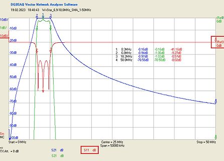
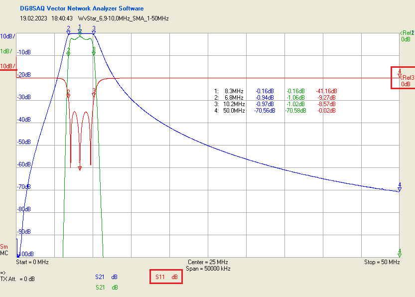
 Bild
Bild