-
Thread
CH32V003 Resetverhalten
condition to ensure that the system is in supply. It works when the power exceeds 2.7V; when VDD is lower than the set threshold (VPOR/PDR), the device is placed in the reset state without using an external reset circuit. In addition, the system is equipped with a programmable voltage monitor (PVD
volatile int i; doof: GPIOA->BSHR = (1<<2); // PA2 = grüne LED auf High setzen i=100000; while(i-- > 0); GPIOA->BSHR = (1<<16) | (1<<(16+2)); //grüne LED auf low=aus setzen i=100000; while(
-
Thread
Schulprojekt Elektronisch stabilisiertes Netzteil
Vielleicht ganz interessant: Aber bei den Low-Drop gibt es noch mehr Spezialliteratur dazu. Und: Bei Digitalschaltungen ist also die Faustregel "pro TTL-IC ein 0,1µF Kondensator" auch nicht mehr der absolute "state of the art". Die Gesamtkapazität
pin. The load or feedback must consume this minimum current for regulation or the output may be too high. A 250-Ω feedback resistor between OUTPUT and ADJUST consumes the worst case minimum load current of 5 mA..." Also auch vorher überlegen, wieviel Strom gezogen werden soll. Zur Not einen Widerstand
-
 Bild
Bild
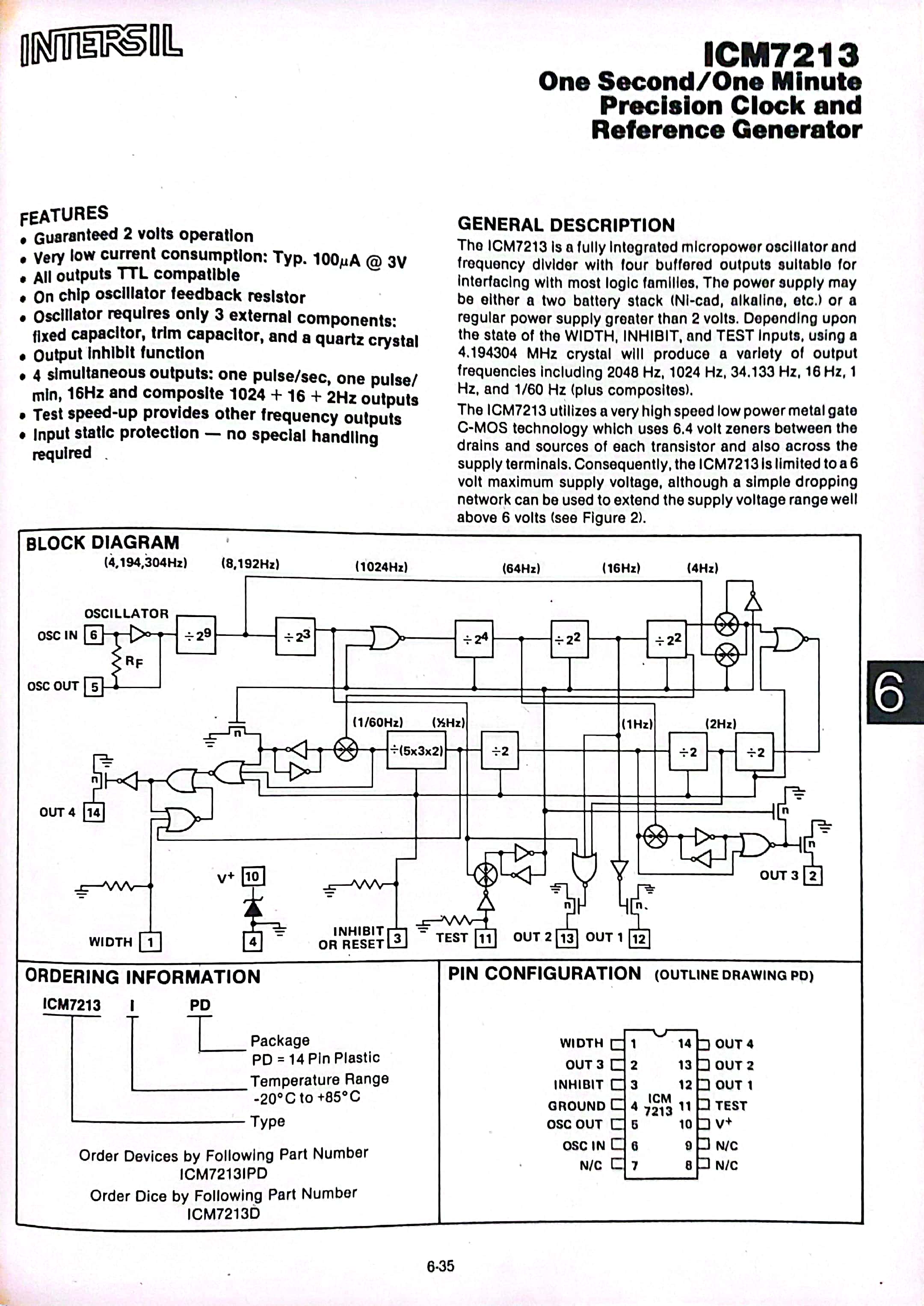
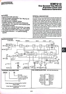
Datenblatt ICM7213 Precision Clock and Reference Generator
Second/One Minute Precision Clock and Reference Generator FEATURES Guaranteed 2 volts operation Very low current consumption: Typ. 100uA @ 3V All outputs TTL compatible On chip oscillator feedback resistor Oscillator requires only external components: fixed capacitor, trim capacitor, and a quartz crystal
-
Thread
6502 sound generation
digitalen Signalverarbeitung moeglichst "vorher" machen zu lassen, dann in Sachen "digitale Filter" auf low-End-CPUs kann man zwar schon das ein- oder andere machen, aber so richtig dolle wirds keinesfalls. Gruss WK
ergibt sich eine kontinuierlich ändernden PDM. In der gefilterten Version ist das ein Dreieck, je nach High-Cut geht es Richtung Sinus. Der Ton im mp3 hört sich nicht so an. Da höre ich zwei Töne. Exor involviert?
-
Thread
Zuschalten oder kurzschließen
Dein Halbbrückentreiber mit Bootstrap-Stromversorgung kann nur eine endliche Zeit HIGH schalten. Denn irgendwann ist der Pufferkondensator der Oberstufe zu sehr entladen (Mikro-Millisekunden). Dann muss die Halbbrücke wieder kurz LOW schalten. LOW kann sie unbegrenzt schalten, denn dabei
einer galvanisch getrennten Versorgung mittels DC/DC Wandler für die Oberstufe kann die unbegrenzt HIGH schalten.
-
Thread
Temperaturabhängigkeit der Basisspannung eines Transistors
Germanium-Transistor, ist es die Hälfte? coefficient of Germanium is approximately -2.5mV / C, slightly higher than for Silicon which have a typical temperature coefficient of - 2mV / C, Silicon Schottky diodes have a lower temperature coefficient of -1.45mV / C.
. schrieb im Beitrag #7879085: > coefficient of Germanium is approximately -2.5mV / C, slightly higher > than for Silicon which have a typical temperature coefficient of - 2mV / > C, Silicon Schottky diodes have a lower temperature coefficient of > -1.45mV / C. Ja, und was größer und kleiner
-
Thread
Kapazitiver Taster einer Ampelsteuerung
Wer mag, kann auch einen Komparator nehmen um die Spannung am Widerstand zu erfassen, oder einen High Side Current Sensor, irgendeine INA halt. Oder die Elektronik untersuchen, reichlich sicher ist da ein Transistor drin der einen Lastwiderstand schaltet. Den kann man rausknipsen und stattdessen
mag, kann auch einen Komparator nehmen um die > Spannung am Widerstand zu erfassen, oder einen High Side Current Sensor, > irgendeine INA halt. > > Oder die Elektronik untersuchen, reichlich sicher ist da ein Transistor > drin der einen Lastwiderstand schaltet. Den kann man rausknipsen und
-
Thread
Gibt es Elektretmikrofone mit D > 10mm
diese Website zu kömmen, wo das Teil vorgestellt wird. mfg https://thatcorp.com/that-1510-1512-low-noise-high-performance-audio-preamplifiers/
-
Thread
Assembler Programm von ATtiny13 auf ATtiny45 portieren
Welche Fuses sind denn gesetzt? Nur die, die standardmäßig bei den µCs gesetzt sind. Ext 0xFF HIGH 0xD7 LOW 0xE2 beim tiny45 und HIGH 0xFF LOW 0x2A beim tiny13
Beitrag #7878374: > Dann stimmt aber das hier nicht: > > Hans S. schrieb im Beitrag #7878303: >> LOW 0xE2 >> beim tiny45 Du hast recht, das stimmt nicht, ist LOW 0x62 (Ablesefehler)
-
Thread
Graupner MC22 defekt nach Kurzschluss
schneller. Jetzt Piept es beim Einschalten nur noch und im Display kommt "System ERROR" und "Bat Low". Der Puffer Akku hat noch 3,097V und der Sender Akku ist auch frisch. Ich vermute, daß es einen Treiber in der Spannungsversorgung erwischt hat, aber ohne Schaltplan keine Kekse. Hat hier irgend
Der bekommt vom Akku über einen Spannungsteiler aus zwei Widerständen 1,9V Input und hat den Output HIGH geschaltet. Die 3,2V auf PIN 12 der CPU liegen auch an, ebenso wie das AVCC mit +5V. Die CPU taktet über die PIN 87 (P73/TMO21/!CS7) und PIN 88 (P72/TMO0/!CS6) ein logisches NOR, welches über einen
-
Thread
welches sind die besten microinverter für solarpanele mit einer leistung bis 200-220 watt
but most of the time only a small fraction of that, or nothing. So everything under 10% load has high losses. The monitoring system may take more energy then the system produces. I would look for best efficiency in the very low % of max power.
-
 Bild
Bild
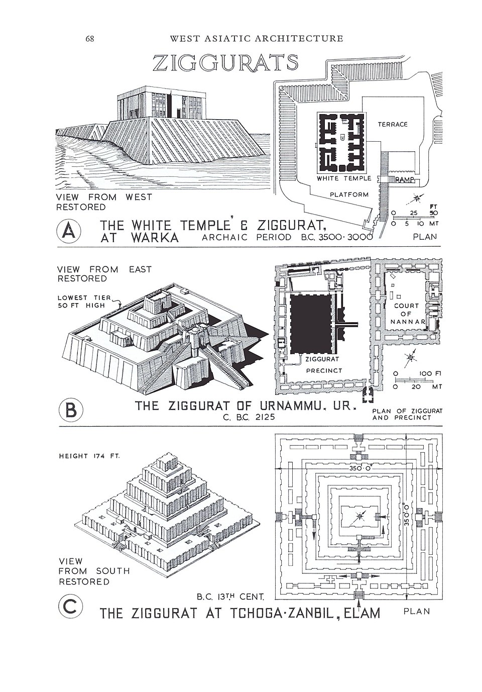
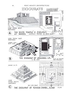
Zeichnungen und Pläne von Zikkurats
PERIOD B.C. 3500-3000 TERRACE WHITE TEMPLE RAMP PLATFORM PLAN FT 50 25 10 MT VIEW FROM EAST RESTORED LOWEST TIER 50 FT HIGH COURT OF NANNAR ZIGGURAT PRECINCT 100 FT 20 MT PLAN OF ZIGGURAT AND PRECINCT B THE ZIGGURAT OF URNAMMU, UR, C. B.C. 2125 HEIGHT 174 FT. VIEW FROM SOUTH RESTORED B.C. 13TH CENT. THE
-
Thread
USB-Pegel bei 3,3V?
3.3V Sind es bei Full/Low Speed.. High Speed sind deutlich weniger als 3.3V nämlich ca. 400mV .. Man muss zwischen Spannungsversorgung und Signalpegel Unterschieden! Es gibt auch Chips die 1.8V Versorgung haben und "USB
-
Thread
Halbbrücke schaltet nur mit minimaler überlappung und nicht im Dutycycle
Mosfets. Im Oszillogram sieht man am obersten und untersten Channel die Spannung am Gate. Bei der High-Side ist eine Bootstrap vorhanden die das Potenzial am Gate auf 14,6 V über dem Potenzial an Source anhebt. Bei der Low-Side ist das Potenzial 15V gemessen gegen Ground. Rboot ist an die gleiche
empfehlen, den fließenden Strom zu messen. Der kann ganz anders aussehen als gedacht. Wenn das Gate low ist und der Strom weiterfließt, fließt er durch die Bodydiode. Wenn der gegenüberliegende FET einschaltet, muss erst einmal die Diode geräumt werden. Das kann einen erheblichen ShootThrough-Strom durch
-
Thread
Low Speed CAN fault tolerant TJA1055 Terminierung
systems will have less bus cable lengths compared to bigger networks and thus have no problem with a higher total termination resistances."
Für die, die hier mit 120Ohm Terminieren wollen, dass ist bei Fault Tolerant bzw. auch Low Speed CAN genannt nicht anzuwenden. CAN != CAN Die Terminierung funktioniert hier anders! Die Terminierung ist direkt an der Transceiver Seite mit z.B. 5,6KOhm umgesetzt und nicht wie man es vom HS
-
 Bild
Bild
Sammlung alter technischer Handbücher und Datenbücher
. Wir bauen die Elemente. VALVO WS3 Integrierte programmierbare Logikschaltungen 1983 Datenbuch 58 Low Level Measurements KEITHLEY For Effective Low Current, Low Voltage, and High Impedance Measurements 59 Graphics Suite CorelDRAW 9 Benutzerhandbuch 60 Adobe Photoshop 6.0 Handbuch Adobe

-
Thread
"3-Wege" Latching Power Schaltung
dem die Modi über Tastendruckdauer ausgewählt werden. Bspw.: - Taster >2sek gedrückt: "System" High bzw. Power On - Taster <1Sek gedrückt: "Pin" High - Taster erneut <1Sek gedrückt: "Pin" Low - Taster erneut <2Sek gedrückt: "System" Low, bzw. Power Off
Da du 5V schaltest tut es wohl ein TPS22996H o.ä., der hat 2 Kanäle und ist aus wenn der Eingang low ist, also aus einem ausgeschalteten uC kommt. Der uC kommt an System und ist daher AN in 2 Zuständen. Der Taster überbrückt den PowerDistributionSwitch zu System. Der uC zieht dann mit high an den
-
Thread
Suche Software / Firmware für Quadra Chek 200
das Gerät funktioniert 4-6. CS am Flash wenn es nicht funktioniert Manchmal ist CS auch immer High, dann zählen die Adressleitungen stur von 0x0 - 0xn durch Was mich etwas stutzig macht, Reset und VCC sind im Prinzip die gleichen Signale. Ich hätte gedacht der Reset wird extern erzeugt kommt mit
einen Transistor parallel zum Reset welcher das Singnal nach dem Einschalten ein paar huntert ms auf Low zieht und so den Pushbutton simuliert. Oder einen neuen DS1670, kostet bei Mouser allerdings über 12€. Woran könnte der 1670 denn gestorben sein? Nicht das der 1k PullUp zu klein ist. Intern ist
-
 Bild
Bild
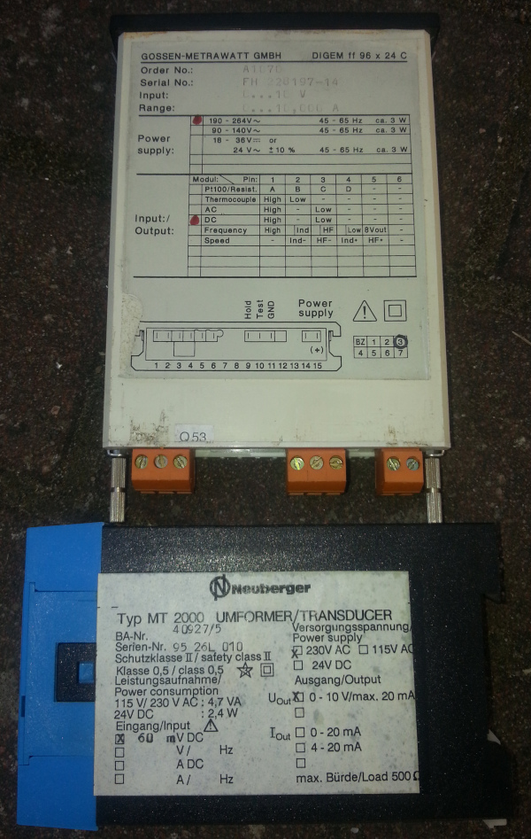
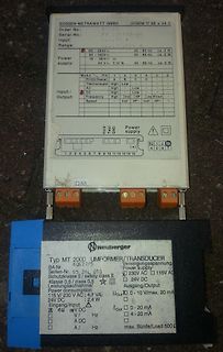
Typenschilder von Gossen-Metrawatt und Neuberger Transducern
Power supply: 16-36V~ 45-65Hz ca. 3W 24V+ ca. 3W Module/Pin/1/2/3/4/5/6 Thermocouple A B C D - AC High Low - DC High Low 8Vout Frequency High Ind HF Low Ind+ HF+ Speed Ind- Ind+ HF+ Hold Test Power Test GND supply 1 2 3 4 5 6 7 8 9 10 11 12 13 14 15 BZ 1 2 3 4 5 6 7 Neuberger Typ MT 2000 UMFORMER/TRANSDUCER
-
Thread
Linearregler sterben
Noch ein Nachtrag: Mark S. schrieb im Beitrag #7876142: > Standard Elko, wohlgemerkt, kein super low-ESR-Typ Besser aber ein low-ESR mit 200 mOhm (lila), als ein "high-ESR" mit 2 Ohm (rot) ;-)
Chance, den falschen ESR zu wählen, siehe: Lothar M. schrieb im Beitrag #7879400: > Besser aber ein low-ESR mit 200 mOhm (lila), als ein "high-ESR" mit 2 > Ohm (rot) ;-) Oder man findet eine passende TVS-Diode, siehe Messung 03.
-
 Bild
Bild
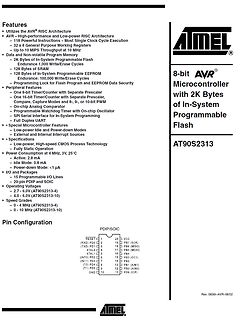
Datenblatt-Auszug AT90S2313 AVR-Mikrocontroller
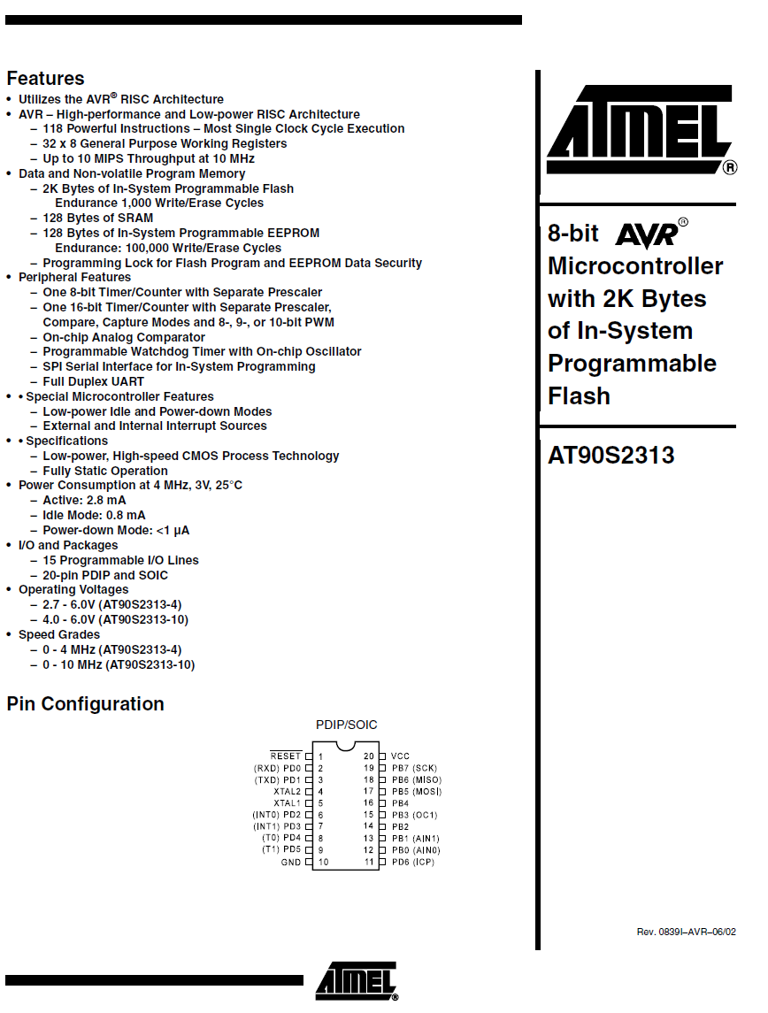
Features Utilizes the AVR RISC Architecture AVR - High-performance and Low-power RISC Architecture - 118 Powerful Instructions - Most Single Clock Cycle Execution - 32 x 8 General Purpose Working Registers - Up to 10 MIPS Throughout at 10 MHz Data and Non-volatile
-
 Bild
Bild
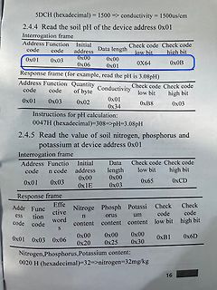
Dokumentation eines Kommunikationsprotokolls für Bodenparameter
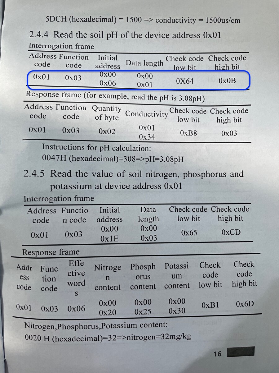
frame Address code 0x01 Function code 0x03 Initial address 0x00 0x06 Data length 0x00 0x01 Check code low bit 0x64 Check code high bit 0x0B Response frame (for example, read the pH is 3.08pH) Address code 0x01 Function code 0x03 Quantity of byte 0x02 Conductivity 0x01 0x34 Check code low bit 0xB8 Check
-
Thread
Benutzt jemand den Delock 64268 Konverter?
unsymmetrisch? Wenn das kein Messfehler ist, klingt das nach der TX/RX-Automatik-"Sparschaltung": High-Pegel über die Bias-Widerstände, nur Low-Pegel aktiv getrieben. Würde mich aber wundern, weil mit dem FT232 solche Hacks unnötig sind. Wie sehen die Spannungen gegen GND aus? Bauform B. schrieb
-
Thread
Fragen zum Sleep Mode
auslöst. Am einfachsten also sicher, indem du den internen Pullup benutzt und den Pin mit dem Taster auf Low ziehst. Du musst dann aber auch in der ISR gucken, dass du ihn abschaltest und erst nach einer Wartezeit wieder aktiviert, und nachdem der Pin wieder "high" ist.
high" war. Ansonsten rennt deine ISR einfach nur Kreise, solange der low-Pegel anliegt.
-
 Bild
Bild
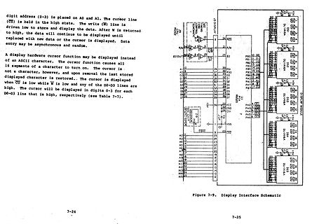
Display Interface Schematic
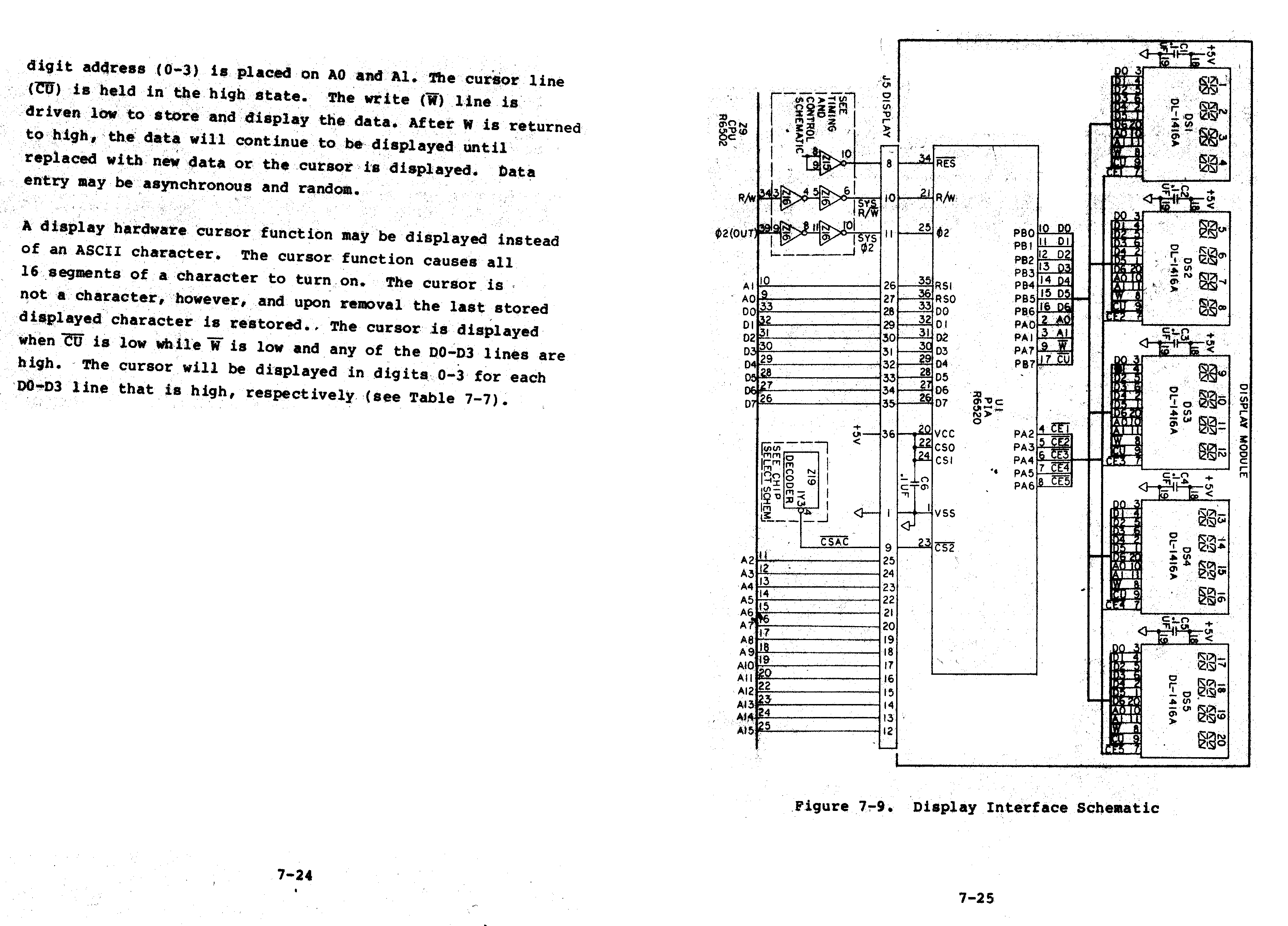
digit address (0-3) is placed on A0 and A1. The cursor line (CU) is held in the high state. The write (W) line is driven low to store and display the data. After W is returned to high, the data will continue to be displayed until replaced with new data or the cursor is displayed. Data
-
Thread
Drohnen-Innovation, Raspberry Pi OS-Update und Python in Hardware
as low as ±0.5ppm. • Superior performance and dynamic stability under airflow and thermal shock. • Multiple Output Enable pins to turn on and off clock outputs for system power optimization and
Mechanical Systems (MEMS) switch. It utilizes Menlo’s Ideal Switch technology to provide an ultra-low on-resistance, metal-on-metal contact to eliminate wasted power. The MM9200 is a high-power SPST micro-electromechanical relay that is smaller, more efficient and has higher performance than equivalent
-
 Bild
Bild
Werbebanner für MEMS-Plattform von ideal switch
ideal switch MEMS platform for power applications Seamless adaptation from milliwatts to megawatts. High power handling Low power consumption Tiny, fast and silent High reliability

-
 Bild
Bild
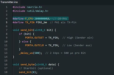
C-Quellcode für einen Bit-Transmitter
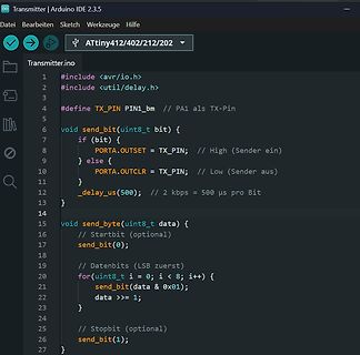
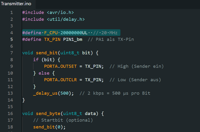
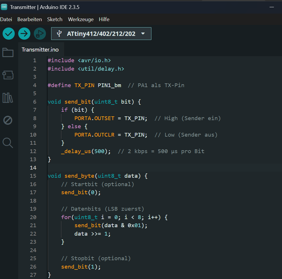
TX_PIN PIN1_bm // PA1 als TX-Pin void send_bit(uint8_t bit) { if (bit) { PORTA.OUTSET = TX_PIN; // High (Sender ein) } else { PORTA.OUTCLR = TX_PIN; // Low (Sender aus) } _delay_us(500); // 2 kbps = 500 us pro Bit } void send_byte(uint8_t data) { // Startbit (optional) send_bit(0);
-
 Bild
Bild
Arduino IDE C++ Code für Transmitter
TX_PIN PIN1_bm // PA1 als TX-Pin void send_bit(uint8_t bit) { if (bit) { PORTA.OUTSET = TX_PIN; // High (Sender ein) } else { PORTA.OUTCLR = TX_PIN; // Low (Sender aus) } _delay_us(500); // 2 kbps = 500 µs pro Bit } void send_byte(uint8_t data) { // Startbit (optional) send_bit(0); // Datenbits (LSB zuerst