RAM AT91SAM9X. ARM926-Kern mit zwei CAN controllern kein onboard flash 32k RAM aber DDR2 support AT91SAM3A. Cortex M3-Kern mit zwei CAN controllern bis zu 512k flash und 96k RAM AT91SAM3X. Cortex M3-Kern mit zwei CAN controllern bis zu 512k flash und 96k RAM Luminary Micro Stellaris LM3S8xxx. ARM Cortex-M3 bis 64kByte RAM und 256kByte Flash CAN und Ethernet Microchip PIC18Fxx8 PIC18Fxx8x. Mikrocontroller mit CAN Schnittstelle Herstellerseite Mitsubishi / Renesas R8C / M16C / M32C. R8C
attachment/691841/4.png) Bildquelle: https://www.instagram.com/p/DViTJ6DFMmz/?igsh=MXFnYnA0bXdzY2x4Nw%3D%3D ### Teledyne e2v Perciva™ 5D – Rückkehr des Kinect for Business Microsoft’s Kinect wurde einige Zeit auch in einer Business-Variante angeboten, die den Tiefenscanner in für professionellere
combines four RH850 CPU cores operating at up to 320 MHz (including two lockstep cores), with up to 8 MB of on-chip flash memory. Developers currently using RH850/P1x or RH850/F1x devices can smoothly transition to the new MCU to meet the requirements of the latest E/E architectures. . . . The RH850
significantly below the 29 MHz peak, wheras the other preamps maintain relatively flat responses between 8 - 30 MHz[/code] Hier der direkte Link (hoffe, er funktioniert): https://lh3.googleusercontent.com/sitesv/AA5AbUBvFP4VWM_dObQqX1JabYH3ZA04vwBQOKJjjt9gD8dZ8xdlltsVROoZ-Paz4VC4pLWcwEqK7P-sK370ruiKuxc3pagVd7mvmxjj1NNEgsRTc5sXkTDVk9
Oder alles: https://drive.google.com/file/d/1iSsCVMf3OHZnzMIGeOVt3Q-_P-8oBD33/view
under development. Characteristics and specifications are subject to change without notice. QN8027 8 PACKAGE DESCRIPTION 10-Lead plastic package – 3x3 mm Body [MSOP] Figure 5: MSOP10 Package Outline Dimensions Millimeters Symbol Description Minimum Nominal Maximum A Overall package height 0.820 0.95
Steigerung zum RGB-Kabel offen halten ;-) Wer's nachbauen will, hier die Bauteile von Digikey. 12xL, 47uH, 0603, 490-LQM18DN470M70LCT-ND 12xC, 22pF, 0603, 478-KGM15ACG1H220JTCT-ND 12xR, 6k8, 0603, 311-6.80KHRCT-ND Kommentare zu den Bildern Boot.jpg Schatten deutlich vermindert, mehr Bildschärfe
Messung mit Funktionsgenerator Delay_Line_ohne_Dämpfung.png Messung mit Funktionsgenerator Delay3.png Schaltplan, LTSpice FBAS_YIN.png C1(gelb) FBAS Signal, C2(blau) Yin (Pin 8) SotB1.jpg Text sehr unscharf SotB2.jpg Schatten am linken Bildschirmrand und den rechten Kanten der roten Buchstaben
level between sync pulses must be between 1.7 V and 8.2 V, see Figure 9(e). 3.0 2)The voltage level for the sync tips must be between +0.9 Vand–0.5V,topreventsubstrateleakageintheIC, 8.2Max see Figure 9(e). (e) 1.7Min Sync 3)The width of the sync pulse
S B _ P E 2 W O P O E P R P I N S C # V W V V L V I [ O S [ E _ [ # # # G C P E C C ] R K ] L D ] [ [ [ N _ W G C S / 1 / / 7 A / ] ] ] G D R 4 4 4 4 4 4 4 4 4 3 3 3 8 7 6 5 4 3 2 1 0 9 8 7 AMBER[2] / SPI_MOSI
e b c 2 1 1 | 1 I a L M s i e 8 s B e d t Z m n o e n t e f - - t Cd >>s b CÖu -Hx Xi Wt *ü J t/1 ,H rH C •H o c M XI h i> $) *—' [0 U >> <H üP O) W ca •a N ryj r-H HD XI T3 -P od 0 r-l O oO X) W EI 15
i f “B” “B” “B” O “F” “F” “F” a M “E” “E” Solder pot 7 “A” Closed “E” “A” Th.023oles “A” .038 x .150 3 end (0,58) (0,97 x 3,81) 0 Dia. min. Inside Dia. x Deep 8 (not a thru hole) 4 , Figure1 Figure2 Figure3 A , c i n “D” “D” r “D” F “C”
FYO 010 INH PPIJLSE 012 Cl—I 01 013 vcOOuT Cl —2 5 FYI 014 RXI 014100 C1 1 1MHz RX2 CD4060 S T 1 ( X ) - ZENER Rege isp, ref f ST2 II 1C3 12 9 01 I 02 RESET,: : 0 0 n 03 Pt V 04 ST3 05 5T7 +5V bis +15V 06 f out 07 C5 + c C 7 1 c 08 09 010 SIB OCn lOOn 011 k e r jk e r Ik e r 012 Bud 2: Schaltbild der
und einen Temperatursensor hat man auch noch. Regen: Ecowitt und Finger melden sich, Temperatur > 3°C Schnee: nur der Finger meldet sich, Temperatur < 3°C Achtung: der Ecowitt darf nicht beheizt sein!
Frank E. schrieb im Beitrag #8012764: > Ein T. schrieb im Beitrag #8012751: >> Frank E. schrieb: >>> Rob R. schrieb: >>>> In so einem Falle ist die KI (kleine Kamera, deren Bilder eine >>>> trainierte KI
8085, 3Y PA2 ETC. 1B 2B 3BSEL1A 2A 3A MC680X 8255 PA3 OR O E ED5B 8 4 B2 B1 (MODE 1) MCS650X P V D D PA4 MC6820 O N 71C03 1 O E ED 5 8 4 B2 B1 U D 2 PA5 P V D D PA4 RUN/ D 3 PA6 O N 71C03 1 HOLD STROBE D 4 PA7
VIN = 5 V, VCC = 5 V, LED FORWARD VOLTAGE = 3.5 VIN= 1 MF, AMB = 25°C UNLESS OTHERWISE SPECIFIED.) 25 1.4 ) ) A 20 ( 1.2 ( D T O E 15 H 1.0 −40°C R E U R 25°C C T E 10 E 0.8 85°C B L A A E 5 N 0.6 E 0 0.4 0 1 2 3 4 5 3.0 3.5 4.0 4.5 5.0 5.5 ENABLE
Ferrite beads/120200mAMHz GND 3 7 R7 1KRST VDDA 3.3V Analog voltage 5V 4 8 3.3V MCU1A C23 C24 CON4-X2 10uF 0.1uF PA0 34 PA0 PE0 141 PE0 PA1 35 142 PE1 MCU1B GND R8 1. The purpose of the 1K resistor here is to provide current limiting
AND CLOCK CHAIN 8 x 8 BiPORT SRAM ARRAY 32,768 Hz CRYSTAL A0-A12 POWER DQ0-DQ7 8184 x 8 SRAM ARRAY LITHIUM CELL E1 VOLTAGE SENSE E2 AND V PFD SWITCHING W CIRCUITRY G VCC VSS AI01377C Doc ID 2412 Rev 8 7/33 Operation modes
lieferte folgende Zusatzinformation: [c] Not to point out the obvious, with the one titled “Samtec HSEC8-DP,” the DP stands for a differential pair design. You’ll notice there are sets of two pins of the same height (for the differential pair signaling), with one short pin on either side (for grounding
steht ein Time-of-Flight-Tiefenscannermodul zur Verfügung, dass eine „variable“ Auflösung zwischen 8 x 8 und 48 x 32 Pixeln bietet. 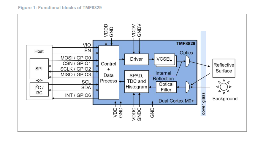 Bildquelle: ams OSRAM Hervorzuheben ist außerdem, dass das Design des Sensors besonders robust gegen „Verschmutzungen“ des Deckglases
packages to help you get the most out of this unique family of Tolerance MP9100 ±1% Standard. 0.40 Ω 3.30 Ω 20.0 Ω 56.0 Ω power resistors. The thermal design issues are the same where power handling 0.050 Ω 0.50 Ω 4.00 Ω 25.0 Ω 75.0 Ω capability is based on the case temperature which is maintained in your design. 0.075 Ω 0.75 Ω 5.00 Ω 27.0 Ω 100 Ω 0.10 Ω 1.00 Ω 7.50 Ω 30.0 Ω 0.15 Ω 1.50 Ω 8.00 Ω 33.0 Ω MP915 TO-126StylePowerPackage 0.20 Ω 2.00 Ω 10.0 Ω 40.0 Ω 0.30 Ω 3.00 Ω 15.0 Ω 50.0 Ω • 15Wattsat +25°C CaseTemperature, deratedtozeroat +150°C. 0.33 Ω • ExposedCeramicHeatDissipatingMountingSurface
begegnet, wo man ein weiteres Passwort vergeben > könnte. https://www.telekom.de/hilfe/apps-dienste/e-mail/programm-passwort-verwalten?samChecked=true
Soul E. schrieb im Beitrag #8005537: > Aua. Ja, SMS kennen nur 8 bit ASCII. Sobald da ein Sonderzeichen oder > Smiley dabei ist, wird eine MMS verschickt Ne, MMS werden komplett anders übermittelt. Das
Number* Package Top Marking MP6528GR QFN-28 (4mmx4mm) See Below * For Tape & Reel, add suffix –Z (e.g. MP6528GR–Z) TOP MARKING MPS: MPS prefix Y: Year code WW: Week code MP6528: Part number LLLLLL: Lot number PACKAGE REFERENCE TOP VIEW F P L D R E U D N T C S F N N G D O n n E G 8 7 6 5 4 3 2 2 2 2
Features Sensitive Layer Over a 0.8 µm CMOS Array Image Zone: 0.4 x 14 mm = 0.02" x 0.55" Image Array: 8 x 280 = 2240 pixels Pixel Pitch: 50 µm x 50 µm = 500 dpi Pixel Clock: up to 2 MHz Enabling up to 1780 Frames per Second Die Size:
probe tested on wafer at Tamb= +25°C Parameter Test Level Min Typ Max Unit Resolution IV 50 µm Size IV 8 x 280 Pixel Yield: number of bad pixels I 5 Bad pixels Equivalent resistance on TPP pin I 20 30 47 6 ® AT77C102B FingerChip 5364A–BIOM–11/03 ® AT77C102B FingerChip . Table 7. 3.3V Power supply The following
linewidth=2, label=key) lines[key] = line ax.set_ylabel(ylabel) ax.legend() ax.grid(True, alpha=0.3) # Format x‑axis as HH:MM:SS on EVERY subplot ax.xaxis.set_major_formatter(mdates.DateFormatter('%H:%M:%S')) # Show x-labels on ALL plots (not just bottom row) ax.tick_params(axis='x', labelbottom=True
Fehlerbehebungen eingefroren. Solche Anwendungen sind jedenfalls mir > noch nicht untergekommen. OK, doch, TeX fällt mir da ein. ;-) Die TeX-Version 3.141592653 ist vom 5. Februar 2021... abwarten. ;-)
arduino espidf+arduinoesp32 in einem Paket. Man muss aufpassen ob das Projekt für arduino-esp32 2.x oder 3.x ist.
common ARINC bus in test and lab environments. To simplify system integration, the HI-85104 supports 1.8 V, 2.5 V, 3.3 V, and 5 V digital I/O, enabling direct interfacing with a wide range of FPGAs and microcontrollers without level shifters. All analog circuitry operates from a single 3.3 V supply, using
Verfügbarkeit eines neuen Windows 11-Images für den Behemoth informiert.  Bildquelle: https://www.instagram.com/p/DT-N1E-lGR5/?igsh=ZWM1eTlhNHM1dnlw ### PX5: Netzwerkstack nun ebenfalls zertifiziert. PX5 ist das „Nachfolgeprojekt“ des einst für ein Azure RTOS verantwortlichen
1 & 2) HP 54603B dc to 60 MHz 3 dB ac coupled, 10 Hz to 60 MHz Rise time 3.5 ns (calculated, HP 54600B & HP 54601B) <2.33 ns (calculated, channels 1 & 2, HP 54602B) <1.4 ns (calculated, channels 3 & 4, HP 54602B) 5.8 ns (calculated
(°C) (µm) with Fiber-Optic Connectors TOTX180 TORX186 Up to 1000 PCF (200/300) TOCP100Q - BTOCP100X - B DC to 8 800 ± 42 5 ± 0.25 – 40 to 85 Up to 800 H PCF(200/230) CF-1071 Series (4) TOTX180 (3) TORX180 (3) Up to 1000 PCF (200/300) TOCP100Q - BTOCP100X - B DC to 6 800 ± 55 5 ± 0.25 – 40 to 85 Up
Andrews McMeel Universal company, 4520 Main Street, Kansas City, Missouri 64111. 04 05 06 07 08 MLT 10 9 8 7 6 5 4 3 2 1 Library of Congress Cataloging-in-Publication Data Adams, Scott, 1957– God’s debris : a thought experiment / Scott Adams. p. cm. ISBN 0-7407-4787-8 1. Philosophy—Miscellanea. 2. God—Miscellanea
4. Pin Configuration: DM9161 LQFP E S B 1 N E [ [ [ [ [ M D D D D D R Y Y Y Y I A C # H H H H M H / R ] P]P ] ] / / L D N N D [ [ [ [ O L S C N D E D D D D D D C C R D M R D R R R R MX X X 6 5 4 3 2 1 0 9 8 7 6 5 3 3 3 3 3 3 3 2 2 2 2
man aus einem vorinstallierten 7-Home ein 7-Professional machen konnte. Hilfreich ist "SLIC_ToolKit_V3.2.rar". Wer es sucht, das saubere hat 344.205 Bytes und die MD5 "da47ab9d2f797d62473cb6ad21bd3b6e". > Angeblich > soll ein Update von Windows 7 auf Windows 10 (und dann auf Windows 11) > nicht mehr
High-efficiency PFM synchronous boost DC/DC converter Ordering Information Product Model QX2304L XX X Packaging TÿSOT23 F: SOT23-5 E: SOT89-3 TOÿTO92 Output voltage 25ÿ2.5V 26: 2.6V … 36:3.6V silkscreen C XX X batch number Output voltage 25ÿ2.5V 26: 2.6V … 36:3.6V QX2304_DS03CN Quancore Electronics Technology
input frequency (see Oscillator). >2. Filter capacitors C1 and C2 must be reduced by a factor of 8 to > maintain the same filter time constants. >3. The output current demanded of pin 8 must be limited to the specified >capability of the LMC567. Ich habe hier nun einige Verständnisschwierigkeiten
noch öfters gezeigt: https://preview.redd.it/gegensprechanlage-ersetzen-v0-zrbxtlwd8eqd1.jpg?width=1080&crop=smart&auto=webp&s=0ad3162a45563e8f31b234301ec85e147accd2b4 https://www.elektrikforen.de/threads/sprechanlage-defekt.25170/ https://www.gutefrage.net/frage/klingel-im-mehrfamilienhaus
TX- 9 7 D D D D 1 M X X X X X XXRXTO RCX X XTXT M C21 C22 8 L L L L I D D D D C CE E L S D D D D C 0.1uF 0.1uF L3 25MHz/49US MAGCOM_HS9024 D _ _ _ _ 2 2R 2 2 2 _ _ _ _ C27 C28 R4 R5 R6 R7 6 5 4 3 O 3 2 1 0 2 3 2 1 0 F.B/120
WITH LCD DISPLAY COMPONENTS SELECTED FOR 200mV FULL SCALE +5V + - -5V IN R1 R 5 C 5 R4 C 1 C2 R2 C 3 R3 C4 DISPLAY C1= 0.1µF 0 9 8 7 6 5 4 3 2 1 0 9 8 7 6 5 4 3 2 1 4 3 3 3 3 3 3 3 3 3 3 2 2 2 2 2 2 2 2 2 C2 = 0.47µF 1 2 3 T I O + F M I O Z F T - 2 3 3 3 D C3= 0.22µF C C C E F L E E O H L A U I V G
E y ∂E ρ system designers face just such a challenge from ∇⋅ E = x + + z = the uncontrolled release of electrical charge into ∂x ∂ y ∂z ε their designs. The most familiar example of For the case of two
3) end of the line to an arbitrary termination voltage RT matches the characteristic impedance of the line, Z .0 adding (1) + (3), i Ir 2V = 1 + Z 0 x V + (R + Z ) x I Z 0 i R T T 0 l T V i I R 2V i (1
Cartman E. schrieb im Beitrag #7986001: > Für solche alten PICs, reicht allemal auch MPLAB 8.92 und XC8 V1.45. Was ist denn der Vorteil einer alten Entwicklungsumgebung?
Gibts auch als PDF für die Knauser: https://raw.githubusercontent.com/TIM168/technical_books/master/C%E8%AF%AD%E8%A8%80/The+C+Standard+Library.pdf Oder den Link verfolge: https://en.wikipedia.org/wiki/C_standard_library Du hast dich mit Deinem "Wissen" ganz schön in eine einsame Nische manövriert
SPACE space Simplified Schematic L1 Efficiency vs Output Current 1.5 µH 100 90 L1 L2 VIN VOUT 80 1.8 V to 5.5 V VIN VOUT 3.3 V 70 ) TPS63020 R1 ( 60 C1 1 0 ▯ C2 c 2×10 µF FB 3×22 µF e 50 R3 i VINA R2 1 0 ▯ E 40 EN 180 N ▯ 30 PS/SYNC V = 1.8 V, V = 2.5 V Power 20 VIN= 3.6 V, VUT= 2.5 V PG Good VIN= 2.4
vs Dimming Duty Cycle 10 LEDs in series Figure 8-3. Efficiency vs Dimming Duty Cycle 100 100 90 90 ) ) ( 80 ( 80 c c n n c c f 70 f 70 E E Vin = 3.0 V Vin = 3.0 V 60 Vin = 3.6 V 60 Vin = 3.6 V Vin = 4.2 V Vin = 4.2 V Vin = 5.0 V Vin = 5.0 V 50 50 0
problem means that if a DMA device writes to a certain memory space, it might not be able to read the same data back. Apple IIe #2: Hardware Protocol for Doing DMA 1 of 9 Apple II Technical Notes H 4 T C 2 A A L D L 7 A O A A H D T D T V D A L N A E T S T S D U O I E B / D C m I V I r D C g L M M i O R D C X c 8 U L l A U A B S I E S a U H O n R I L t - D 7 E S c 0 A ( L P u D M O F ( A T e U R O I B K M C l T 6 R D 5 p A A S A A L G L - 1 A I N A e R I I T ( u T R D U T S N U U i I A K M M C B F B M T I
