-
 Bild
Bild
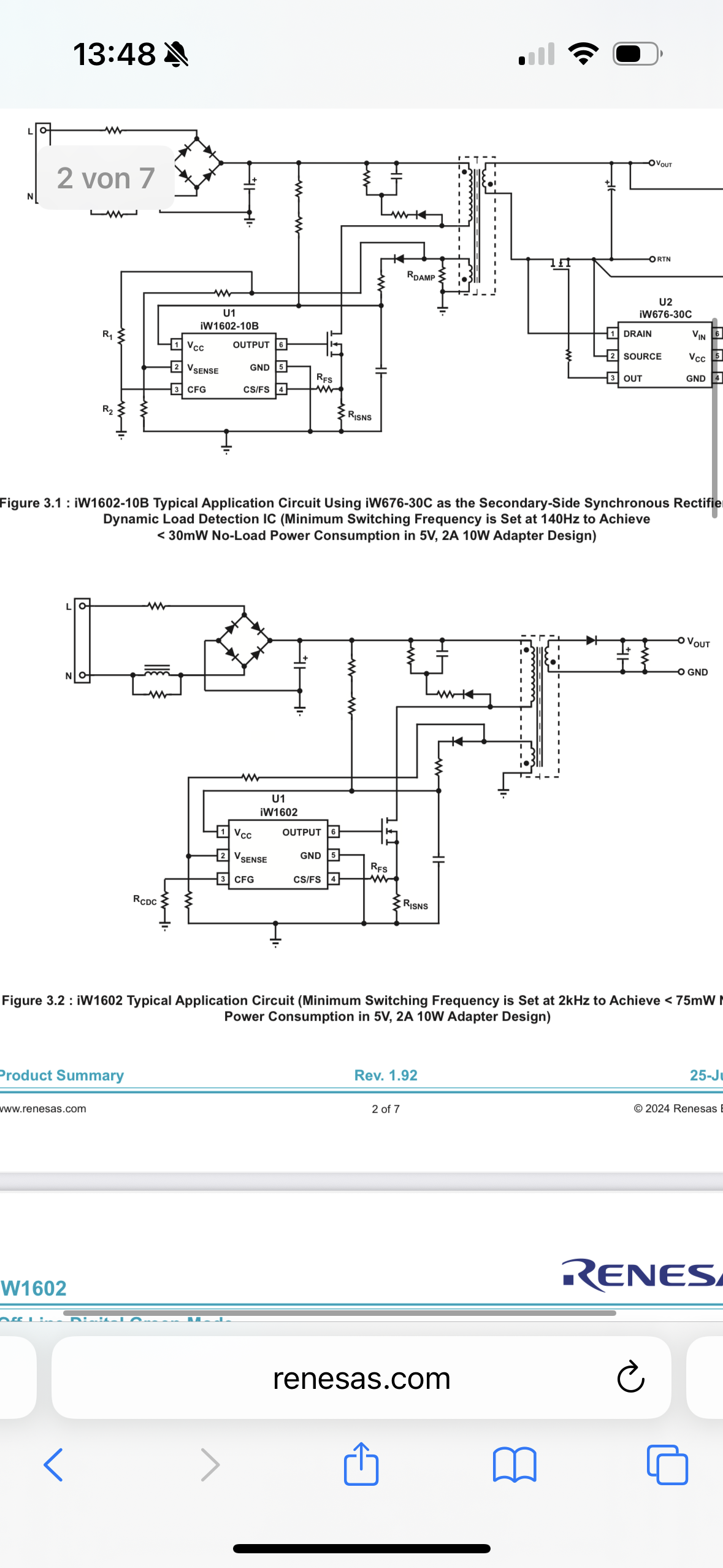
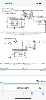
Schaltpläne für iW1602-10B und iW1602 Anwendungen
OUT GND R_ISNS Figure 3.1 : iW1602-10B Typical Application Circuit Using iW676-30C as the Secondary-Side Synchronous Rectifier Dynamic Load Detection IC (Minimum Switching Frequency is Set at 140Hz to Achieve < 30mW No-Load Power Consumption in 5V, 2A 10W Adapter Design Figure 3.2 : iW1602 Typical Application
-
Thread
Strombegrenzung Mosfet Class AB
wusste ich noch garnichts. Heißt das ich kann bei dem IN+ und IN- direkt an den Shunt auf der High Side anschließen? Für meine Anwendung sehr gut das reicht mir. Mal aus reinem Interesse was würde man bei noch höheren Spannungen als beim INA149 erlaubt machen?
-
Thread
Finde den Mosfet
mir mal bitte einen Tipp, wo ich falsch liege. Es sind auf jeden Fall SiRC16DP. Wenn die High-Side schalten, dann eben mit entsprechendem Treiber.
H. H. schrieb im Beitrag #8044524: > > Wenn die High-Side schalten, dann eben mit entsprechendem Treiber. Ok, verstanden. Danke!
-
 Bild
Bild
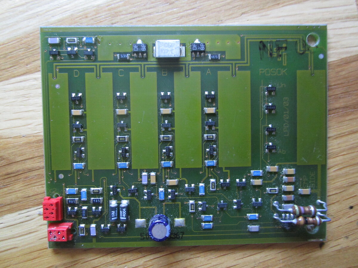
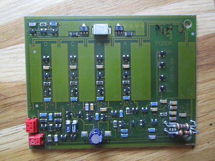
Grüne Leiterplatte mit elektronischen Bauteilen
D C B A POSOK LPD/01/03 SIDE 5667
-
 Bild
Bild
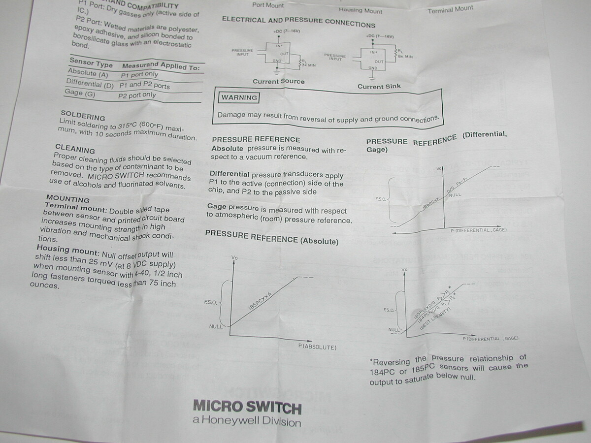
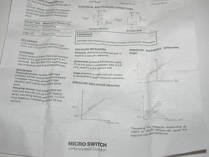
Schaltplan und Diagramme eines Drucksensors
PORT AND COMPATIBILITY P1: Port: Dry gases (only active side of (C.) P2: Port: Wetted materials are polyester, epoxy adhesive, and silicon bonded to a borosilicate glass with an electrostatic bond. ELECTRICAL AND PRESSURE CONNECTIONS PRESSURE INPUT PRESSURE INPUT
-
 Bild
Bild
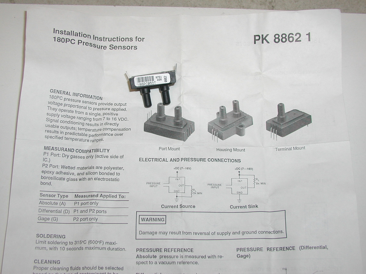
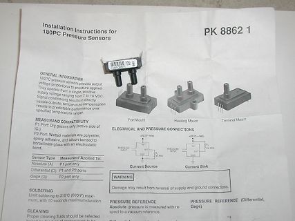
Installationsanleitung für 180PC Drucksensoren
voltage proportional to pressure applied. MEASURAND COMPATIBILITY P1: Port: Dry gases only (active side of I.C.) P2: Port: Wetted materials are polyester, epoxy adhesive, and silicon bonded to borosilicate glass with an electrostatic bond. ELECTRICAL AND PRESSURE CONNECTIONS Sensor Type: Absolute (A),
-
Thread
Sind Kfz Relais weniger belastbar wenn sie Vibrationen ausgesetzt sind?
sollten das aber eigentlich wissen... Ein Ersatz der Relais durch je einen passenden Smart High-Side Power Switch sollte dem nächsten Ausfall vorbeugen. Uwe
Uwe B. schrieb im Beitrag #8043064: > Ein Ersatz der Relais durch je einen passenden Smart High-Side Power > Switch sollte dem nächsten Ausfall vorbeugen. Gibt es auch fertig zum Einstecken in den ISO-(Relais)Sockel: ESR10-NC2A4HB-00-D1-10A von E.T.A https://www.mouser.de/datasheet/3/1143/
-
Thread
3-Transistor Touch → Relais (mit ESD-Schutz) Hilfe
Nimm einen N-Kanal FET oder besser noch so einen Smart Low Side Power Switch. Hier verkauft jemand gerade zufällig den BTS141 im Marktforum. Den normalen PowerFET schützt du wie deinen ersten Transistor. 2 Sensorflächen, eine gegen +, die andere aufs Gate, 10 Megaohm
-
Thread
[V] Smart High-side Power Switch BTS4141N
Ich hätte noch einige BTS4141N Bauform SOT223 Smart Highside Powerswitch: Short circuit protection Overload protection ... uC komnpatible Powerswitch Operating 12-45V / 1,4A 10 Stück: 2,50€
-
Thread
MIC5236 und verpolte Akkus
MIC5236 wird durch einen ohne Enable ersetzt und ein anderer Spannungsregler wird durch einen High Side Switch ersetzt. Dann vertragen alle ICs am Akku -20 Volt, nur die OPs und ein MUX werden durch die Diode geschützt.
-
 Bild
Bild
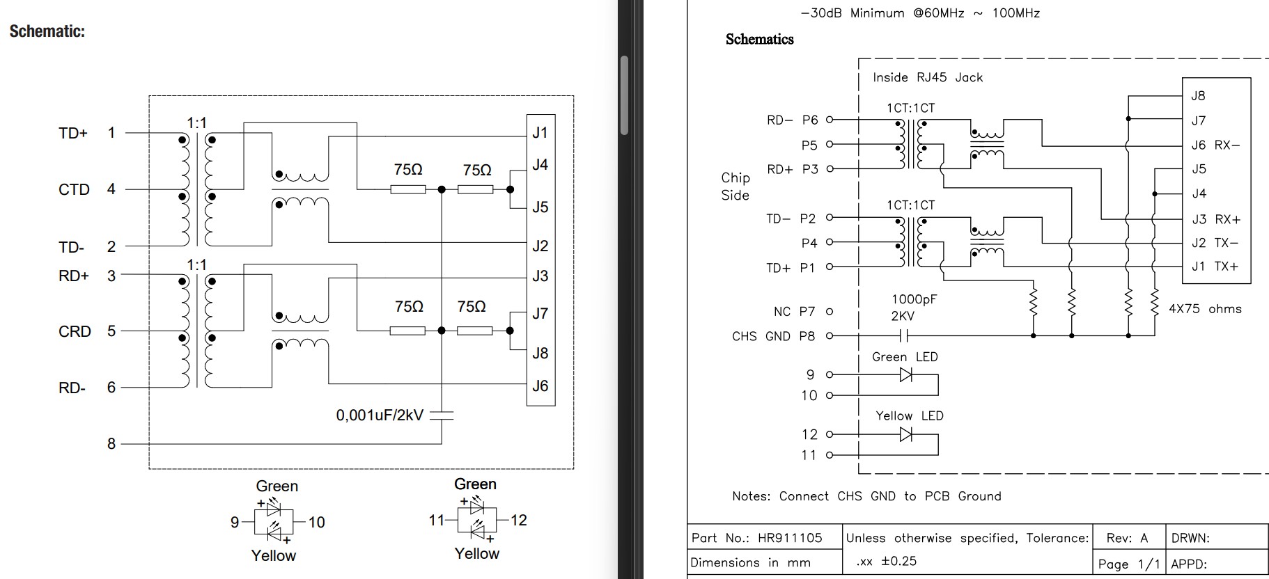
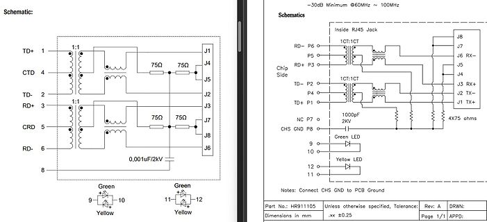
Schaltplan eines RJ45-Netzwerksteckers mit Magnetisierung
@60MHz ~ 100MHz Schematics Inside RJ45 Jack J8 J7 J6 RX- J5 J4 RX+ J3 J2 TX- J1 TX+ 1CT:1CT Chip Side TD- P2 P4 1CT:1CT RD+ P3 RD- P5 P6 NC P7 CHS GND P8 1000pF 2KV 4x75 ohms 75Ω 75Ω Notes: Connect CHS GND to PCB Ground Part No.: HR911105 Tolerance: Rev: A DRWN: Dimensions in mm .xx ±0.25 Page 1/1 APPD
-
Thread
High Side Strommessung
schrieb im Beitrag #8040282: >>> Zu wenig Infos. >>> z.B. gewünschte Bandbreite, Höhe des high side Spannung, etc.
funktioniert, warum könnte man die > nicht einfach überall einsetzen? Warum nicht auch an der Low-Side? Low Side müsste die ja gar nicht Potentialfrei sein. Das Thema hatten wir schon, dass Messung sehr kleiner Ströme auf Low Side absolutes No-Go sind.
-
 Bild
Bild
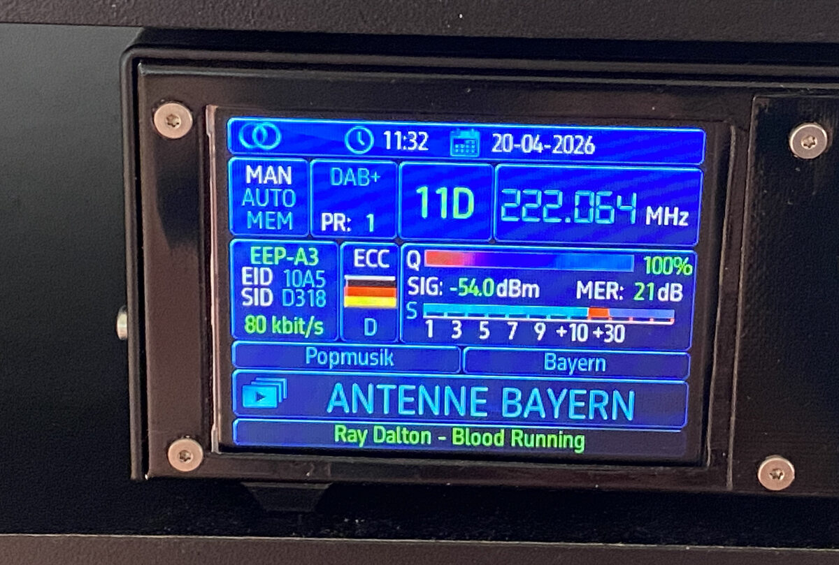
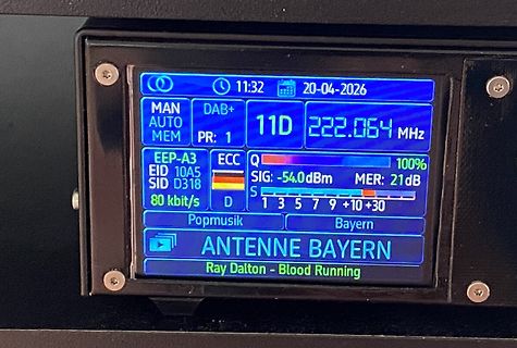
Display eines DAB+ Radioempfängers
32 20-04-2026 MAN DAB+ 11D 222.064 MHz AUTO PR: 1 EEP-A3 ECC Q 100% EID 10A5 SIG -54.0 dBm MER 21dB SID D318 S 1 3 5 7 9 +10 +30 80 kbit/s D Popmusik Bayern ANTENNE BAYERN Ray Dalton - Blood Running
-
 Bild
Bild
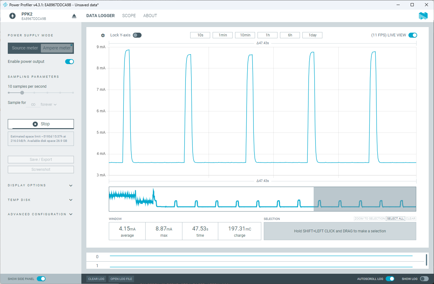
Screenshot eines Stromverbrauch-Messprotokolls
average 8.87mA max 47.53s time 197.31mC charge Hold SHIFT+LEFT CLICK and DRAG to make a selection SHOW SIDE PANEL CLEAR LOG OPEN LOG FILE AUTOSCROLL LOG SHOW LOG

-
 Bild
Bild
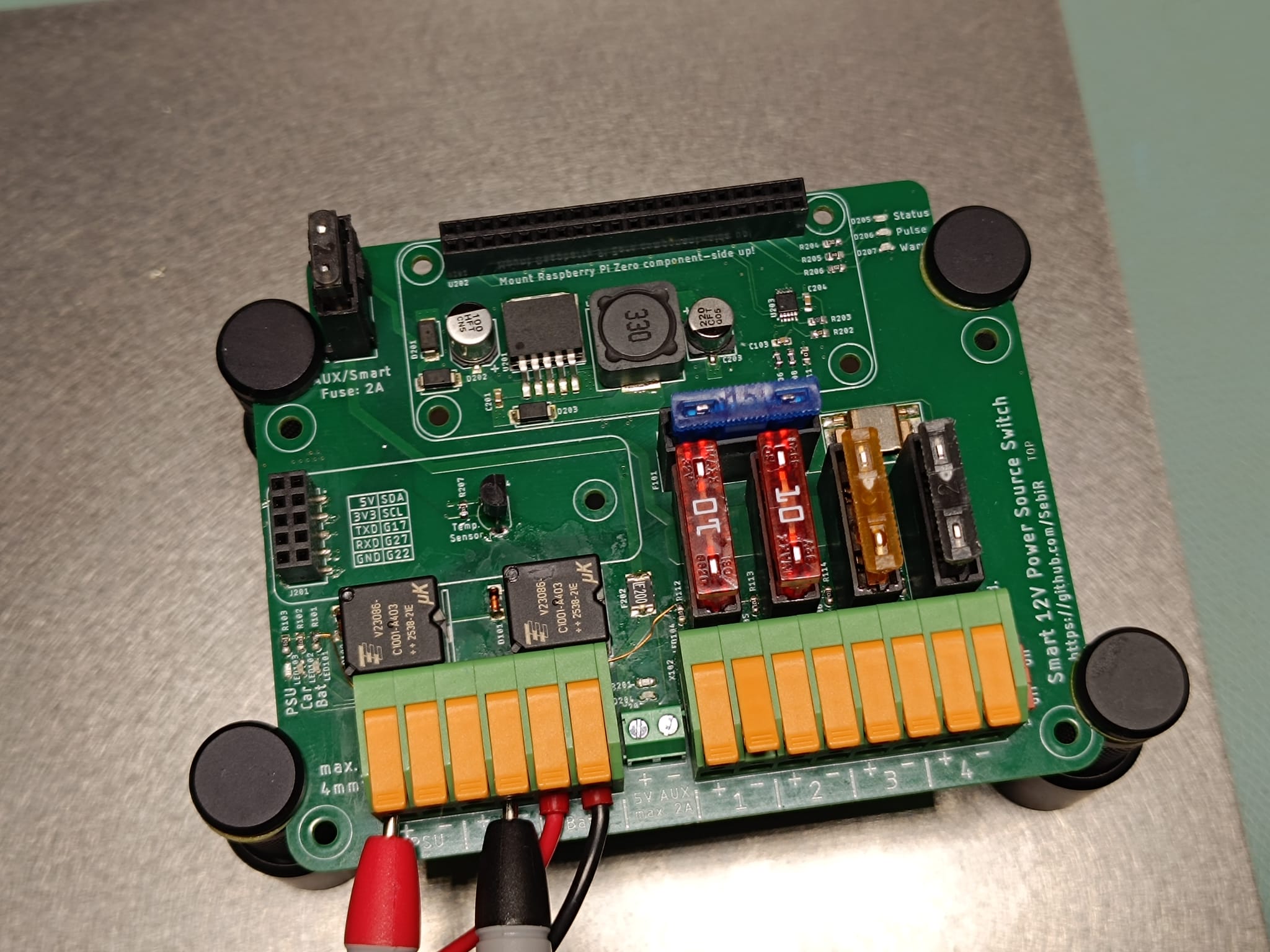
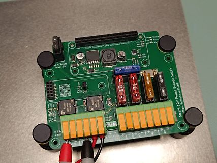
Smart 12V Power Source Switch Platine
Mount raspberry Pi Zero component-side up! Status Pulse War! AUX/Smart Fuse! 2A 330 5V I SDA 3V3 SCL TXD SIO GND G22 2281 C0004-A03 2281C C0006-A03 2281C Smart 12V Power Source Switch https://github.com/Sebh/RIP max. 4mm
-
Thread
PDP8974 Ersatz gesucht
erst ab 8V, bevorzugt mit 12V, also sollte ein normaler MOSFET wie SUP60030E kein Problem sein, high side wird über high side Treiber angesteuert.
kein > Problem sein, Da wird man noch mehr finden, evtl sogar noch besser geeignete. > high side wird über high side Treiber angesteuert. Es gibt nur zwei Low-Side.
-
 Bild
Bild
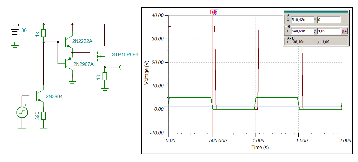
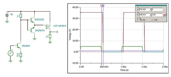
Schaltplan und Oszilloskop-Messkurve
36 1k 2N2222A STP10P6F6 2N2907A 10 2N3904 390 40.00 30.00 20.00 10.00 0.00 -10.00 Voltage (V) 0.00 500.00n 1.00u 1.50u 2.00u Time (s) A x: 510,42n y: 0 B x: 548,61n y: 1,09 A - B x: -38,19n y: -1,09
-
Thread
IGBT Bauteiltester
kann. Der kann das: https://www.peakelec.co.uk/acatalog/dca75-dca-pro-semiconductor-analyser.html#SID=24 Ist aber inzwischen erschreckend teuer geworden.
-
Thread
Pjilips PM2519
N3 5322 216 74066 (532221674066) Seite 100 (95/187) Figure 57 Display p.c.b. lay-out, conductor side: 59 pins keine der Nummern kommt in der KI-Antwort vor. Das PM2534/PM2535 verwendet das L.C.D. 5322 130 90279 (532213090279) https://manualmachine.com/philips/pm2535/4646894-service-manual/ Seite 77/114 8.1 MECHANICAL PARTS Schaltplan Seite 9-2 (89/114) Figure 9.2 Display pcb, component side ST4739 850809 hat 49 Kontaktstreifen, Ansteuerung durch D2101 PCF8576T PEL 5322 209 11129 (Seite 86/114) Das Segment-Layout und die Segment-Zuordnung sieht man auf Seite 9-3 (Seite 90/114).
-
 Bild
Bild
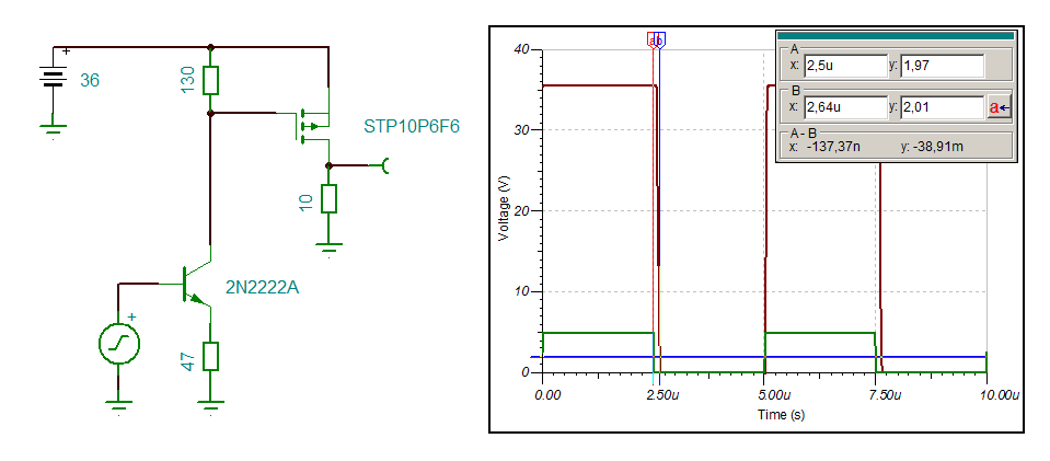
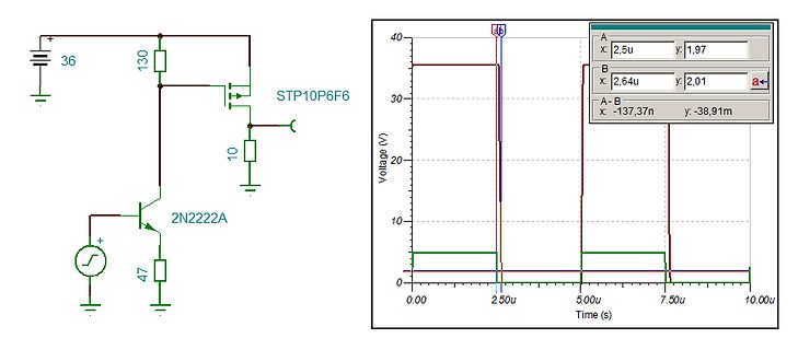
Schaltplan und Oszilloskop-Messkurve
36 130 STP10P6F6 10 2N2222A 47 40 30 20 10 Voltage (V) 0.00 2.50u 5.00u 7.50u 10.00u Time (s) A x: 2,5u y: 1,97 B x: 2,64u y: 2,01 A - B x: -137,37n y: -38,91m
-
 Bild
Bild
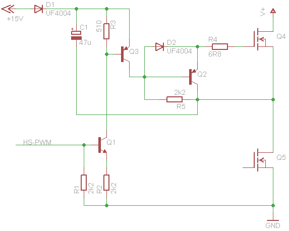
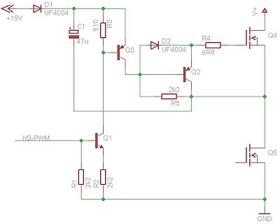
Schaltplan einer Transistorbeschaltung
+15V D1 UF4004 C1 47u R3 510 Q3 D2 UF4004 R4 Q4 V+ Q2 2k2 R5 HS-PWM Q1 R1 2k2 R2 2k2 Q5 GND
-
 Bild
Bild
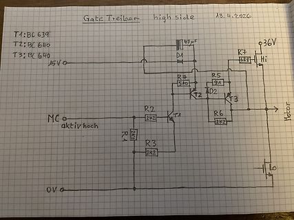
Handgezeichneter Schaltplan eines Gate-Treibers
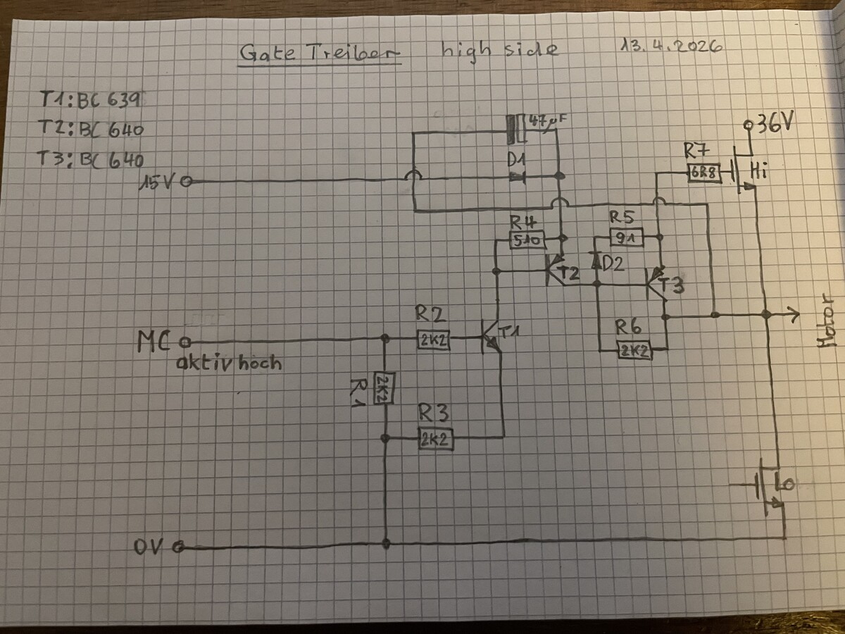
Gate Treiber high side 13.4.2026 T1:BC639 T2:BC640 T3:BC640 15V 47uF 36V R7 688 Hi R4 510 R5 91 D1 D2 T2 T3 MC o aktiv hoch R2 2k2 R6 2k2 T1 R1 2k2 R3 2k2 Motor 0V
-
 Bild
Bild
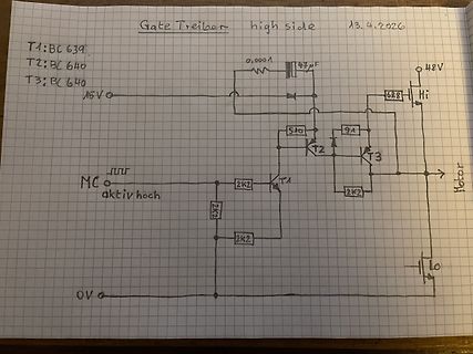
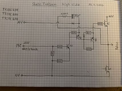
Handgezeichneter Schaltplan einer Gate-Treiber-Schaltung
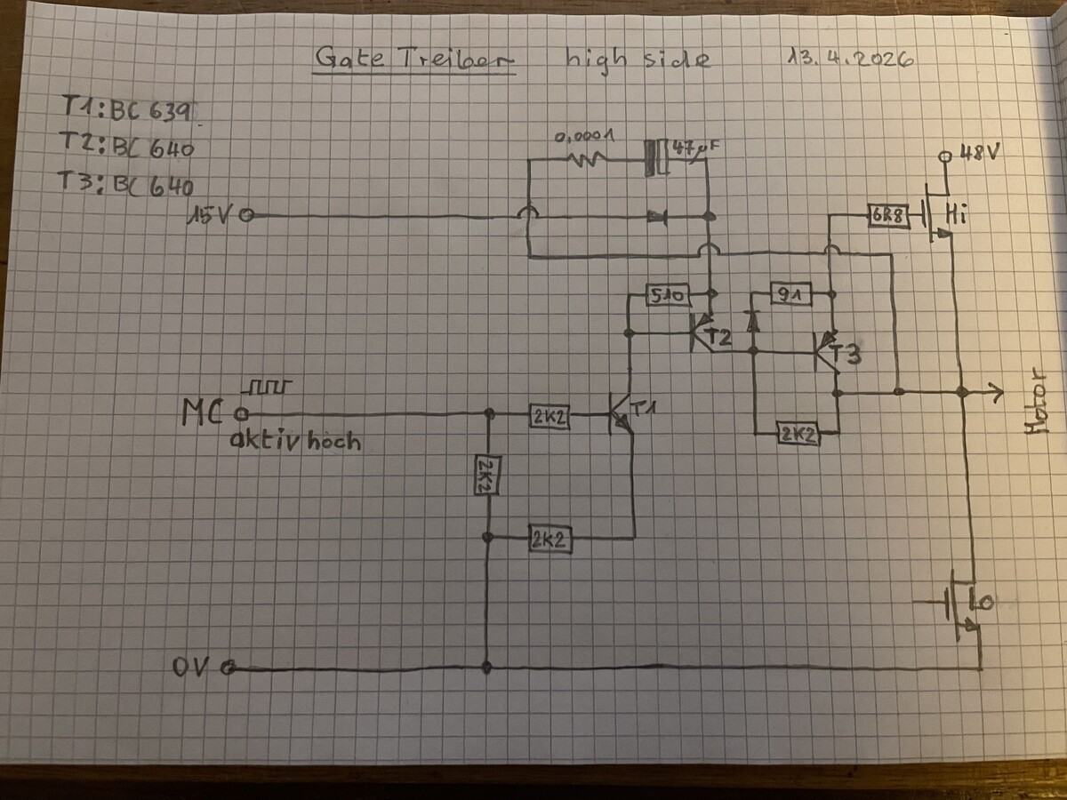
Gate Treiber high side 13.4.2026 T1:BC 639 T2:BC 640 T3:BC 640 15V 0,0001 47uF 48V 68R Hi 510 91 T2 T3 MC aktiv hoch 2K2 T1 2K2 2K2 Motor 0V
-
Thread
Gate Treiber diskret
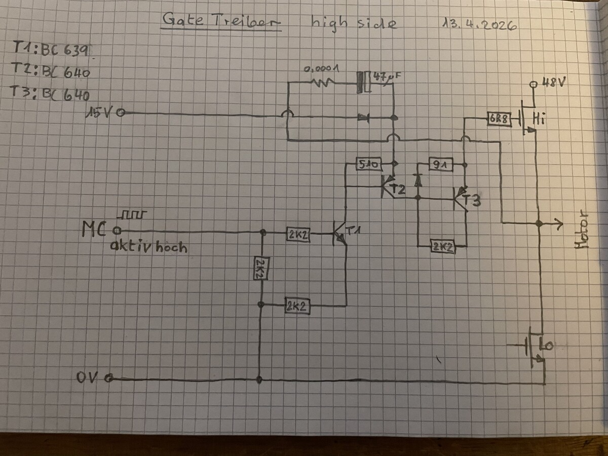
Lothar: Danke für den Kommentar. Ein weiterer Fehler von mir, PWM werde ich natürlich nur bei dem low-side-fet ohne Ladungspumpe anwenden.
ein update. Zur Info: Beim Motorcontroller handelt es sich um einen BLDC, es würde also drei high side Gatetreiber geben und drei low side. Ich hoffe, dass Diode1 den Spitzenstrom beim Aufladen des Elkos verträgt, habe den niederohmigen Widerstand beim Elko entfernt.
-
 Bild
Bild
Handgezeichneter Schaltplan eines Gate-Treibers
Gate Treiber high side 13.4.2026 T1:BC 639 T2:BC 640 T3:BC 640 15V 0,0001 47uF 48V 68R Hi 510 91 MC aktiv hoch 2K2 T1 2K2 2K2 Motor 0V
-
Thread
Neue Bauteile: Verstärker, Drucksensoren und Can-Can
range regulated ICs are unique in having three different feedback modes on the same pin: Primary Side Regulation: where the output is regulated by monitoring the primary side waveform to avoid the need for an optocoupler, Secondary Side Regulation, where the output is regulated by optocoupler feedback
can be supplied within 20 days (MOQ applies). RECOM also offers the RVSxxx range of secondary side rectification solutions including a fully integrated full bridge rectifier IC in a DFN2*2 package, a self-powered external MOSFET rectifier solution that can operate either high side or low side, and
-
Thread
ESD-Schutz für ADC
mal gar nicht ohne. - https://www.st.com/resource/en/application_note/an6249-how-to-protect-a-high-side-current-sensing-against-esd-stmicroelectronics.pdf Und solche Impulse werden nicht mit Widerständen bedämpft (die müssten dann ja diese 6kV aushalten), sondern mit TVS-Dioden, Induktivitäten und
-
Thread
HP nw8540w startet nicht mehr
ist immer noch da. Hinter den beiden Tantals, kommt die fette L3. Danach kommen die switche. N-Side :4395n - Mosfet 16A P-Side :TPCA8030H Der Schluss ist direkt an den Mossfet's. Dann könnte es immer noch der nvidia-Chip sein. Und das könnte immer noch normal sein.
-
Thread
Stromzähler Landis E320 -> MommentanLeistung auslesen
Kapitel 3.1 ein Feld 1.6.0 bzw. 2.6.0 geben. Wenn es nach: https://www.ploesch.de/index.php?side=g-smlerklaert geht, wäre das gesuchte Feld wohl eine 10.7.0 Ich habe allerdings nur die im Bild dargestellten Datensätze. Also eine 60.32.01 und eine 60.01.00 Wie sehr ihr das? .....
-
Thread
P-Kanal MOSFET/JFET - Wo liegt derzeit max. Ugth und min. Rds_on?
Beitrag #8029985: > aber N-Kanal. Das ist mir bekannt. Für die gibt es auch entsprechende High-Side-Treiber und Erzeugung einer Hilfsspannung. Wegen der besseren Beweglichkeit von Elektronen gegenüber Löchern haben n-Kanal-Halbleiter natürlich einen Vorteil. Der Chip fällt daher für gleiche Leistungen
-
 Bild
Bild
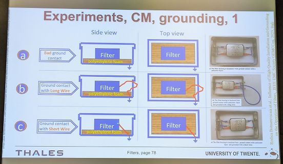
Präsentation von Experimenten zu Filter-Erdung und CM
Experiments, CM, grounding, 1 Side view Top view a Bad ground contact Filter polyethylene foam The filter housing is insulated from ground contact with a polyether layer. b Ground contact with Long Wire Filter polyethylene foam b) The