, damit sie nicht militärisch genutzt werden können. Ein Beispiel: https://portal.u-blox.com/s/question/0D52p0000CIel9sCQB/are-all-ublox-gnss-receivers-able-to-operate-at-altitudes-above-60000-feet-without-modifications-in-the-distant-past-gps-receivers-were-inoperative-above-that-altitude-due-to-dod-concerns
FLARM transponder sind lizenzfrei, billiger und brauchen weniger Energie als Mode-S.
a low voltage S.S.B. amplifier a transformer was required with the following specification: Frequency range: 1.6 − 28 MHz Power handling: 52 W Load impedance: 100 Input impedance: 4.6 The most suitable Ferroxcube material
T 1 SIO, P12[1] 23 P1[3], SWV, TDO ] ] U N F SIO, P12[0] 53 24 P1[4], TDI [ [ X X R OA3OUT, P3[7] 52 25 P1[5], NTRST 1 1 Z Z C C - + - O+1OUT, P3[6] 51 S S , P M M A A A A A 1 1 ] ] + - ] ] I I O O O O 3 I 6 7 [ [ 4 5 6 7 D D D D D [ [ 0 1 2 3 4 ] I D 1 1 1 1 5 5 5 5[ S S D S C C C 1 1 3 3 3 3 3 3 D
that we are guaranteeing the product as “unbreakable.” Code protection is constantly evolving. We at Microchip are committed to continuously improving the code protection features of our products. Attempts to break Microchip’s code protection feature may be a violation of the Digital Millennium Copyright
that we are guaranteeing the product as “unbreakable.” Code protection is constantly evolving. We at Microchip are committed to continuously improving the code protection features of our products. Attempts to break Microchip’s code protection feature may be a violation of the Digital Millennium Copyright
. However, H,L and A registers retain their previous status. 10. If a rising edge is not generated at IP2.0, reset signal occurs every 288 ms at fxx = 455 kHz. To prevent an auto-reset, IP2.0 should be forced low and then high at regular intervals (within 288 ms at fxx = 455 kHz). 5-10 REMOTE CONTROL
S. R. schrieb im Beitrag #4923540: > Nur der Linker kennt die genauen Adressen, es sei denn, du zwingst ihn > (und die Firmware) dazu, dir bereits vorher bekannte Adressen zu > benutzen. Auch
Noch weitere Vorschläge, hat jemand mal so ein Progrämmchen geschrieben? Viele Grüße heiha P.S.: Nochmal, ich bi überwältigt von der Resonanz. Tolle Truppe hier!
zerlegte reinigte und aus den selben Bauteilen wieder zusammensetzte, mit Erfolg. Namaste p.S. habe hier noch SMY 52 mit separatem bulK daraus solte sich eine penthodenäquivalente Feldeffektschaltung bauen lassen.
moduliert, in seiner Amplitude verändert. Dieses Signal geht an den Ausgang des Senders, genannt: *S_ausg*. Drei Signale: S_osz mit 100 MHz S_mod mit 1 MHz S_ausg mit 100 MHz Der prinzipielle Unterschied dieser Signale besteht zwischen S_ausg und den beiden anderen Signalen, S_osz und S_mod
Verknüpfung ausmacht. Durch diese Beeinflussung werden S_osz und S_mod zum S_Senderausgang verknüpft. Was du ganz einfach auf dem Oszi sehen kannst. Beide Periodendauern (Die von S_mod UND die von S_osz) sind im S_Ausgang enthalten. Kurt B. schrieb im Beitrag
S2 10 + Rf/ 3 11 CONVERTER See figure 5 for op amp configuration. S1, S2, S3 should be triple twisted shielded; RH and RL should be twisted shielded; In both cases the shield should be tied to GND at the
https://www.xxxxx.at/build/app.98d70dad.js". en:367:1 Laden fehlgeschlagen für das <script> mit der Quelle "https://www.xxxxx.at/build/ru2ftwofactor.ecdb9b27.js". Domain habe ich unkenntlich gemacht!! Der Browser
Quelle > "https://www.xxxxx.at/build/app.98d70dad.js". en:367:1 > Laden fehlgeschlagen für das <script> mit der Quelle > "https://www.xxxxx.at/build/ru2ftwofactor.ecdb9b27.js". > > Domain habe ich unkenntlich gemacht!! >
"","","","","","","","","","","","",""] (gdb) 14 tbreak main tbreak main Cannot access memory at address 0x800032e &"tbreak main\n" &"Cannot access memory at address 0x800032e\n" 14^error,msg="Cannot access memory at address 0x800032e" (gdb) 15-break-list 15^done,BreakpointTable={nr_rows=
Hallo Phil, wenn's dringend ist: im Land der aufgehenden Sonne hat Nemuisan letzte Woche ein Windows Binary der Version 0.8.0-dev (Build date 2014-03-18) unter https://onedrive.live.com/?cid=36f4d1230f8a673c&id=36F4D1230F8A673C
features both I2C and a Serial interfaces. The serial interface is a standard TTL level UART format at 9600 baud,1 start, 2 stop and no parity bits, and may be connected directly to the serial ports on any microcontroller. Up to 16 SRF02's may be connected together on a single bus, either I2C or Serial
the S1D13700F01 is reset. Turn off the LCD power supplies for at least one frame period after the start of the reset pulse. During the reset period the S1D13700F01 cannot receive commands. Commands to initialize
the S1D13700F01 is reset. Turn off the LCD power supplies for at least one frame period after the start of the reset pulse. During the reset period the S1D13700F01 cannot receive commands. Commands to initialize
the S1D13700F01 is reset. Turn off the LCD power supplies for at least one frame period after the start of the reset pulse. During the reset period the S1D13700F01 cannot receive commands. Commands to initialize
the S1D13700F01 is reset. Turn off the LCD power supplies for at least one frame period after the start of the reset pulse. During the reset period the S1D13700F01 cannot receive commands. Commands to initialize
the S1D13700F01 is reset. Turn off the LCD power supplies for at least one frame period after the start of the reset pulse. During the reset period the S1D13700F01 cannot receive commands. Commands to initialize
Demodulation" aus dem Basisband würde ich nie und nimmer ein SDR System entwerfen. Die Datenrate von dem Mode S Signal ist übrigens 1Mbit/s. D.h. nach dem Demodulator kann ich gemütlich mit 5-10MSamples/s abtasten. Viele Grüße, Martin L.
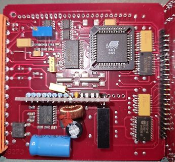
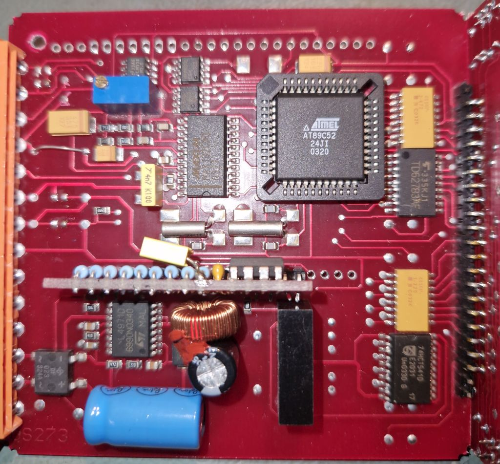
@nepomuk Es ist ein AT89S52 auf der Hauptplatine @wolf17 Wieso mechanisch? 2 Motoren werden mit EINEM Positioner aktuell gesteueert. Es soll ein zweiter Positioner zum ersten synchron laufen. Dabei müssten beide Geräte
dem Leser viel Sucherei ersparen, also z.B. Robert F. schrieb im Beitrag #7995359: > Es ist ein AT89S52 auf der Hauptplatine Robert F. schrieb im Beitrag #7995359: Und bitte bring es auf den Punkt. Wenn du in einem längeren Beitrag auf sieben Leute eingehst, wäre es deutlich übersichtlicher,
tID 40 ms Note 2 6 Interdigit pause reject DO 20 ms Note 2 7 Propagation delay (St to Q) tPQ 8 11 s TOE=V DD 8 O Propagation delay (St to StD) tPStD 12 16 s TOE=V DD U 9 T Output data set up (Q to StD) tQStD 3.4 s TOE=V DD P 10 U Propagation delay (TOE to Q ENABLE) PTE 50 ns load of 10 k , T 50 pF
tID 40 ms Note 2 6 Interdigit pause reject DO 20 ms Note 2 7 Propagation delay (St to Q) tPQ 8 11 s TOE=V DD 8 O Propagation delay (St to StD) tPStD 12 16 s TOE=V DD U 9 T Output data set up (Q to StD) tQStD 3.4 s TOE=V DD P 10 U Propagation delay (TOE to Q ENABLE) PTE 50 ns load of 10 k , T 50 pF
t m l n n r u m n b o o W m C t h C C h s o f s f o C o S S l o H i P P P y i i Z Z Z R i S T E Z Z W T N D A A D A A C D D C D D Figure 29. Timing Diagrams at Data Write The stop transmission command may occur when the card is in different
..........................................20 Rev. G | Page 2 of 20 Data Sheet AD630 SPECIFICATIONS At 25°C and ±VS= ±15 V, unless otherwise noted. Table 1. AD630J/AD630A AD630K/AD630B AD630S Parameter Min Typ Max Min Typ Max Min Typ Max Unit GAIN Open-Loop Gain 90 110 100 120 90 110 dB ±1, ±2 Closed-Loop
100 SNR = 70.3dBc SFDR (2V DIFF) SINAD = 70.2dBc 95 –20 ENOB = 11.4 BITS THD = –86.3dBc 90 SFDR = 89.9dBc ) –40 85 F ) B B 80 ( ( SNR (2V SE) E –60 R 75 D D T S N R 70 G N A –80 S 65 M SNR (2V DIFF) 60 –100 55 SFDR (2V SE) –120 0 50 0 0 6.5 13.0 19.5 26.0 32.5 6 40 45 50 55 60 65 6 FREQUENCY (MHz) 0
3.6 V) CC (V CC = 1.8 to 2.55 V) Item Symbol Min Typ Max Unit Test Condition Serial clock cycle time At write tSCYC 0.5 — 20 s Figure 49 (receive) At read tSCYC 1 — 20 s Figure 49 (send) Serial clock high-level width At write tSCH 230 — — ns Figure 49 (receive) At read tSCH 480 — — ns Figure 49 (send)
refrmaximumV refrespectively,occursatthe lower temperature. Example: maximum V ref= 2496 mV at 30°C, minimum V ref= 2492 mV at 0°C, V ref= 2495 mV at 25°C, ∆T A 70°C for TL431C ǒ 4 mV Ǔ 6 2495 mV 10 a VrefŤ+ [ 23 ppmń°C 70°C Because minimum V occurs at the lower temperature, the coefficient is
SCK tV tHO tDIS HIGH Z HIGH IMPEDANCE SO VALIDOUT tSU tH VALID IN SI 36 Atmel AT45DB081D 3596M–DFLASH–5/10 Atmel AT45DB081D 21.5 Utilizing the Atmel RapidS Function ® ™ To take advantage of the Atmel RapidS function's ability to operate at higher clock frequen- cies, a full clock
H) 70.7 X 38.8 mm Number of dots 128 X 64 dots Dots size(W x H) 0.48 X 0.48 mm Dots pitch(W x H) 0.52 X 0.52 mm 1.2. BLOCK DIAGRAM 3 WWW.TINSHARP.COM TG12864B-03 1.3 MECHANICALSPECIFICATION E . E T D B D T M . N O L P C I R S E A C S H N : S O N T T I R D A N T T D T D C N 性 / L O 特 C E C 组 G 模 N 改 L
magnetic field caused by 82 the ac current. Figure 42 shows the principle of a di/dt current 83 sensor. s 84 e g e 85 ( MAGNETIC FIELD CREATED BY CURRENT S 86 (DIRECTLY PROPORTIONAL TO CURRENT) A H 87 P 88 89 + EMF (ELECTROMOTIVE FORCE) 90 0 0 4 – INDUCED BY CHANGES IN 4 0 MAGNETIC FLUX DENSITY (di/dt) 4
the card is operated): Low bus category classes (26MHz clock with 4bit data bus operation) • 2.4 MB/s Class A • 3.0 MB/s Class B • 4.5 MB/s Class C • 6.0 MB/s Class D • 9.0 MB/s Class E Mid bus category classes (26MHz clock with 8bit data bus or 52MHz clock with 4bit data bus operation): • 12.0 MB/s Class F JEDEC Standard No. JESD84-B42 Page 46 • 15.0 MB/s Class G • 18.0 MB/s Class H • 21.0MB/s Class J High bus category classes (52MHz clock with 8bit data bus operation): • 24.0MB/s Class K • 30.0MB/s Class M • 36.0MB/s Class O • 42.0MB/s Class R • 48.0MB
und damit vom Büro aus per TrovisViewer4 ansprechbar zu machen. Konkret waren die Anschaffung (s.Anhang) ATEN SN3101 - Seriell Console Server https://www.aten.com/global/en/products/kvm/serial-console-server/sn3101/#.W52GMqSbGEc und RJ45 zu DB9 Kabel Natürlich klappt das so -nicht- ootb
Ich empfange über eine RJ12 Buchse am Regler nur 'k's und manchmal ')'
BRIGHT 75 DA0/AN6/P76 PB2 117 BPWRG IN 26.2M> 73.1K> 1 OUT DA1/AN7/P77 PB3 116 IN 1 133 PB4 115 -PM_SLP_S1 134 TXD1/P84 PB5 114 -PM_SLP_S3 IN 26.3M> RXD1/P85 PB6 IN 52.6P> PART NO. W 5 PB7 113 -PM_SLP_S5 IN 52.5P> DESIGNER Y.I 11/20/03 0 1 0 VCC3M 93P4053 _ 1 2 1 S S S S S V CHECKED Y.Y 11/20/03 S 7 V V
MAXIMUM RATINGS (TA= 25°C unless otherwise noted) PARAMETER SYMBOL VALUE UNIT Peak power dissipation at T =25°C, tp=1ms (1) P 1500 W A PK Steady state power dissipation at A =25°C PD 5 W Peak forward surge current, 8.3 ms single half sine-wave I 200 A superimposed on rated load FSM (2) Forward Voltage
and how it decrypts, let alone how to reverse the process and obtain a valid ciphertext key. What's also worrying me at the moment is that there's no 'installed version' for K29 so I have a sinking dread that K29 software may not actually be on the machine unless it's hidden somewhere in an archive

 Bild
Bild