-
Thread
Mindeststrom für Z-Diode
Laständerung stärker sinken darf, kann man die Widerstände auch höher dimensionieren, zB 470k + 100k, gibt 10.56-10.03-9.50 V. Stromentnahme wären 0.5 bzw. 0.1 mA, Verbrauch 30 bzw. 6 mW (statt 0.3mW bei 5µA).
Transistor mit z.B. Uce(max) = 80 V und gut Syromverstärkung. Kommt drauf an, auf was Du Zugriff hast; der BC547C aus der Simuation tuts da nicht.
-
 Bild
Schaltplan eines Solar-Energiezählers
10A Energiezähler BDW B C E Solar 200 Watt 1µ 380 BDW83C R2 E Batterie 6V 6V 7805 100n 100n 1000µ BC 546 2k M LÜFTER 1k Programmieradapter 10k 1k 2,56v 100n Strom Spannung ATmega8-16 10µ Reset DAT gn CL gw 100µ 1MHz rt 8888 8888 8888 Clear Menü Stromsensor AC712 YDJ IT VOM 010629 YDJ IT VOM 10010

-
 Bild
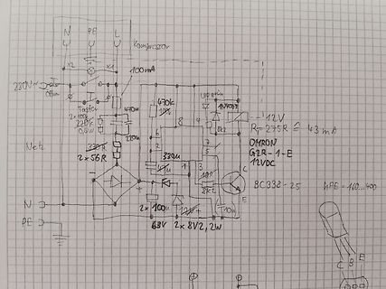
Handgezeichneter Schaltplan eines Netzteils
Kompressor 230V Offner Taster 2x100 220k 0,5W 470k 100k LED grün 1N4007 12V R=275R 43mA OMRON G2R-1-E 12VDC BC338-25 HPE=160...400 330R 2x56R 220u 6u 33u 10k 8k2 8k2 2x100u 63V 2x8V 2,2W N PE C B E
-
 Bild
ESR-Messgerät auf Schaltplan
spannungsführenden Geräten messen! Cx ≥ 1 uF 27kΩ 47kΩ 24kΩ R3, R4, R1, R42 R15, R25 R45 LED, 5mm, rot BZ06-56B IN4146 IN4145 BC546 ...R20 ...R21 ...R31 ...R48 7905 7805 BUZ272 IC1 IC2 IC3 IC4 IC5 ...D1 D2 D8-D11 D12-D15 ...14, 75

-
Thread
8048 Assembler für aktuelle Windows-Versionen
OUTL P1,A 0025 BB04 37 MOV R3,#04 ;SHIFT CTR R3 INITIALIZED TO 4. 0027 BC00 38 MOV R4,#00 ;INITIALIZE DATA REGISTER TO 0. 0029 97 39 NXTB: CLR C ;T0 EXAMINED & T0 CORRESPONDING 002A 262D 40 RDXIN: JNT0 SHIFTD ;DATA
STATEMENT 003E F8 55 MOV A,R0 ;R0 SHIFTED TO R1. 003F A9 56 MOV R1,A 0040 FC 57 MOV A,R4 ;NEW DATA IN R4 SHIFTED TO R0. 0041 A8 58 MOV R0,A 0042 0404 59 JMP START ;JUMP TO
-
Thread
Mikrocontroller.net Design-Update August 2026
Posts 75,52 kB. Lässt sich gut komprimieren, denn da werden dann 695,67 kB HTML draus. Mit ISDN/56k-Modem wären das so 10 Sekunden Däumchendrehen beim Seitenwechseln.
zeigt oder Anhänge, deren Name zufällig passt. Da wären der IRF540, der Transistor 2N3055 oder BC547 und weitere.
-
 Bild
Schaltplan eines LED-Display-Controllers
,Conn_01x02_Pin,UPDI,+5V,Conn_01x06_Pin,IR_Tx,SEG_A bis SEG_G,PA0 bis PA7,U5,AVR6EB32-PI,Q1 bis Q4,BC817,DIGIT_0 bis DIGIT_3,SA56-11,C9,C10,10u,100n,IR_Bx,PWR_FLAG,TSOP48xx,Universal AVRxEB32-I/PT + LED Display Board,Rev. 0.1,Date: 2024-08-03

-
Thread
DDS, Filteranpassung ohne Transformator
Platine mit 4 Buchsen dem TG habe ich 0dB Ausgang verordnet Bild bb - Platine mit Hohlnieten Bild bc - Ein und Ausgangskondensator bestückt Bild bd - alles bis auf die Mittelspulen Bild be - vollständig Bild bf - TG mit -10dB und nur noch bis 400MHz Von ba nach bb, die paar Hohlnieten :)) - ich
der Kombination AD9954 -> 51Ohm gegen AVDD -> Filter -> LMH6552: das 100 MHz Signal liegt bei ca. -56dBm und die Mischpegel auch! und werden nicht größer. Der Weg scheint nicht schlecht - ich kann ihn aber nur über Module beschreiten. Ich habe auch folgendes probiert: AD995X ohne R's -> seriell
-
Thread
Photodiode auslesen für Pulsoximeter
DwYwlgTgBAZgvAIgIwKgFwM6IAwDpsEECsqYIiSeATAVQOx0DM2AHFQGwCcndqIARoiLZUAB0EJhqAG4QhqALaYhAUwC0SFAD4AUFCjAA5lAAeidgBYoRTlSiX7rVPAQiA9Lv3Bpp81Zt2Dhac7M4UoVAA7i4iUAoAhibS8h56BpG+CA4BUEhULNa2YcgIqV4+Zsj5hXZ5BcERLkgR0TiKickIjLiMpZ4GFYg09QRQw1CMjI3hqK0lsHIINLEJSTi4SHTsDOxcRFQh7FOcqPxg8ViuG3TChHf3VKSLt+79wBmVDki29lRW349YG0ygZ4pl6HYpgVGPsJuwWMUEXF4vI4mA2lBDCjkPc+mlgGDKhYWNgJth-OxScwLMUTsjUQp0a5UFiKLiQaBwXQ7H8qVMxhZYjE
-
 Bild
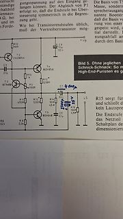
Ausschnitt eines Schaltplans
von Masse, sondern ge- speist wird, a- l darstellt. nungsabfall an- durch den Basis T 2 2N205A R16 56R C5 27p T3 BC546B R10 1k P2 250R R11 470R R13 0,33R R14 10R T5 BDV64B C6 0,1µ R8 2,2k R9 2,2k C7 4000µ 2200V 63V 2200V 25V LS R15 150R 4,5W Die Endstufe das Netzteil Schaltplan de dimensioniert
-
 Bild
Schaltplan einer Lichtsensor-Schaltung mit Monoflop-Ausgang
Metallgehäuse, lichtdicht 100 nF 1.5 MΩ 2n3904 + 9V 56 kΩ BPW34 Sensor 10 MΩ PN4117A oder BF245 100 µF 15 nF 1.5 MΩ 1 kΩ 10 kΩ 10 nF LM 358 100 nF OUT zum Monoflop LED 2n3904 PN4117A E B C Drain Source Gate BPW34 A K + 12V speaker 220 µF BD137 1k 10k 100

-
 Bild
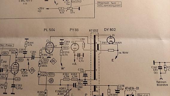
Ausschnitt eines elektronischen Schaltplans
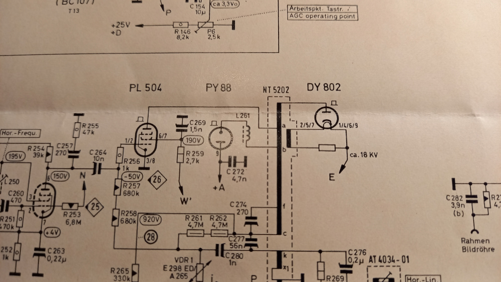
(BC107) T13 +25V D R 146 8,2k P6 2,5k C 154 10u AGC operating point PL 504 PY 88 NT 5202 DY 802 R 255 47k C 257 270 C 264 10n R 256 3/8 6/7 1/4/6/9 R 259 2,7k L 261 C 272 4,7n ca. 18 KV E R 257 680k -50V 26 C 260 470 R 251 10k R 252 1k 253 6,8M 263 0,22u 28 261 R 262 4,7k 265 330k 274 270 277 56n 276 0,2u 280 1n R 269 AT 4034-01 Hor.-Lin.
-
Thread
CRC Berechnung wie die Funktion aufrufen?
0x68, 0x78, 0xB8, 0xB9, 0x79, 0xBB, 0x7B, 0x7A, 0xBA, 0xBE, 0x7E, 0x7F, 0xBF, 0x7D, 0xBD, 0xBC, 0x7C, 0xB4, 0x74, 0x75, 0xB5, 0x77, 0xB7, 0xB6, 0x76, 0x72, 0xB2, 0xB3, 0x73, 0xB1, 0x71, 0x70, 0xB0, 0x50, 0x90, 0x91, 0x51, 0x93, 0x53, 0x52, 0x92, 0x96, 0x56, 0x57, 0x97, 0x55,
-
Thread
Cariad SE Erfahrungen Gesperrt
tesla-byd-und-co-bedrohen-bis-zu-1-5-millionen-jobs-bei-europas-autobauern-a-69cc2c1e-809c-4b18-a6e8-ed8bc0ec2735
autoindustrie/audi-gernot-doellner-will-die-modelloffensive-entschlacken-das-ist-sein-plan-a-bead301e-56e1-4ab1-96ff-5df68123acef
-
Thread
Problem Codesegment
.DB 0x78, 0xB8, 0xB9, 0x79, 0xBB, 0x7B, 0x7A, 0xBA .DB 0xBE, 0x7E, 0x7F, 0xBF, 0x7D, 0xBD, 0xBC, 0x7C .DB 0xB4, 0x74, 0x75, 0xB5, 0x77, 0xB7, 0xB6, 0x76 .DB 0x72, 0xB2, 0xB3, 0x73, 0xB1, 0x71, 0x70, 0xB0 .DB 0x50, 0x90, 0x91, 0x51, 0x93, 0x53, 0x52, 0x92 .DB 0x96, 0x56, 0x57, 0x97,
-
Thread
Neue Bauteile: innovative Schrauben, Mikrocontroller-Thyristoren uvam
der B43693/B43793-Klasse zufrieden. Die sonstigen Parameter präsentieren sich folgendermaßen: [c] 56 µF to 650 µF capacitance Up to +140°C operating temperature [/c] Kommt man mit einem Spannungsbereich von „nur“ 25 V bis 63 V ans Ziel, so empfehlen sich stattdessen die Familien B41687 und B41787
offers a high slew rate of 180V/μs, excellent distortion (spurious-free dynamic range (SFDR) of −100dBc at 1MHz), extremely high common-mode rejection ratio (CMRR) of −100dB, and a low input offset voltage of 3mV maximum under warmed up conditions. [/c]
-
 Bild
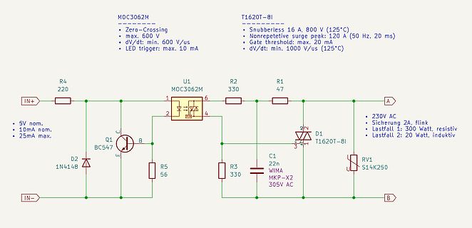
Schaltplan eines Triacs mit Optokoppler
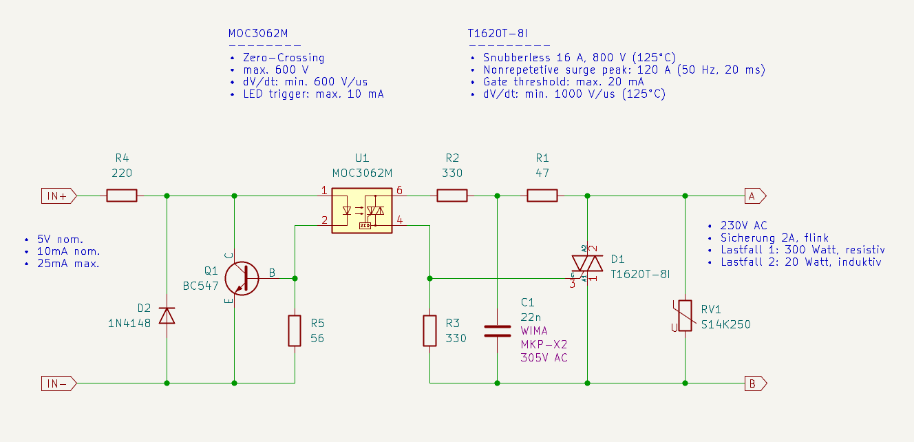
. 1000 V/us (125°C) IN+ R4 220 U1 MOC3062M R2 330 R1 47 A 230V AC 10mA nom. 25mA max. D2 1N4148 Q1 BC547 B R5 56 IN- C1 22n WIMA MKP-X2 305V AC D1 T1620T-8I R3 330 2A flink resistiv Lastfall 1: 300 Watt, resistiv Lastfall 2: 20 Watt, induktiv RV1 S14K250 B
-
Thread
erzeugter Code von ICCAVR ineffizient
ba: 0a c0 rjmp .+20 ; 0xd0 case LED_GREEN_OFF: PORTD |= _BV(LED_GREEN); bc: 94 9a sbi 0x12, 4 ; 18 break; be: 08 c0 rjmp .+16 ; 0xd0 case LED_YELLOW_ON: PORTD &= ~_BV(LED_YELLOW); c0: 95 98 cbi 0x12, 5 ; 18 break; c2
SBI 0x12,0x04 \ 0000002C C007 RJMP ??uart0_rx_isr_6 56 break; 57 case LED_YELLOW_ON: 58 PORTD &= ~BIT(LED_YELLOW); \ ??uart0_rx_isr_2: \ 0000002E 9895 CBI
-
 Bild
Schaltplan eines elektronischen Schaltungsabschnitts
S2 6 5 4 C371 1u C401 3,3n 470 R401 k C409 1u BC173C R411 56k C410 1u R409 1M T401 R407 10k C407 In C372 220u R406 33k R405 5,6k R402 100k C404 47n R403 100k C405 33n R404 4,7k C406 82n R360 100k Bu 303 R413 1k R410 120k R412 2,2k C411 10u TBA 810

-
 Bild
Schaltplan eines Pieps-Sender-Oszillators
Buchreihe Elektronik 170 / 171, 1978 Frech-Verlag, Stuttgart Günter, Wahl Minispione IV, Seite 55 statt BC237 2N3904, Schaltung nicht aufgebaut R5 0.1 R1 12k R2 150k R3 390k R4 12k C1 2.2uF C2 2.2uF Q1 2N3904 Q2 2N3904 Q3 2N3904 Q4 2N3904 R8 56k R11 68k L1 60mH RL1ser 8 K1 L1 L2 0.2 L2 4.8mH RL2ser 2 C3 68nF

-
Thread
Bleiakku Erhaltungsladung, geeignetes Netzteil dafür?
ist das Datenblatt. http://www.st.com/content/ccc/resource/technical/document/datasheet/4b/15/16/56/5e/bc/4a/1d/CD00001634.pdf/files/CD00001634.pdf/jcr:content/translations/en.CD00001634.pdf Teilweise Widersprüchlich und mit Fehler behaftet. Dann baue ich das lieber manuell auf und habe die Möglichkeit
-
 Bild
CrystalDiskInfo S.M.A.R.T. Werte einer Festplatte
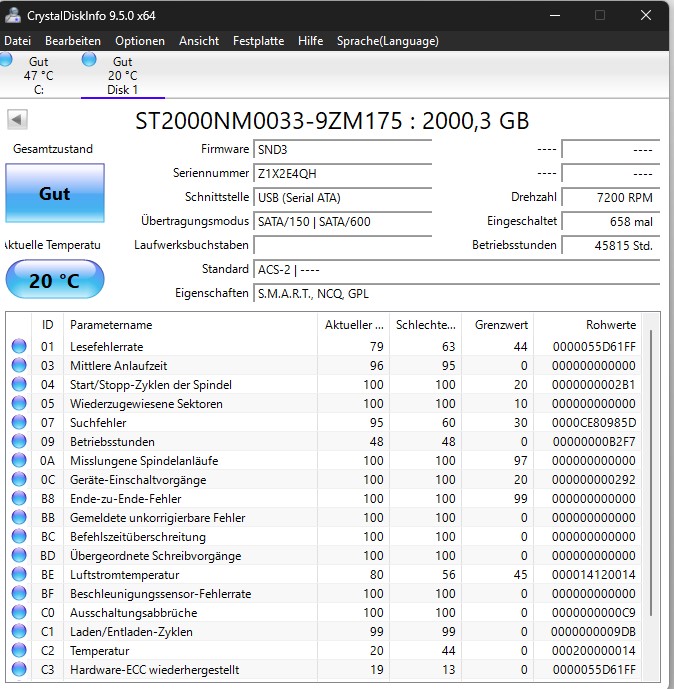
Ende-zu-Ende-Fehler 100 100 99 000000000000 BB Gemeldete unkorrigierbare Fehler 100 100 0 000000000000 BC Befehlszeitüberschreitung 100 100 0 000000000000 BD Übergeordnete Schreibvorgänge 100 100 0 000000000000 BF Lufttemperatur 80 56 45 000
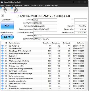
-
 Bild
Präsentation Nuvoton NuMicro M2P481 Power Delivery MCU
MCU System Arm Cortex-M23 core Runs up to 24 MHz 32 KB Flash Memory, 4 KB SRAM Power Supply: 3.3V ~ 56V High immunity: EFT 4.4 kV, ESD HBM 2 kV Operating temperature: -40°C ~ +105°C PD3.1 Support USB PD 3.1 Standard Power Range (SPR) and Extended Power Range (EPR) mode 48V specification, including Programing Power Supply (PPS), Adjustable Voltage Supply (AVS) Support BC1.2 DCP and UFCS Programmable constant voltage(CV) with 20mV/step Programmable constant current(CC) with 20mA/step Integrated gate drivers for external 3.3V~48V, 5A, VBUS NMOS Protection OTP (Over Temperature

-
 Bild
CrystalDiskInfo S.M.A.R.T. Statusbericht einer Festplatte
B9 Hersteller-spezifisch 100 100 97 000000000000 BB Gemeldete Spindelanläufe 86 86 0 000000000000E BC Befehlszeitüberschreitung 100 99 0 000700F0010 BD Übergeordnete Schreibvorgänge 100 100 0 000000000002 BD Luftstromtemperatur 65 56 40

-
 Bild
LTspice Schaltplan und Wellenform-Simulation
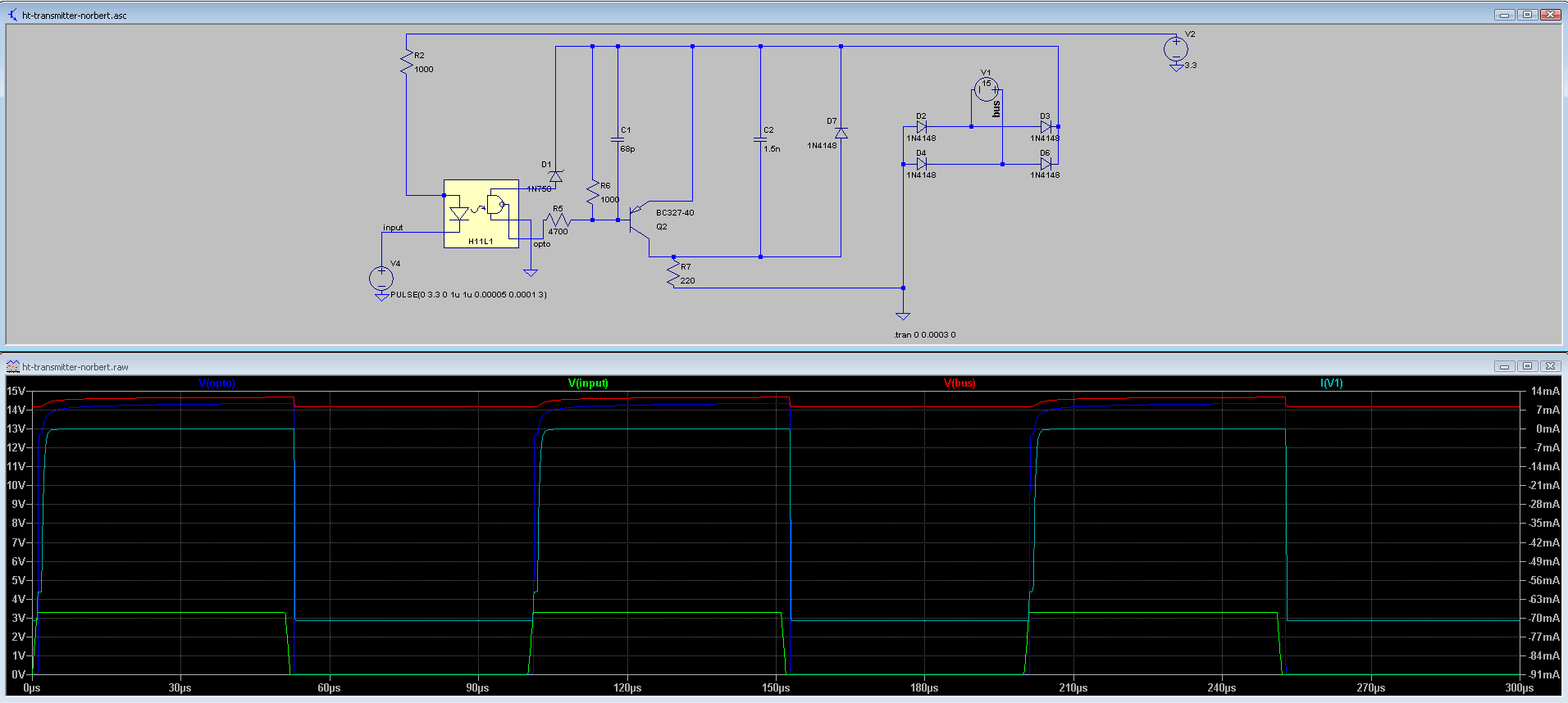
ht-transmitter-norbert.asc R2 1000 C1 68p C2 1.5n D7 1N4148 D2 1N4148 D3 1N4148 D4 1N4148 H11L1 opto R6 1000 Q2 BC327-40 R7 220 V1 3.3 V4 input tran 0 0.0003 0 V(input) V(bus) 15V 14V 13V 12V 11V 10V 9V 8V 7V 6V 5V 4V 3V 2V 1V 0V 30us 60us 90us 120us 150us 180us 210us 240us 270us 300us 14mA 8mA 7mA 14mA 21mA 28mA 35mA 42mA 49mA 56mA 63mA 70mA 84mA 91mA

-
Thread
eActros 600 Update Gesperrt
sprich 1h:47min bei einer mittleren Ladeleistung von 336kW, was einer relativen Ladeleistung von 0,56C entspricht. > ist es schwer, herauszufinden, > wenn du es ernst meinst und wann es ironisch sein soll. Tja, Ironie ist wie Gottseeligkeit und eben auch nicht jedermanss Sache.
product=electricity&source=1&utm_medium=cpc&utm_source=google&utm_campaign=%5Ba:brand%5D%5Bn:search%5D%5Bc:verivox_brand_main%5D%5Bb:cpc%5D&utm_content=e&utm_term=verivox&etcc_med=cpc&etcc_ori=google&etcc_grp=1&etcc_cmp=%5Ba:brand%5D%5Bn:search%5D%5Bc:verivox_brand_main%5D%5Bb:cpc%5D&etcc_par=google&etcc_mty
-
Thread
[C-Code Optimierung] RDM responder
901 10 Data 34 951 11 Data 56 1005 12 Data 78 1054 13 Data 9A 1103 14 Data BC 1151 15 Data
-
 Bild
Technische Zeichnung eines IPROMS-Aufbaus mit Stückliste
IPROM Elektor Dezember 1981 – 12-59 2 Stückliste R1 = 220 Ω R2 = 56 Ω R3 = 1 k R4 = 4k7 R5 = 2k R6 ... R28 = 47 k Kondensatoren: C1 = 4µ/16 V Tantal C2 = 10 n K. Halbleiter: D1 = LED rot 3 mm D2,D3 = DUG T1 = BC547B IC1 = HM6116LP (Hitachi) IC2 = 4071B ausserdem: 24polige