T2 PA A_ SD _S UE E 31 0 0x000000 Reset EFUSE_SYS_DATA_PART2_1 Stores the 1st 32 bits of the 2nd part of system data. (RO) Register 4.90. EFUSE_RD_SYS_PART2_DATA2_REG (0x0164) 2 T2 PA A_ SD _S UE E 31 0
” to “White” (rising time), respectively. The response time interval definition is between 10% and 90% of amplitude. Please refer to the figure as below. % Tf Tr 100 90 Optical White Black White response 10 0 G065VN01 V2 Ver. 1.2 7/24 G065VN01 V2 Note 6: Definition of viewing angle 10, at the screen
AO3400A combines advanced trench MOSFET VDS 30V technology with a low resistance package to provide D (at GS=10V) 5.7A extremely low R . This device is suitable for use as a DS(ON) RDS(ON)(at GS=10V) < 26.5m load switch or in PWM applications. RDS(ON)(at GS = 4.5V) < 32m RDS(ON)(at GS = 2.5V) < 48m SOT23
maximum ratings are stress ratings only. P o Symbol Parameter Min. Max. Unit e r VCC DC Supply Voltage at Pin 20 16 V S OUT Output Current at PG, Fb1, Fb2 Pins 30 mA u p V12, OP1, OP2, FB1, FB2, SS -0.3 16.0 V y VPIN PSON, V33, V5, VREF1, VREF2, OPP, S UVAC, RI, NVP, IN, COMP, PG -0.3 7.0 V u p PD Power
so brauche und fange vorab mit dem an zu basteln, was eben gerade so rumliegt. Macht man aber alles 2x, am Ende. Draht 0.4mm hab ich mir bei reichelt bestellt. https://www.reichelt.at/at/de/shop/produkt/500g_kupferlackdraht_auf_spule_0_40mm-57188 Lässt sich gut löten. Pass auf, dass die Güte
mehr oder weniger Leistung entnimmt. Aus der Modulationsart ergeben sich Nutzsignalfrequenzen von 134.2kHz / 32 (0'en) und 134.2kHz / 64 (1'en) D.h. das Nutzsignal liegt im Bereich von 2kHz bis 4kHz. Aufgrund der Amplitudenmodulation ergeben sich damit Seitenbänder +-4kHz um den 134.2kHz Träger, die man
); //UV: 2.90V Hyst0.2 I2C_8Bit_writeFlag(0x10, 9, 7, 1); //CBEN = 1: Automatic cell balancing on I2C_8Bit_writeToModule(0x10, 0xb, 0b01100010); //EEPROM read-writing /* this is just for test things, dont write
Step-Down sind ebenfalls gut verfügbar. Am gängigsten dürften folgende Module sein: https://shorturl.at/qD4Nn (Amazon: Step Down Buck Converter, DC-DC 3A, 3.2-46V zu 1.25-35V) Bei dem angegebenen Ausgangsstrom von max. 3A bräuchte ich also mindestens 4, lieber 5 solcher Module (60W/(5V*3A) = 4), bei AZ-Delivery
zwar mit der benötigten Leistung. Schau her: https://www.reichelt.de/schaltnetzteil-geschlossen-90-w-5-v-18-a-mw-lrs-100-5-p202973.html?&trstct=pol_15&nbc=1 Da bekommst Du 90W bzw 18A bei 5V raus. Da schließt Du dann Deine LED-Strings an, mit einem ordentlichen Querschnitt von 1.5mm² oder 2.5mm²
Karl B. schrieb im Beitrag #7728103: > Fremdwort für Arduino-Fans. 1: Da irrst du! 2: Die Arduino Welt besteht nicht nur aus AVR und SAM Lothar M. schrieb im Beitrag #7728034: > versuche mal in der aktuellen Arduino IDE-Version 2.3.2 den > Proxy-Port 80 zu setzen. Dann bist du
) Nachfolgende Tabellen zeigen die eingesetzten Baugruppen für die verschiedenen LOGIKEINHEITEN. 4.2.1 Baugruppen-Obersicht TNC355 neue Bardware-Ausführung (farblich gekennzeichnete Anschlußbuchsen) lw 355 m + s m 355 M + s LR355p/w M355C/G U355SN LE355at&~ IZ355svyR 254582 _. 254819.. 254Ba.. 249 516
symmetrische Last vorliegen. Bei kleinem Duty-Cycle wenig Last, bei großem Duty-Cycle eben mehr, bis zu 2 kW. Der eingeprägte Ripple (der PWM Frequenz) sollte eigentlich von der eingangsseitigen Entstördrossel unterdrückt werden. Nun die Frage(n) an jene, die so etwas bereits gemacht haben: ------
Warmwasserspeicher auf Temperatur halten Ist das basteln das Ziel? Wenn nicht: https://www.ta.co.at/news/es-ist-nicht-egal-welchen-pv-heizstab-sie-verwenden https://www.ta.co.at/x2-energiemanagement/aton-power-to-heat
AO3400A combines advanced trench MOSFET VDS 30V technology with a low resistance package to provide D (at GS=10V) 5.7A extremely low R . This device is suitable for use as a DS(ON) RDS(ON)(at GS=10V) < 26.5m load switch or in PWM applications. RDS(ON)(at GS = 4.5V) < 32m RDS(ON)(at GS = 2.5V) < 48m SOT23
voltage protection turned on until the current in the inductor drops to threshold by VOVP pin (Pin2). The external R1 zero. The power MOSFET turn-off time is: and R2 form a resistive voltage divider. T L I LPK (4) Over voltage protection threshold is: OFF V R1 LED V 0.90 (6) OVP R2 Operating
Test conditions The chip supply voltage VDD --- 5.2 --- V --- 0.7* The signal VIH --- --- V VDD input flip VDD=5.0V threshold VIL --- --- 0.3*V V DD The frequency FPWM --- 1.2 --- KHZ --- of PWM Static power IDD --- 1 --- mA --- consumption 5 / 18 Document
CHARACTERISTICS (continued) Efficiency vs Load Current Efficiency vs Load Current Using Vds Sense Ch.2 = 3.3V, Ch.1 = Off Ch.2 = 1.8V, Ch.2 = Off 100 100 V IN24V V = 24V 90 IN 90 VIN 36V 80 VIN 36V % % ( 80 ( 70 C C I I I I 60 F 70 F E E 50 60 40 50 30 0 1 2 3 4 5 0 1 2 3 4 5 6 7 LOAD CURRENT (A) LOAD
ADC2 sets ADC_CTRL1.ENDCIEN, when the conversion of the regular sequence of ADC1 or ADC2 is completed, an ENDC interrupt will be generated. At this time, if ADC_CTRL2.ENDMA is set, a DMA transfer request
dB for Active Filters and Gain Stages Low Offset Voltage: 4.2 mV Maximum Unit Gain Stable Rail-to-Rail Input and Output – Input Voltage Range: -0.3 to +5.2 V at 5V Supply Operating Power Supply: +2.3 V to +5.5 V Operating Temperature Range: −40℃ to +125
Range: -0.2 to +5.2 V at 5V Supply Operating Power Supply: +2.3 V to +5.5 V Operating Temperature Range: −40℃ to +125℃ Applications Photodiode Amplification Sensor Interfaces Audio Outputs Active Filters
Operation at Moderately Heavy Loading. Figure 8. TinySwitch-II Operation at Medium Loading. G 4/05 5 TNY263-268 200 0 3 VEN V - 100 DC-INPUT 8 I P CLOCK 0 10 D MAX V 5 BYPASS 0 IDRAIN 400 200 V DRAIN 0 0 1 2 Time
to the power switches. VCC LD1 VB 6 Q1 CB 7 R1 + HO HV1 5 VS L L R S1 LOAD LOAD IR2110 VCC L D2 VCC + C1 Q2 HV2 R 1 2 LO 2 LS2 COM Figure 5A: Typical Half-Bridge Circuit with Stray Inductances Improve local decoupling. 3a. Increase the bootstrap capacitor (CB) value to above 0.47 µF using at least
modelJulia.jl Friction = Polynomial([0.25, 0.0, 0.1] * 0.001) = Polynomial(0.00025 + 0.0001*x^2) ERROR: LoadError: UndefVarError: Par not defined Stacktrace: [1] top-level scope at /home/christoph/Entwicklung/Modell/modelJulia.jl:15 [2] include(::Module, ::String) at ./Base.jl:377 [3] exec_options
= L*I^2/2.0 Rotorposition 0° W = 1.89mJ ==> L = 3.8mH Rotorposition 90° W = 1.38mJ ==> L = 2.8mH [/code] Diese Werte stimmen gut mit den Messungen von Christoph M. überein. Das ist eher Zufall
MF 2K2 MF 2K2 MF 2K2 MF 2K2 MF SEL_RELAY* 14 G Q6 11 RELAY7 TP164 RELAY7 S1 15 CLR Q7 12 TP165 S0 Y Y Y Y Y Y Y IC 74HC259 A A A A A A A TRIG/RC5 PWM_OUT E E E E E E E TP167 R R R R R R R DGND_SK131 GND1
1.40 1.73 1.88 2.34 2.80 2.98 3.24 3.68 3.76 motor cannot maintain minimum speed at approximately COP in W/W 0.38 0.58 0.66 0.90 1.14 1.25 1.41 1.69 1.75 1,850 rpm). 3 Motor start error (The rotor is blocked or the differential
); //UV: 2.90V Hyst0.2 I2C_8Bit_writeFlag(0x10, 9, 7, 1); //CBEN = 1: Automatic cell balancing on I2C_8Bit_writeToModule(0x10, 0xb, 0b01100010); //EEPROM read-writing /* this is just for test things, dont write
BEA-630 ATX-Netzteil von Bicker vor mir. https://www.bicker.de/bea-630_industrie_pc-netzteil_300w_90-264v_pfc_atx12v_ac-dc_ps2_24-7_62368-1 Dieses hat einfach plötzlich ausgeschaltet und ließ sich nicht mehr einschalten. Ob es dabei ein Knall oder sonstiges Geräusch gegeben hat, kann ich leider nicht
PSU is working fine again! For anyone googling for the references: the board number is 030115HG2, and my PSU is rebranded Emacs HG2-6400P 400W, but is internally exactly identical as your BEA-630. Hope this helps!
); //UV: 2.90V Hyst0.2 I2C_8Bit_writeFlag(0x10, 9, 7, 1); //CBEN = 1: Automatic cell balancing on I2C_8Bit_writeToModule(0x10, 0xb, 0b01100010); //EEPROM read-writing /* this is just for test things, dont write
how-to-burn-boot-loader-of-arduino-uno-r3-usin-aurdino-mega-2650/320626 Library for monochrome displays, v2: https://github.com/olikraus/u8g2 Sample code for using u8g2: https://wokwi.com/projects/376501375827109889 Very good Pinouts for all Arduinos: https://devboards.info/ PWM: https://www.arduino.cc/reference
Mess doch mal mit einem Multimeter die Spannungen an den Pins der Schnittstelle. Meist wird 2,3 und 5 (GND) benutzt. AM PC sollte Pin 3 ca -9V haben. Am Autoadapter sollte Pin2 -9V haben.
Ah ja, siehe hier https://www.obd-2.de/support/faqs/obd-2/53-welches-obd-2-protokoll.html und https://www.flexihub.com/de/oobd2-pinout/ ist ja praktisch, dass da verschiedene Pins zum Einsatz kommen
port pin is set as output. The PWM waveform is generated by setting (or clearing) the OC2x Register at the compare match between OCR2x and TCNT2, and clearing (or setting) the OC2x Register at the timer clock cycle the counter is cleared
CMPS10 module with a wide range of popular controllers. The CMPS10 module requires a power supply at 3.3 - 5v and draws a nominal 25mAof current. There are three ways of getting the bearing from the module. Aserial interface, an I2C interface or a PWM output. Mode selection For data on each mode please click the mode heading. Note the CMPS10 looks at the mode selection pins at power-up only. I2C mode Serial mode PWM mode To enter the I2C mode of operation leave To enter the serial mode of operation To enter the PWM mode of operation the mode pin
run at 5.0 V while the “newer” 400 kHz devices can work at 3.3 V. There could also be more than one master in the bus: 24 2 AN10216-01 I C Manual 2 Parallel to I C Bus Controller I C Hot Swap Bus Buffer 2 PLUG
16MHz at 5V, as measured during production. 6.8.2.6 OSC20 error at 3V Name: OSC20ERR3V Offset: 0x24 Reset: [Oscillator frequency error value] Property: - Bit 7 6 5 4 3 2 1 0 OSC20ERR3V[7:0] Access R R R R R R
register, the vector table contains these three interrupt vectors: 1. The non-maskable interrupts (NMI) at vector address 1. 2. The Priority Level 1 (LVL1) interrupt at vector address 2. 3. All priority level 0 (LVL0) interrupts at vector address 3. This feature is most suitable for devices with limited memory
Heidenreich | copyright Elektor Aus Sicherheitsgründen wird nach dem Boost: on / off (Neu-)Start des PWM-Generators erst Boost-Time: 1 Sek. / 2 Sek. / 5 Sek. dann der Ausgang freigegeben, wenn der PWM-Freq.: 1 kHz / 2 kHz / 5 kHz Betriebswahlschalter vorher auf „aus“ PWM-Step: 1 % / 2 % / 5 % / 10 % stand
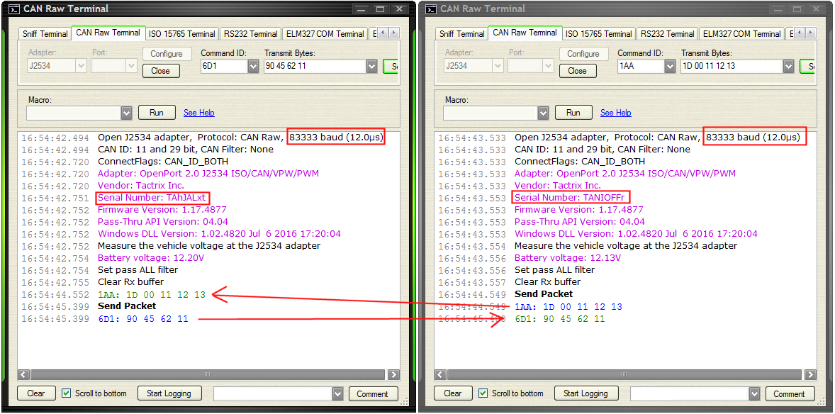
CAN Raw Terminal
Adapter: J2534
Port:
Configure
Close
Command ID: 6D1
Transmit Bytes: 90 45 62 11
Macro:
Run
See Help
Open J2534 adapter, Protocol: CAN Raw, 83333 baud (12.0µs)
CAN ID: 11 and 29 bit, CAN Filter: None
ConnectFlags: CAN_ID_BOTH
Adapter: OpenPort 2.0 J2534 ISO/CAN/VPW/PWM
Vendor
Seitenbandunterdrückung einer SSB-Demodulation aus. > > https://www.mikrocontroller.net/articles/AVR_PWM#Tiefpassfilter-Berechnung > da habe ich mal ein elliptisches Tiefpassfilter vorgerechnet. Ich hatte so ein switched capacitor Filter im Auge. https://www.mouser.de/datasheet/2/609/MAX7400_MAX7407
://www.mouser.de/c/?q=MAX7403ESA%2B und davon braucht man zwei.
Rolladenwickler, bis er sich in > Bewegung setzen muss? Uninteressant. Vielleicht aber ist I/O auf SPI/I2C/UART Basis zu realisieren? Sollen höherfrequente Impulse gezählt/ Tastverhältnisse gemessen/ PWM ausgegeben werden? Schon mal einen DCF77 Empfänger mit Shelly betrieben? Erzähl mal.
-hHHKVOdzajl57ef2i2mG-Mr3DdvXuMG7orildBK5FqvUiJPLzJ4jkGPqd6fAg.htdyULY1XLEF8sCcmEdA-b5woeQeqoxXWhOlceoNEh4&dib_tag=se&keywords=iluminize+remote&qid=1714842881&sprefix=iluminize+remote%2Caps%2C151&sr=8-4 Und zusätzlich
-070WS-C-IPS-46 11. Reliability Test t No. SYMBOL TEST CONDITION REMARK 80℃±2℃ 96H e 1 High Temperature Storage ResPower offt 25℃ e -30℃±2℃ 96H h 2 Low Temperature Storage Restore 2H at 25℃ s 70℃±2℃ 96H a 3 High Temperature Operation Power on t 4 Low Temperature Operation -2Power onH Afelectrical defectsand a 60℃±2℃ should not happen. D 5 High Temperature & Humidity Operation 90%RH 96H -20℃←→25℃←→70℃ y 6 Temperature Cycle 30min 5min 30min a After 10 cycles, restore 2H at 25℃ l 7 Vibration Test 10Hz~150Hz, 100m/

 Bild
Bild