Max B. schrieb im Beitrag #7653884: > Hab mich irgendwie von Al. K. verwirren lassen Ist nicht schlimm, geht Anderen auch so. ;-))) MfG alterknacker
erhältlich), sondern diskret mit Z-Diode und Transistor. Davor hatte ich Türklingeln mit 7 Tönen (2x D195 Schieberegister) und danach 15 Töne D193/ 74154.
latched at the trigger to assist in point placement. There are three decimation modes: normal, min/max, and hires: H Normal (sub-sample) mode throws away samples between saved sample points. H Min/max mode saves the maximum and minimum samples over the decimation interval. H Hires mode gives extra resolution
Semiconductors Product specification NPN power transistors BD135; BD137; BD139 FEATURES PINNING • High current (max. 1.5 A) PIN DESCRIPTION • Low voltage (max. 80 V). 1 emitter 2 collector, connected to metal part of APPLICATIONS mounting surface 3 base • Driver stages in hi-fi amplifiers and television circuits.
Amplifiers 1.4 Quick reference data Table 2. Quick reference data Symbol Parameter Conditions Min Typ Max Unit V collector-emitter voltopen base - - 80 V CEO IC collector current - - 1 A ICM peak collector currentsingle pulsep t ≤ 1 ms - - 1.5 A hFE DC current gain VCE = 2 V;CI = 150 mA 63 - 250 hFEselection
TOM. There are two cases that give a transition without Compare Match. OCR0A changes its value from MAX, like in Figure 14-7. When the OCR0A value is MAX the OCn pin value is the same as the result of a down-counting Compare Match. To ensure symmetry around BOTTOM the OCn value at MAX must correspond
Application n d , GS Rotor Regulator SG-C17xxZ27S 7 R Sele,tSon Guide TJ VZ m m Z 2 7 RPart Number IF(AV)(Max.) Min. Max. e V o V BatteZy 2 SG-C17LXZ27R 35 A Stator R 1 7 V SG-C17VLZ27R 50 A o t - C SG-C177xZ27R SG-C17VVZ27S 60 A 235 °C 24 V 30 V N S G C 1 SG-C17WVZ27S 80 A G - SG-C17WVZ27R S SG-C17xxZ27-DSE
supply rail 4. Quick reference data Table 1. Quick reference data Symbol Parameter Conditions Min Typ Max Unit VDS drain-source voltage 25 °C ≤ T j 175 °C - - 100 V D drain current VGS = 10 V; Tmb = 25 °C; Fig. 2 [1] - - 120 A DM peak drain current pulsed; p ≤ 10 µs; Tmb = 25 °C; Fig. 3 - - 780 A Ptot total
kaufen. Du brauchst halt einen Studenten/Lehrer/Ausbilder der das für Dich macht, dann kostet das Teil 195€. Gut die Lizens läuft dann auf den Namen dessen der sie offiziell gekauft hat, aber solange Du das nicht kommerziell nutzt wird's wohl keinen interessieren. Vielleicht reich ja für's erste die 90
es nicht nur CAD ODER Modelling... Es bedarf beides. Ich bin ca. im Jahr 2001 oder 2000 über 3DS Max in die 3D Geschichte gekommen. Seit 6 Jahren habe ich nun mit dem 3D Druck angefangen. Und betreibe heute obige Farm als kleines Unternehmen nebenher.
Feature Pb Free Solder Process Non-Pb Free Solder Process Average Ramp Up Rate (T to T ) 3°C / second Max. 3°C / Second Max. s p Preheat - Temperature Min (T sin.) 100°C 150°C - Temperature Max (T sax.) 150°C 200°C - Time (tsMin to s Max) 60 to 120 seconds 60 to 120 seconds Time Maintained Above Critical
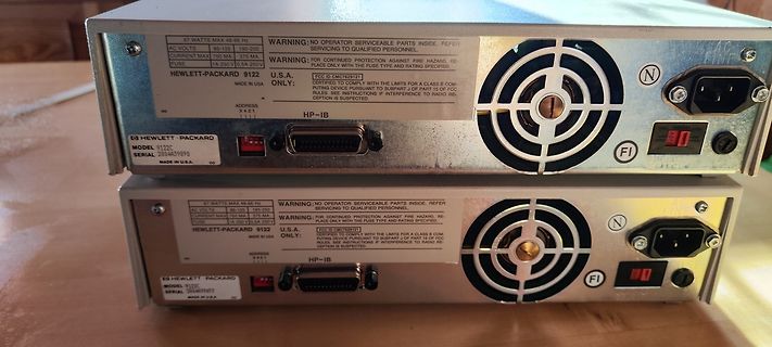
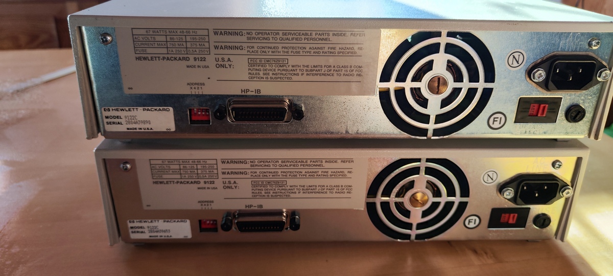
67 WATTS MAX 48-60 HZ
AC VOLTS 195-260
CURRENT MAX 375 MA
FUSE 0.5A 250V
HEWLETT-PACKARD 9122
U.S.A. ONLY:
MADE IN USA
WARNING: NO OPERATOR SERVICEABLE PARTS INSIDE. REFER
SERVICING TO QUALIFIED PERSONNEL.
FCC ID
Microtower Small Form Factor PCI slots 2 Full Length 5V 32 bit PCI slots 2 LP 5V 32 bit PCI slots Max power per slot 25W 25W PCIe x1 slot 1 1 Max power per slot 10W 10W PCIe X16 slot 1 Full Height card 1 LP profile card Max power per slot 75W 25W External Bays 3.5" 1 1 5.25" 2 1 IDE Internal 3.5" HDD
Microtower Small Form Factor PCI slots 2 Full Length 5V 32 bit PCI slots 2 LP 5V 32 bit PCI slots Max power per slot 25W 25W PCIe x1 slot 1 1 Max power per slot 10W 10W PCIe X16 slot 1 Full Height card 1 LP profile card Max power per slot 75W 25W External Bays 3.5" 1 1 5.25" 2 1 IDE Internal 3.5" HDD
Philips Semiconductors Product specification PNP power transistor BD330 FEATURES PINNING • High current (max. 3 A) PIN DESCRIPTION • Low voltage (max. 20 V). 1 emitter 2 collector, connected to metal part of APPLICATIONS mounting surface 3 base • Powerswitchingandamplification,especiallyinportable equipment
Philips Semiconductors Product specification NPN power transistor BD329 FEATURES PINNING • High current (max. 3 A) PIN DESCRIPTION • Low voltage (max. 20 V). 1 emitter 2 collector, connected to metal part of APPLICATIONS mounting surface 3 base • Especially for battery equipped applications. DESCRIPTION handbook
K MAXIMUM MATERIAL CONDITION. 6. STANDARD IS 751−07.ARE OBSOLETE. NEW MILLIMETERS INCHES G DIM MIN MAX MIN MAX A 4.80 5.00 0.189 0.197 C N X 4_ B 3.80 4.00 0.150 0.157 C 1.35 1.75 0.053 0.069 SEATING D 0.33 0.51 0.013 0.020 PLANE G 1.27 BSC 0.050 BSC −Z− H 0.10 0.25 0.004 0.010 0.10 (0.004) M J 0.19
R = 2 kΩ, unless otherwise noted. S L Table 2. 1 AD620A AD620B AD620S Parameter Conditions Min Typ Max Min Typ Max Min Typ Max Unit GAIN G = 1 + (49.4 kΩ/G ) Gain Range 1 10,000 1 10,000 1 10,000 2 Gain Error VOUT= ±10 V G = 1 0.03 0.10 0.01 0.02 0.03 0.10 % G = 10 0.15 0.30 0.10 0.15 0.15 0.30 % G =
großenAuflösung bleibt die dieAlias-Effektevermeidet? Schwankung ohneAuswirkung. A knapp über 2 ⋅ max D DasAbtastergebnis wirdverbessert (Dithering). B knapp über 𝑓 max C knapp unter 𝑓max AF622 Welcher Filtertyp ist geeignet,umAlias- 2 Effekte zuvermeiden,und wo ist das Filter D knapp unter 𝑓 max
Theory of Operation.............................................................................. 195 5.16.2.1 Standard ATA Emulation .......................................................... 195 5.16.2.2 48-Bit LBA Operation............................................................... 195 5.16.3 SATA Swap Bay Support ....................................................................... 195 5.16.4 Hot Plug Operation ............................................................................... 195 5.16.4.1 Low Power Device Presence Detection ....................................... 195
the dutyCycle is changed. int dutyCycleMin = 10; // Minimum dutyCycle (brightest LEDs). int dutyCycleMax = 90; // Maximum dutyCycle (dimmest LEDs). unsigned long msecButton = 0; // Time since the button was pressed unsigned long debounceTime = 350; // Time until a new interrupt is accepted int refreshRate
±VS= ±15 V, unless otherwise noted. Table 1. AD630J/AD630A AD630K/AD630B AD630S Parameter Min Typ Max Min Typ Max Min Typ Max Unit GAIN Open-Loop Gain 90 110 100 120 90 110 dB ±1, ±2 Closed-Loop Gain Error 0.1 0.05 0.1 % Closed-Loop Gain Match 0.1 0.05 0.1 % Closed-Loop Gain Drift 2 2 2 ppm/°C CHANNEL
Solarmodule, eine Batterie und eine Lastseite schalten kann. Die Batterie operiert zw. 20v und max. 29.4v, bei den Solarmodulen liegt die Leerlaufspannung zw. 40&50v und sie liefern max. 600w. Die Last wird max. 450w betragen. Schalten möchte ich die Lasten via IRFB3006 MOSFETS: Drain-Source
Spoe N. schrieb im Beitrag #7544139: > Die Batterie operiert zw. 20v und max. 29.4v, bei den Solarmodulen liegt > die Leerlaufspannung zw. 40&50v und sie liefern max. 600w. > Die Last wird max. 450w betragen. - ca. 22,5A (wenn es auch wirklich ein Ohmscher Verbraucher mit
<Checksum> Instruct the MK2 to act as a remote panel - switch on, input current limit 12A (of 16A max.) using variant 1 (sending potvalue and scale) 07 FF ‘S’ 03 C0 10 01 01 D2 02 FF ‘S’ AC Send single remote panel command - switch on, input current limit 31.5A using variant 2 (sending absolute current
Therefore, as shown in Fig. 7.14, the B6-bridge and CHB inverter’s voltage ripples are at D = 0.5 and V DC,max /2 and V batt,max2, respectively. The maximal peak current ripple on the inductor ∆I is set at 5% of the peak current. L,max Considering the battery maximal current of I batt,max= 36A, the current ripple
HPI_FEATURE: 0x03]: implementation based on CMD12 Background operations support [BKOPS_SUPPORT: 0x01] Max Packet Read Cmd [MAX_PACKED_READS: 0x08] Max Packet Write Cmd [MAX_PACKED_WRITES: 0x08] Data TAG support [DATA_TAG_SUPPORT: 0x01] Data TAG Unit Size [TAG_UNIT_SIZE: 0x00] Tag Resources Size [TAG_RES_SIZE
HPI_FEATURE: 0x03]: implementation based on CMD12 Background operations support [BKOPS_SUPPORT: 0x01] Max Packet Read Cmd [MAX_PACKED_READS: 0x08] Max Packet Write Cmd [MAX_PACKED_WRITES: 0x08] Data TAG support [DATA_TAG_SUPPORT: 0x01] Data TAG Unit Size [TAG_UNIT_SIZE: 0x00] Tag Resources Size [TAG_RES_SIZE
Hörgeräte Hersteller verkauft das Teil zur Übertragung von Audioquellen, wie TV, den die alten Leute mit 195,-Euro bezahlen(müssen). Ich fand zwar zunächst jede Menge Lötvorschriften Kataloge, z.B. ROHM, Vishay die auch footprints zeigen, aber alles größer als (1,6 x 1,1)mm. Früher gab es den IC-Master,
table_size; /* Table size */ UINT64 used_entries; /* Used entries */ UINT64 max_dib; /* Max DIB (Distance to Initial Bucket) */ UINT64 collisions; /* Sum of the DIB of all entries */ } HT_STAT; BOOL HT_GetStat(HASH_TABLE *ht, HT_STAT *sp, HT_HASH
generated when the counter is equal to TOP. If TOP is updated to a value lower than count upon reaching MAX, the counter restarts from BOTTOM. Figure 21-3. Periodic Interrupt Mode MAX and Event) Request TOP CNT BOTTOM TOP changed to CNT set to BOTTOM a value lower than CNT 21.3.3.1.2 Time-Out Check Mode In
voltage 0...16V, 0...32V ▯▯ Output current 3 to 16A On “Sense” mode it is possible to com- leitungen max. 1V pro Leitung kompen- ▯▯ Schools, Universities, Laboratories pensatethevoltagedropontheloadca- siert. Es ist je ein externer Program- bles up to 1V on each cable. miereingang (0...10V) und ein Monitor
Ripple 15/30 63 mA pk-pk Through 4.7µH inductor and 220µF capacitor, others / 3V3 input 5 IES0103 for max 1s 9 IES0105 for max 1s Input Surge 18 VDC IES0112 for max 1s 21 IES0115 for max 1s 30 IES0124 for max 1s Input Current See models and ratings table See Models and Ratings tabl Input Filter Capacitor
current source Typical Power Capability: Type SOP8 DIP8 z PWM with current mode control European (195-265 Vac) 8W 13W z 9v to 38v wide range VCC voltage US (85-265 Vac) 5 W 8W z Fixed 60KHz switching frequency The AP8012 is available in SOP8 and DIP8 z Automatic skip cycle mode in low load condition

 Bild