
-
 Bild
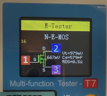
Display eines Transistor-Testers mit Messwerten
M-Tester N-E-MOS 16 D 2 Vt=979mV 1 G 667mV Cg=579pF S 3 RDS=0.5Ω Multi-function Tester - T7
in „H-Brücke mit defektem MOSFET - Bauteil und Ursache bestimmen“ · Analoge Elektronik und Schaltungstechnik · · Fotos
-
 Bild
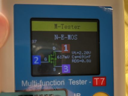
Display eines Multi-Funktions-Testers T7
M-Tester N-E-MOS 37 D 1 Vt=2.20V G 2 617mV Cg=691pF RDS=0.8 S 3 Multi-function Tester - T7
in „H-Brücke mit defektem MOSFET - Bauteil und Ursache bestimmen“ · Analoge Elektronik und Schaltungstechnik · · Fotos
-
PDF
3986pfd.pdf
traces to the MOSFET bridge. ment is determined by the state of the MSx inputs. GL1A, GL1B, GL2A, and GL2B Low-side gate drive outputs for external N-channel MOSFETs. External series MS1 and MS2 These Microstep Select
in „Bitte Hilfe in Englisch“ · Mikrocontroller und Digitale Elektronik ·
-
PDF
3986.pdf
traces to the MOSFET bridge. ment is determined by the state of the MSx inputs. GL1A, GL1B, GL2A, and GL2B Low-side gate drive outputs for external N-channel MOSFETs. External series MS1 and MS2 These Microstep Select
in „Schrittmotorsteuerung“ · Mikrocontroller und Digitale Elektronik ·
-
PDF
AN-1126.pdf
MOSFET; MOSFET causes switching losses and efficiency to suffer. For the MOSFET must be a logic level type that is rated this reason, the MOSFET die must not be oversized, and it must for a suitable RDSn
in „180VDC-Netzteil Ausgangsstrom zu gering“ · Mikrocontroller und Digitale Elektronik ·
-
PDF
1912111437_Dialog-Semiconductor-IW3658-06D_C425003.pdf
sense 2 GND Ground Ground reference 4 HV Analog Internal high voltage MOSFET drain 5 VG Analog Internal high voltage MOSFET gate 6 V CC Power Input Power supply to control logic and MOSFET drive COMP Analog Constant current regulation loop compensation 7 8 CFG Analog OVP level
in „LED Netzteil defekt - Snubber & Chiptyp?“ · Analoge Elektronik und Schaltungstechnik ·
-
PDF
AN101_An_Introduction_to_FETs_70594__VIS.pdf
5b) Circuit Arrangement for N-Channel FET for N-Channel FET Figure 5. Siliconix 3 10-Mar-97 AN101 MOSFETs There are, however, some fundamental performance dif- ferences between MOSFETs and JFETS. JFETs, by na- The metal-oxide-semiconductor FET (MOSFET) depends ture, operate only in the depletion mode.
in „mit 2,7V schalten“ · Mikrocontroller und Digitale Elektronik ·
-
PDF
AN-941_Paralleling_HEXFET_Power_MOSFETs__IR.pdf
941 (v.Int) PARALLELING HEXFET POWER MOSFETs (HEXFET Power MOSFET is the trademark for International Rectifier Power MOSFETs) Summary: • General guidelines • Steady state sharing • Dynamic sharing at turn-on • Dynamic sharing at turn-off • Related
in „300A mit Mosfets schalten.“ · Analoge Elektronik und Schaltungstechnik ·
-
PDF
AN-9010b_MOSFET_Basics__FAI.pdf
November 2,1999 AN9010 MOSFET Basics April 1999 R & D 2 Group Fairchild Korea Semiconductor CONTENTS 1. History of Power MOSFETs...................................................................................................
in „mit 2,7V schalten“ · Mikrocontroller und Digitale Elektronik ·
-
Datei
main.c
BLANK_PORT PORTB #define BLANK (1 << PB0) //@} /** * @name I/O Pins für die Zeilentreiber */ //@{ #define MOSFET_ROW0_DDR DDRD #define MOSFET_ROW0_PORT PORTD #define MOSFET_ROW0 (1 << PD4) #define MOSFET_ROW1_DDR DDRD #define MOSFET_ROW1_PORT PORTD #define MOSFET_ROW1 (1 << PD3) //@} /** * @name Grayscale Data
in „LED-Matrix mit AVR und TLC5940: inaktive LEDs glimmen“ · Mikrocontroller und Digitale Elektronik ·
-
PDF
MIC5158.pdf
the gate of the external MOSFET. 7 D Drain and Current Limit (Input): Connect to external MOSFET drain and ex ternal sense resistor (current limit), or conneand external MOSFET drain (no current limit). DD 8 (3.3V, 5V) S Source (
in „Einstellbarer Linearregler - in etwa so?“ · Analoge Elektronik und Schaltungstechnik ·
-
PDF
TPS40060_TPS40061.pdf
the upper MOSFET. Additionally, there is some delay as the MOSFET gate charges to turn on the upper MOSFET, typically between 20 ns and 50 ns. The higher synchronization must be factored in when programming the PWM
in „Parameter-Berechnung für Schaltregler“ · Analoge Elektronik und Schaltungstechnik ·
-
PDF
FM2112.pdf
以OC , FM2112 系列 IC会自动关闭充电控制用的 MOSFET ( OC 端子),停止充电 ,这个状态称为“过充电状态” 。 过充电状态在如下 2 种情况下可以释放: 不连接充电器时 (1)由于自放电使电池电压降低到过充电释放电压 ( V CR) 以下时 ,过充电状态释放 ,恢复到正常工 作状态 。 (2)连接负载放电 ,放电电流先通过充电控制用 MOSFET 的寄生二极管流过 ,此时,CS端子侦测到一 个 “二极管正向导通压降(Vf)的电压 。当CS端子电压在放电过流检测电压
in „LiFepo4 balancer - China ICs“ · Analoge Elektronik und Schaltungstechnik ·
-
PDF
ISL6545-Renesas.pdf
do not heat the MOSFETs. However, large gate-charge increases the switching removal of a transient load: interval,SW which increases the MOSFET switching losses. t = L x TRAN t = L x TRAN Ensure that both MOSFETs are within
in „Synchronwandler ISL6545A wird heiss“ · Analoge Elektronik und Schaltungstechnik ·
-
PDF
AN-9010.PDF
Oxide the BJT. This application note is a general description Semiconductor Field Effect Transistor (MOSFET). of power MOSFETs and a presentation of some of onsemi’s The power MOSFET is used in applications such product specifications. as Switched Mode Power Supplies (SMPS), computer HISTORY The theory behind
in „SMD Mosfet mit Z-Diode für induktive Last“ · Analoge Elektronik und Schaltungstechnik ·
-
PDF
A200_MCP1407-EP_MIC.pdf
power supplies, the PWM controller may not have the drive capability to directly drive the power MOSFET. A MOSFET driver Input Output like the MCP1406/07 family can be used to provide CL= 2500 pF additional drive current capability. MCP1407 4.2 MOSFET Driver Timing The ability of a MOSFET driver to transition
in „Treiber für IRF1404 ?“ · Mikrocontroller und Digitale Elektronik ·
-
PDF
20002019c.pdf
supplies, the Ceramic PWM controller may not have the drive capability to directly drive the power MOSFET. A MOSFET driver Input Output like the MCP1406/07 family can be used to provide additional drive current capability. CL= 2500 pF MCP1407 4.2 MOSFET Driver Timing The ability of a MOSFET driver to transition
in „Pulsschweisgerät mit Auto Batt Schaltungs Verbesserung“ · Analoge Elektronik und Schaltungstechnik ·
-
PDF
TMC262_datasheet.pdf
MOSFET. The high-side driver supplies VS to the P channel MOSFET gate to close the MOSFET and VHS to open it. The effective low-side gate voltage is roughly 5V; the effective high-side gate voltage is roughly
in „Wärmeentwicklung Mosfet“ · Mikrocontroller und Digitale Elektronik ·
-
PDF
AN1.pdf
High Side MOSFET Gate Drive: The Power of Well Implemented Pulse Transformers Author: Fritz Schlunder SHEF Systems AN-1 Many different techniques and circuits are available for providing high side N-Channel MOSFET
in „Steuerung von Leistungsmosfets“ · Analoge Elektronik und Schaltungstechnik ·
-
PDF
db883bb7785064c5f8a8b3b8f50858ea45a7.pdf
self-contained 1KW 13.56MHz RF source. The module facilitates operation and evaluation of the DEIC420 RF MOSFET gate driver IC and DE275X2-102N06A RF MOSFET in a practical 13.56 MHz RF generator application. It is all-inclusive, pre-tested, and ready to operate. Introduction 4BEADS +15V 1.5K 1/4W D1 C3 + 16V
in „Bauplan für HF Netzteil gesucht.“ · HF, Funk und Felder ·
-
PDF
SC1117DG-PowerIntegrations.pdf
not exceed 1 mA. FB 2 7 S 6 S FEEDBACK (FB) Pin: During normal operation, switching of the power MOSFET is D 4 5 S controlled by this pin. MOSFET switching is disabled when a current greater than 49 µA is delivered into this pin. SOURCE (S) Pin: PI-5553-041910 This pin is the power MOSFET source connection
in „[TIPP] WMF Skyline Vario Wasserkocher“ · Haus & Smart Home ·
-
PDF
CN3795.pdf
the MOSFET as well; many of the logic-level MOSFETs are limited to 30V or less. Selection criteria for the power MOSFET includes the “on” resistance Rds(on), total gate charge Qg, reverse transfer capacitance
in „5V Solarmodul zu 5V USB - Optimierung“ · Analoge Elektronik und Schaltungstechnik ·
-
PDF
CN3795-CONSONANCE.pdf
the MOSFET as well; many of the logic-level MOSFETs are limited to 30V or less. Selection criteria for the power MOSFET includes the “on” resistance Rds(on), total gate charge Qg, reverse transfer capacitance
in „Auseinandergenommene Geräte“ · Analoge Elektronik und Schaltungstechnik ·
-
PDF
CN3795-CONSONANCE.pdf
the MOSFET as well; many of the logic-level MOSFETs are limited to 30V or less. Selection criteria for the power MOSFET includes the “on” resistance Rds(on), total gate charge Qg, reverse transfer capacitance
in „cn3795 Richtige Werte für FB und MPPT“ · Analoge Elektronik und Schaltungstechnik ·
-
PDF
max5056.pdf
19-3348; Rev 1; 9/05 4A, 20ns, Dual MOSFET Drivers General Description Features M A The MAX5054–MAX5057 dual, high-speed MOSFET ♦ 4V to 15V Single Power Supply drivers source and sink up to 4A peak current. These X devices feature a fast 20ns
in „Dual Mosfet Treiber“ · Analoge Elektronik und Schaltungstechnik ·
-
PDF
AND9093-D.PDF
an N-channel MOSFET has several advantages over the additional voltage rail for the gate; the P-channel load switch P-channel MOSFET. For example, the N-channel majority carriers (electrons) have a higher mobility than the does not. As with the N-channel MOSFET, the designer P-channel majority carriers (holes). Because of this, the must ensure that the device maximum ratings and the safe operating area of the P-channel MOSFET are not violated. N-channel transistor
in „Widerstandsdimensionierung im Betrieb als Schalter für RC Elektronik mit IRLIZ44N“ · Analoge Elektronik und Schaltungstechnik ·
-
PDF
CN3722-CONSONANCE.pdf
MOSFET as well; many of the logic level MOSFETs are limited to 30V or less. Selection criteria for theer MOSFET incl udes the “on” resistance Rds(on), total gate charge Qg, reverse transfer capacitance RSS
in „Auswahl Solar-Laderegler für 12V Blei-Akku“ · Analoge Elektronik und Schaltungstechnik ·
-
PDF
AND8392-D.PDF
driven even when their phase in idle phase. The inactive MOSFET drive. The loss is not very high MOSFET of the inactive branch would then be turned on and anyway since the voltage across the MOSFET is null off useless but: when its input voltage is zero. Hence,
in „PFC - welche Art Kondensator verwenden?“ · Analoge Elektronik und Schaltungstechnik ·
-
PDF
ucc37324.pdf
design. Not tested in production. 2. The pullup / pulldown circuits of the driver are bipolar and MOSFET transistors in parallel. The pulsed output current rating is the combined current from the bipolar and MOSFET transistors. 3. The pullup / pulldown circuits of the driver are bipolar and MOSFET transistors
in „Wofür einen Mosfet Treiber?“ · Analoge Elektronik und Schaltungstechnik ·
-
PDF
MCP1403.pdf
. (Tape and Reel) c) MCP1403-E/MF: 4.5A Dual Inverting MCP1404: 4.5A Dual MOSFET Driver, Non-Inverting MOSFET Driver, MCP1404T: 4.5A Dual MOSFET Driver, Non-Inverting 8LD DFN package . (Tape and Reel) MCP1405: 4.5A Dual MOSFET Driver, Complementary d) MCP1403-E/SO: 4.5A Dual Inverting MCP1405T: 4.5A Dual MOSFET Driver, Complementary MOSFET Driver, (Tape and Reel) 16LD SOIC package. a) MCP1404T-E/SN: Tape and Reel. Temperature Range: E = -40°C to +125°C 4.5A Dual Non-Inverting, MOSFET Driver, Package: * MF
in „MOSFET mit Treiber Verständnisproblem“ · Analoge Elektronik und Schaltungstechnik ·
-
PDF
LT1161.pdf
LT1161 Quad Protected High-Side MOSFET Driver U DESCRIPTION FEATURES Fully Enhances N-Channel MOSFET Switches The LT1161 is a quad high-side gate driver allowing the 8V to 48V Power Supply Range useof lowcost N-channel power MOSFETsfor
in „Erfahrungen mit LT1161“ · Mikrocontroller und Digitale Elektronik ·
-
PDF
CO1.pdf
classical CLASS E single-ended switch-mode topology (Figure 7). The module utilizes the DEI DEIC420 RF MOSFET Gate Driver IC driving a DEI DE275X2-102N06A dual MOSFET as the switching device. An L-C tank provides for high-efficiency MOSFET resonant switching action. The addition of additional tank L and a
in „Bauplan für HF Netzteil gesucht.“ · HF, Funk und Felder ·
-
PDF
DS8816A-05.pdf
of PWM 2. 16 PHASE2 Connect this pin to the source of high-side MOSFET together with the drain of low-side MOSFET and the inductor. 17 LGATE2 Low-side gate driver of PWM2. This pin provides the gate drive for the converter's low-side MOSFET. Connect this pin to the gate
in „Spule auf Synchronwandler wird innerhalb sekunden brennend heiß“ · Analoge Elektronik und Schaltungstechnik ·
-
PDF
Understanding-Diode-Reverse-Recovery-and-Its-Effect-on-Switching-Losses.pdf
diodes. MOSFET is then switched off, causing the test di/dt=200A/ms, Vdd=400V, If=8A, Tj=25°current to flow through the diode. Shortly Two industry standard diodes afterwards, the MOSFET is switched on to measure
in „Warum sind Brushlessmotoren so klein??“ · Analoge Elektronik und Schaltungstechnik ·
-
PDF
ErklearungDriverSimulation.pdf
AN1256 Microchip’s Power MOSFET Driver Simulation Models current, and resistance of the MOSFET driver, but they Author: Cliff Ellison (Microchip Technology Inc.) also cover the temperature effects on the behavior of Ron Wunderlich
in „Spice Simulation von Treiber TC4229“ · Analoge Elektronik und Schaltungstechnik ·
-
PDF
HYCON-Tech-HY2213-BB3A_C113632.pdf
voltage is higher than overcharge detection voltage (VCU ), OUT pin output low potential to control P-MOSFET or output high potential to control N-MOSFET. When battery voltage under overcharge release voltage (V CR), OUT pin output high potential to control P-MOSFET or output low potential to turnoff N-MOSFET
in „LiFePo Balancer: CF-4S30A-A“ · Analoge Elektronik und Schaltungstechnik ·
-
PDF
UP6281B8.pdf
Switch Node. Connect this pin to the source of the upper MOSFET and the drain of 7 PHASE by the adaptive shoot-through protection circuitry to determine when the upper MOSFET hastored transient voltage which is common in a power supply system. recommended to reduce
in „Am3 Mainboard Vcore instabil wenn kalt“ · PC Hard- und Software ·
-
PDF
interleaved_bcm_pfc.pdf
MOSFET transistor ever Power clamping the resonant waveform. Because the voltage across The switching period of a continuous conduction mode the MOSFET is non zero when the MOSFET is turned on, the boost
in „LC-filter - Überschwingen verhinden“ · Analoge Elektronik und Schaltungstechnik ·
-
PDF
TC7920_B080613-1532304.pdf
, RL= 100Ω Pin Description Pin # Function Description Pin # Function Description 1 GN1 Gate of N-MOSFET 1 7 DP2 Drain of P-MOSFET 2 2 GP1 Gate of P-MOSFET 1 8 DN2 Drain of N-MOSFET 2 3 GN2 Gate of N-MOSFET 2 9 SP1 Source of P-MOSFET 1 4 SN2 Source of N-MOSFET 2 10 DP1 Drain of P-MOSFET 1 5 GP2 Gate of P-MOSFET 2 11 DN1 Drain of N-MOSFET 1 6 SP2 Source of P-MOSFET 2 12 SN1 Source of N-MOSFET 1 Thermal Pad Die attachment substrate, must be grounded externally B080613SFP-TC7920 Supertex inc. 2 www.supertex.com
in „Mosfet Gate Treiber MD1822/ TC7920“ · Analoge Elektronik und Schaltungstechnik ·
-
PDF
MOSFET_Switched_Mode_Amplifiers_Part_2_-_Handimans_Guide.pdf
desired flattening out of the gate drive (A) applicationnotes,andmeasurementsI at 8v indicates the mosfet is in Figure10isagraphicalrepresentation havemadeontheIRF510. saturation, although this is confirmed of the capacitances in a switching MOSFET. An understanding of these This rather complex input capacitance
-
PDF
Verpolungsschutz.pdf
Drain-Source Durchbruchspannung muss größer als die Batteriespannung sein, damit bei Verpolung der MOSFET nicht zerstört wird. Und die Gate-Schwellenspannung muss klein gegenüber der Batteriespannung sein, damit der MOSFET bei richtiger Polung leitend wird. Mit P-Kanal MOSFET Daheim habe ich einmal die Schaltung mit dem P-Kanal MOSFET IRF5305 von International Rectifier aufgebaut. Hier die Messergebnisse: Eingangsspannung Ausgangsspannung Spannungsverlust am MOSFET Lastwiderstand an Source und GND Bei richtiger Polung 11,95V 11,95V
in „Verpolungsschutz mit kleinem Spannungsabfahl“ · Analoge Elektronik und Schaltungstechnik ·
-
PDF
Verpolungsschutz.pdf
Drain-Source Durchbruchspannung muss größer als die Batteriespannung sein, damit bei Verpolung der MOSFET nicht zerstört wird. Und die Gate-Schwellenspannung muss klein gegenüber der Batteriespannung sein, damit der MOSFET bei richtiger Polung leitend wird. Mit P-Kanal MOSFET Daheim habe ich einmal die Schaltung mit dem P-Kanal MOSFET IRF5305 von International Rectifier aufgebaut. Hier die Messergebnisse: Eingangsspannung Ausgangsspannung Spannungsverlust am MOSFET Lastwiderstand an Source und GND Bei richtiger Polung 11,95V 11,95V
in „Verpolungsschutz mit geringen bis gar keinem Spannungsabfall“ · Analoge Elektronik und Schaltungstechnik ·
-
PDF
Verpolungsschutz.pdf
Drain-Source Durchbruchspannung muss größer als die Batteriespannung sein, damit bei Verpolung der MOSFET nicht zerstört wird. Und die Gate-Schwellenspannung muss klein gegenüber der Batteriespannung sein, damit der MOSFET bei richtiger Polung leitend wird. Mit P-Kanal MOSFET Daheim habe ich einmal die Schaltung mit dem P-Kanal MOSFET IRF5305 von International Rectifier aufgebaut. Hier die Messergebnisse: Eingangsspannung Ausgangsspannung Spannungsverlust am MOSFET Lastwiderstand an Source und GND Bei richtiger Polung 11,95V 11,95V
in „Verpolungsschutz“ · Mikrocontroller und Digitale Elektronik ·
-
PDF
Verpolungsschutz.pdf
Drain-Source Durchbruchspannung muss größer als die Batteriespannung sein, damit bei Verpolung der MOSFET nicht zerstört wird. Und die Gate-Schwellenspannung muss klein gegenüber der Batteriespannung sein, damit der MOSFET bei richtiger Polung leitend wird. Mit P-Kanal MOSFET Daheim habe ich einmal die Schaltung mit dem P-Kanal MOSFET IRF5305 von International Rectifier aufgebaut. Hier die Messergebnisse: Eingangsspannung Ausgangsspannung Spannungsverlust am MOSFET Lastwiderstand an Source und GND Bei richtiger Polung 11,95V 11,95V
in „Verpolungsschutz mit n-Kanal Mosfet bei Vin=50V“ · Analoge Elektronik und Schaltungstechnik ·
-
PDF
New_500V_Linear_MOSFET_for_a_120kw_active_Load.pdf
APT0002 By: Richard Frey, P.E. Denis Grafham Tom Mackewicz New 500V Linear MOSFETs for a 120 kW Active Load Presented at PCIM 2000 Nuremberg, Germany June 7, 2000 New 500V Linear MOSFETs for a 120 kW Active Load Authors: Richard Frey, Denis Grafham - APT, Tom Mackewicz - TDI-Dynaload
in „Stromsenke / el. Last“ · Analoge Elektronik und Schaltungstechnik ·
-
PDF
New_500V_Linear_MOSFET_for_a_120kw_active_Load.pdf
APT0002 By: Richard Frey, P.E. Denis Grafham Tom Mackewicz New 500V Linear MOSFETs for a 120 kW Active Load Presented at PCIM 2000 Nuremberg, Germany June 7, 2000 New 500V Linear MOSFETs for a 120 kW Active Load Authors: Richard Frey, Denis Grafham - APT, Tom Mackewicz - TDI-Dynaload
in „Kühlkörper bei etwa 200 Watt max Verlustleistung?“ · Mechanik, Gehäuse, Werkzeug ·
-
PDF
New_500V_Linear_MOSFET_for_a_120kw_active_Load.pdf
APT0002 By: Richard Frey, P.E. Denis Grafham Tom Mackewicz New 500V Linear MOSFETs for a 120 kW Active Load Presented at PCIM 2000 Nuremberg, Germany June 7, 2000 New 500V Linear MOSFETs for a 120 kW Active Load Authors: Richard Frey, Denis Grafham - APT, Tom Mackewicz - TDI-Dynaload
in „Gleichstromlast MOSFET“ · Analoge Elektronik und Schaltungstechnik ·
-
PDF
HY2212_EN.pdf
low to high to control P-MOSFET or OUT pin output electrical level change from high to low to control N-MOSFET to turn off. This status is called “Normal status" Which also can freely operate while charging. 10.2. Overcharge Status
in „LiFepo4 balancer - China ICs“ · Analoge Elektronik und Schaltungstechnik ·
-
PDF
1789204.pdf
supplies, the PWM controller may not have the drive Input Output capability to directly drive the power MOSFET. A C L 470 pF MOSFET driver like the MCP1401/02 family can be used to provide additional source/sink current capability. MCP1402 4.2 MOSFET Driver Timing +5V The ability of a MOSFET driver to transition
in „Low Side MOSFET Treiber als Pegelwandler“ · Analoge Elektronik und Schaltungstechnik ·
-
PDF
bq24725.pdf
MOSFET gate. 19 PHASE High side power MOSFET driver source. Connect to the source of the high side n-channel MOSFET. 20 VCC Input supply, diode OR from adapter or battery voltage. Use 10Ω resistor and 1µF
in „[V] 3St TI LiIon Lade/ Batterie-Management Chips: BQ24725RG und BQ24072RG“ · Markt ·

