leid, aber deinem Versuchsaufbau kann ich nicht folgen. Ich würde gelten lassen: 1. kleine Kugel 2cm unter Pol auf e. Waage=G1 große Kugel 2cm unter Pol auf e. Waage=G2 Magneten entfernen 2. Gew. K1- Gew1= Anziehungskraft a1 Gew. K2- Gew2= A. a2 Wenn die Anziehungskraft masseunabhängig wäre
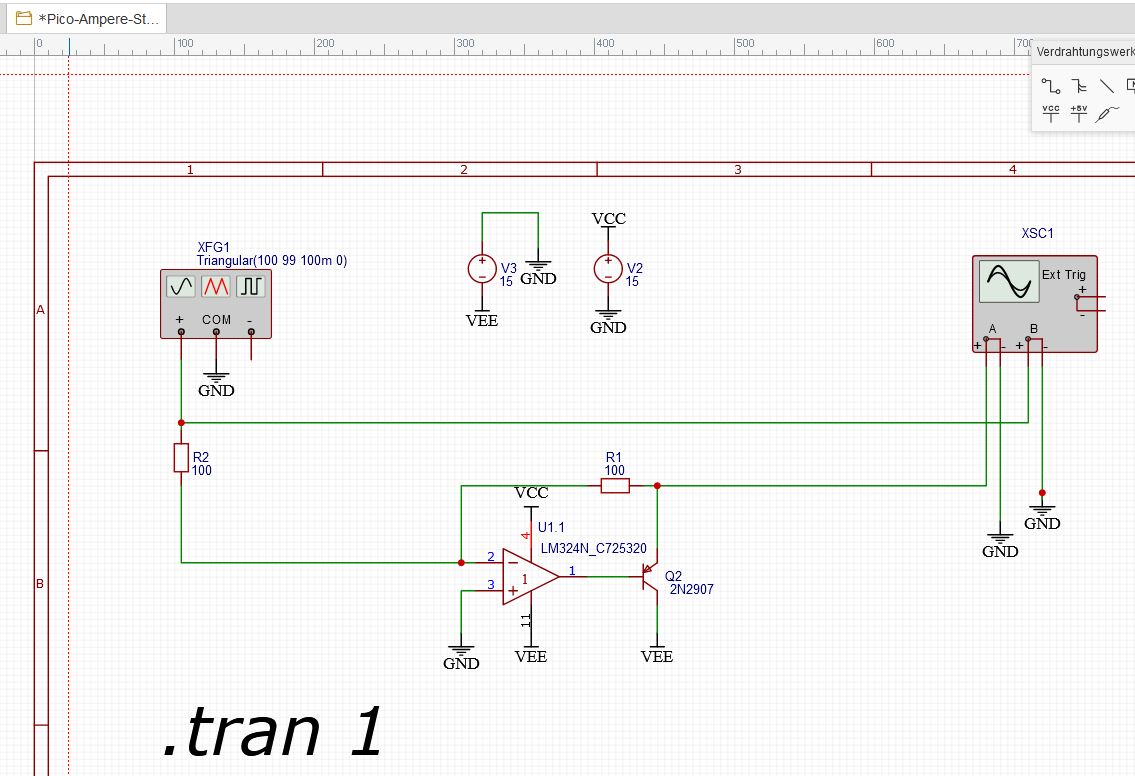
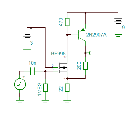
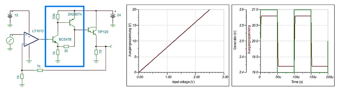
Ups. Mal davon abgesehen, dass der 2N2907 den Laststrom gar nicht aushält und dass der Basiswiderstand fehlt... *Hust*
bereit, selbst zu coden bzw. bevorzugst du GitHub als Lehrmeister, sprich referenzieren und läuft? 2) Im Gegensatz dazu, wie nah an die Hardware-Ebene musst du ran? Z.B. wenn es um Geschwindigkeit geht und um Genauigkeit Beispiel zu (2): Wenn du nen A/D-Wandler vom ESP32 relativ genau brauchst (besser
Werkzeug, hast du es gut, weil sich 98% aller Probleme als unlösbar entpuppen werden und du dich auf die 2% Rest konzentrieren kannst. Ich sage es mal so, wenn es mehr als Blinkenlight sein soll, wirst du mit der A-IDE so schnell vor die Wand klatschen, dass du nichtmal mehr "grunz!" machen kannst.
ich R3 mit 11k dimensionieren - damit wäre der Strom durch R3 auf etwa 2.5mA festgesetzt. Damit gehen etwa 2,45mA durch die LT1009-2.5 und die restlichen 0.05mA durch die Basis, wenn man ein B von 200 für den 2N3904 annimmt, bei einem zu erreichenden Kollektorstrom von 10mA
(mit den zwei 2N2907). Die Ursache der Schwingneigung wird vmtl. immer noch an der ungenügenden Abblockung der Versorgungsspannung liegen.
vielleicht mit 13. Gehalt, Urlaubsgeld, Weihnachtsgeld zu tun. Oder kommt das da noch dazu? Also, 18,5*2 wären 3600/Monat = 43k/a bei 37h.
ist Der Begriff "Wanderarbeiter" ist zutreffend (im 21. Jh. in einem OECD Land) bei über 65k € p.a. und 40 Std./Woche. Der Werk-/Dienst-/AÜG- Vertrag läuft ca. 6 Monate. Evt. Verlängerung. Kündigungsfrist 2 Wochen. Dann muss der DL zusehen wo er mich woanders unterkriegt. Meine Reisetasche liegt
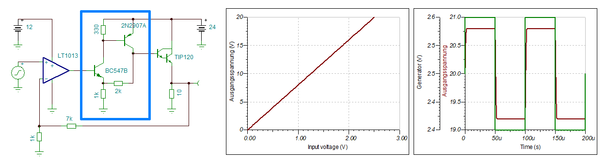
Du hast eine Last die 11.6A benötigt. Ausgang 20V / 2.4A (gemessen). Ausgang 2..5 regeln dann auf 2.3A.
dauerkurzschlussfest sein - Spannungsschwankungen von 0,5 - 1V sollten noch gehen - ich will es mit 12 x 2N3773 Transistoren regeln, welche bereits auf Kühlkörpern angebracht sind (soll auch aktiv gekühlt werden) - Den Gleichrichter wollte ich mit 2 x 30A Gleichrichtern parallel Gestalten - Glättung dachte
> Allerdings wird der 2N2222A ziemlich heiß Dann eventuell R4 etwas vergrößern, auch wenn die Leistung vorerst nachläßt. > Die Basisspannung am 2N2222 kommt mir mit 599mV recht hoch vor Durch Gleichrichteffekte geht
QRP-Sender vorgestellt, der auf 80, 40, 30 und 20m eine Ausgangsleistung von 1,5W liefert (PA-Transistor 2N3553, 2N3866, KT606A o.ä.). Es wird im Anhang eine Treiberstufe gezeigt, die auch als QRPP-Sender (150mW) benutzt werden kann und mit einem *2N2222* betrieben wird. Die Spannung am Punkt 1 dürfte
of the sec- Using Cascade Linearization ond amplifier (ve2, and then using a simple 1:1 widebandtransformertoinvertv andce2ductit tothebaseofthefirstamplifier. ShowninFig.3, this method results in a substantial reduction in theamplifierinputresistance: r e =
KMF 13S-LPM03 S D 0 2 A1 2 A-TYPE R 2 1 0 K 0.6A 7 D201 1 R 1 G C208 LGP3739I-13PL1 100uF/500V NZE 13S-LPM03 1 8 5 8 MBRF20200CT C203 1 K 0 V 100uF 2 8 2 2 2 C C224 0 0 0 0 D 470uF 2 6 D 1 C207 50V 0 4 2 . W 2 N 0.1uF D R
, 3.0V and 2.5V versions available as stan- u dard products. ■ Palmtop/Laptop Computer t ■ Personal Digital Assistant (PDA) R ■ Camcorder, Personal Stereo, Camera e u a Block Diagram t r I n S O - 3 a c a g e 1207801
. DESCRIPTION handbook,1halfpage 3 2 NPN switching transistor in a TO-18 metal package. PNP complement: 2N2907A. 2 3 MAM264 1 Fig.1 Simplified outline (TO-18) and symbol. QUICK REFERENCE DATA SYMBOL PARAMETER CONDITIONS MIN. MAX. UNIT VCBO
. DESCRIPTION handbook,1halfpage 3 2 NPN switching transistor in a TO-18 metal package. PNP complement: 2N2907A. 2 3 MAM264 1 Fig.1 Simplified outline (TO-18) and symbol. QUICK REFERENCE DATA SYMBOL PARAMETER CONDITIONS MIN. MAX. UNIT VCBO
. DESCRIPTION handbook,1halfpage 3 2 NPN switching transistor in a TO-18 metal package. PNP complement: 2N2907A. 2 3 MAM264 1 Fig.1 Simplified outline (TO-18) and symbol. QUICK REFERENCE DATA SYMBOL PARAMETER CONDITIONS MIN. MAX. UNIT VCBO
#5381887: > 1W Leistungsaufnahme zum Dekodieren http://d1jy6p8pks3hof.cloudfront.net/datasheets/T2L4A/Product%20Specification_T2-L4A-8650C__I_20130527.pdf 60 mW
Stefan H. schrieb im Beitrag #5381926: > http://d1jy6p8pks3hof.cloudfront.net/datasheets/T2L4A/Product%20Specification_T2-L4A-8650C__I_20130527.pdf > > 60 mW Nö. Drei Betriebsspannungen nötig und der typ. Strombedarf des KeyStone Chips ist im DAB Betrieb lt. Datenblatt: 1,2V : 48mA
grobe Anhaltspunkte): (Tabelle mit Klick auf Überschrift sortierbar) Bezeichnung Typ Pinbelegung I C /A V CE /V hFE ( ) V CEsat P tot /W f G /MHz Bemerkung 2N2222A NPN EBC 0,6 40 100 - 300 2N3904 NPN EBC 0,2 40 100 - 300 0,2 1,5 300 Komplementär 2N3906 2N5551 NPN EBC 0,6 160 150 - 200 S8050 (SS8050) NPN
50Ω, with rise and fall times inside 15 ns and clean settling characteristics. www.national.com 2 A N 2 7 2 00563003 PNP=2N2905 NPN=2N2219 unless noted TO-5 heat sinks for Q6-Q7 FIGURE 3. 3 www.national.com 7 - N A 00563004 FIGURE 4. Voltage-Current Booster In many applications it is desirable to
end of the charging interval, the V/I converter is minus sign in the MSD. The BCD code is 1010 for a negative connected from the integrating capacitor, and a band gap overrange (---) and 1011 for a positive overrange (EEE). NOTE 1 NOTE 2 +5V 0.1 0.27µF µF COMMON POWER ANODE LED 2N2907, 2N3906 DISPLAYS
2.5 -- Attib & Share Alike This is the 'universal' code designed for v1.2 - it will select EU or NA depending on a pulldown resistor on pin B1 ! */ #include <avr/io.h> // this contains all the IO port
2.5 -- Attib & Share Alike This is the 'universal' code designed for v1.2 - it will select EU or NA depending on a pulldown resistor on pin B1 ! */ #include <avr/io.h> // this contains all the IO port
A Vout=5.0V ( C 0.2 IL=5.0mAto40mA N 80 E I A 0 C L E O –0.2 E70 T R U –0.4 Vin10V L L =40mA T Vout5.0V P f=120Hz U L =5.0mAto100mA R V =10V ,t–0.6 R 60 V =14Vto24V o R in V –0.8 –1.0 50 –50 –25 0 25 50
kleiner, nur HF, ohne Sichtgerät, SWP-B1. https://www.ebay.de/sch/i.html?_nkw=Rohde+%26+Schwarz+%2A%C2%A0Polyskop+SWOB+3+-+Wobbelgenerator+%2F+SWEEP+Generator+%2A+0%2C1-1000
start-up during initial power R Q S 1M BF862 application. EDN G D 0.3 TO R 1.6IN D6 D 51 + 5 TO R 1N4148 1N4148 1 10 F 3 5 3 5VOUT 2 mA D5 MAXIMUM 2 1N4148 D1 TP0610L 4 7 6 1N5817 D2 D + S D + 1 D 3 1N751 G C1 G C2 1N41485.1V 6.8 F 100 F TO VIN 3 12 S D G R1 PRIMARY SECONDARY C4 3.83M TO Q 6 9 +1 F
end of the charging interval, the V/I converter is minus sign in the MSD. The BCD code is 1010 for a negative connected from the integrating capacitor, and a band gap overrange (---) and 1011 for a positive overrange (EEE). NOTE 1 NOTE 2 +5V 0.1 0.27µF µF COMMON POWER ANODE LED 2N2907, 2N3906 DISPLAYS
(°C) VinV outNPUT VOLTAGE DIFFERENTIAL (Vdc) Figure 7. Load Regulation Figure 8. Current Limit 3.0 A E DV 0 100 mV ( 70 A N L E 65 V )2.5 IL= 3.0 A R T d C 60 P ( IL= 2.0 A I U I P 55 − NT2.0 N T E E 50 P E I = 500 mA T , I L U 45 u D1.5 D Vo ,j 40 −i A V I = 20 mA L = 200 mA I 1.0 L 35−75 −50 −25 0
2,50 € IR2153 Halbbrücke mit Oszillator 100/210mA 600V n/a DIL8/SO8 Rei Con 1,20 € IR2155 Halbbrücke mit Oszillator 210/420mA 600V n/a DIL8/SO8 Rei Con 3,50 € IR2181 High + Low 1.4A/1.8A 600V 3,3V/5V DIL8
NOTE 2 +5V 0.27F 0.1 F COMMON POWER ANODE LED 2N2907, 2N3906 DISPLAYS OR EQUIV. MSD NSD LSD NORMAL 8 9 12 14 16 LOW SPEED MODE: V6 = GROUND OR OPEN a a a 5 f b f b f b HOLD: g g g V6= 1.2V 6 3 e c e c e c
4.0 ) ( 0.4 E ) N 0.2 ( 3.0 H N C 0 I = 0.5 A R T = 25⋅C G L R J T -0.2 C 2.0 O I = 1.5 A U V L T 150⋅C U -0.4 U T Vin 15 V ,t -55⋅C O -0.6 Vout= 10 V o 1.0 ,t I o-0.8 V -1.0 0 -50 -25 0 25 50 75 100 125 150 0 10 20 30
E ) N 0.2 ( 3.0 H N C 0 I = 0.5 A R T = 25⋅C G L R J T -0.2 C 2.0 O I = 1.5 A U V L T 150⋅C U -0.4 U T Vin 15 V ,t O -0.6 Vout= 10 V o 1.0 55⋅C ,t I o-0.8 V -1.0 0 -50 -25 0 25 50 75 100 125 150 0 10 20 30
low. TxD only goes low when the bus is pulled below 0.6 V.) Current flows in the led of the upper 6N137, causing the right hand bus to be pulled low. A low on the right hand bus turns on the 2N2907 and the led in the lower 6N137. In turn, that pulls the RxD input to the P82B96 low. While there is a
low. TxD only goes low when the bus is pulled below 0.6 V.) Current flows in the led of the upper 6N137, causing the right hand bus to be pulled low. A low on the right hand bus turns on the 2N2907 and the led in the lower 6N137. In turn, that pulls the RxD input to the P82B96 low. While there is a
InputWidebandNoisevs.Bandwidth Figure22.OutputShort-CircuitCurrentvs.Time (0.1HztoFrequencyIndicated) 32 1.50 T = 25°C TA= 25°C A 28 VS= ±15V VS= ±15V 1.25 ) ( E24 U I 1.00 L20 P ) A A K16 ( 0.75 A IB E -12 IB1– (nA) T 0.50 IB2– (nA) - I 3– (nA) A 8 B E IB1+ (nA) P 0.25 IB2+ (nA) 4 0 IB3+ (nA) 3 - 9 2 2 0 0 0 0 –16 –14 –10 –6 –
ALTERNATE FIELD IN-HOUSE IN-HOUSE REPLACEMENT ORDER NUMBER NUMBER NUMBER NUMBER NOTES TO-92 TRANSISTORS 2N3391(A) SPS-953(A, B) MPS-A18, 2N6539, OBSOLETE LEAD CONFIG. DIFF. ON MPS-8097, 2N6520 SK-3919 70403919 3391 2N4249 SPS-690, 699-1, 2N5086, 2N4249 70404249 REPLACE WITH SPS PN-2907A 761 IN DIF. AMPS
ALTERNATE FIELD IN-HOUSE IN-HOUSE REPLACEMENT ORDER NUMBER NUMBER NUMBER NUMBER NOTES TO-92 TRANSISTORS 2N3391(A) SPS-953(A, B) MPS-A18, 2N6539, OBSOLETE LEAD CONFIG. DIFF. ON MPS-8097, 2N6520 SK-3919 70403919 3391 2N4249 SPS-690, 699-1, 2N5086, 2N4249 70404249 REPLACE WITH SPS PN-2907A 761 IN DIF. AMPS
KW V = 5 V CC VCC1 = 5 V SU01022 Figure 4. Galvanic isolation of I 2C nodes via opto-couplers +5 V 6N137 +5 V x 2 *0.1 ▯F 2K2 560 560 USUAL I C PULL-UP USUAL I C PULL-UP 2 IC SDA I C SDA (SDA) 6 7 8 2 Rx (SDA) *0.1 ▯F 1/2 P82B96 5 3 2N2907 *NOTE: 6N137 data recommends 0.1 ▯F mounted between pins 5 and 8 SU01015 2 Figure 5. Opto-isolation of I C nodes via 6N137 for 100 kHz operation 2001 Feb 14 3 Philips Semiconductors Application note Using the P82B96 for bus interface AN460 LINK VIA A DIFFERENTIAL BUS TECHNICAL
2.4 V IN.6V FB=1.0V 2.2 ) 12.0 ) 2.0 SHDN=1.0V ( A e ( 1.8 t n o e 1.6 V 11.5 u u C 1.4 t l 1.2 u p O 11.0 u 1.0 S 0.8 10.5 0.6 1 10 100 2 3 4 5 6 7 8 9 10 11 Output Current (mA) Supply Voltage (V) Fig
need to be replaced, please also check the driver transistors and control IC. The Q46and Q48 are (2SC2655 2A 50V NPN TAP TO-92) The Q47and Q49 are (2SA1020L-Y-T9N-B 2A 50V PNP TAP TO-92NL) The Q41and Q43 are (2SC2655 2A 50V NPN TAP TO-92) The Q15and Q16 are (2SA1020L-Y-T9N-B 2A 50V PNP TAP TO-92NL)

 Bild
Bild
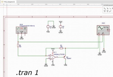
 Bild
Bild
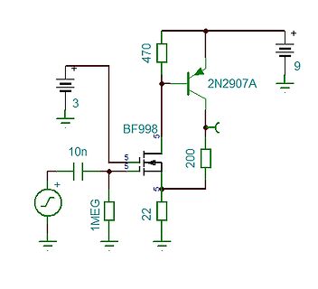
 Bild
Bild
 Bild
Bild
 Bild
Bild