, merkte ich, ich hab den Durchblick völlig verloren. In der Firma war aber eine Lizenz des Keil C51 verfügbar und so habe ich damit gearbeitet. Es ist mir sprichwörtlich die Kinnlade runtergefallen, so kompakt und effizient hat der Herr Keil programmiert. Ich konnte das Projekt nun problemlos beenden
= PIN1_bm | PIN2_bm; while(1) { PORTA.OUTTGL = PIN1_bm | PIN2_bm; _delay_ms(500); } } [/c] Das Hauptprogramm kompiliere ich mit -Wl,--section-start=.text=0x0080 Die Headerdatei fuses.h ist bei Bootloader und Hauptprogramm gleich und setzt FUSES.BOOTEND auf 1: [
das nichts ausmacht: gerne ! F. schrieb im Beitrag #7861989: > Denk nur mal an den grausigen 80C51 Die waren nicht grausig, ich habe die "geliebt". Zudem bin ich bis heute dem Intel-Stil der Mnemonic verhaftet, egal ob das 8080, MCS-48 (jaja, den habe ich auch noch gemacht), MCS-51 oder später
OP 11 15 19.4 mA Operating Current Low DD low B<B RP 3.9 5 6.9 mA Data Valid Delay TDLY DB>B hys 25 ms o Thermal Resistance RTH Operating SO Package 575 C/W Thermal Resistance RTH Operating UA Package 206 oC/W # MLX90223 Magnetic Specifications o DC Operating Parameters: T = -A0 to 85 C, V DD = 3.75 to
approx. 0.5MHz A: 0.5s – 50ns/div. parameter selection Sum or Difference: from CH I and CH II B: 20ms – 50ns/div. Save & Recall: 9 user defined parameter settings Invert: CH I and CH II Operatingmodes: A or B, alternate A/B XY-Mode: via channel I (Y) and channel II(X) Variable: 2.5:1 up to 1.25s/div.
Drain D Power Dissipation (Note 1) t v 5 s P D 0.33 W SC−70/SOT−323 T4 WG Pulsed Drain Current tp= 10 ms IDM 3.0 A G CASE 419 Operating Junction and Storage Temperature T J −55 to °C STYLE 8 T STG +150 1 2 Gate Source Source Current (Body Diode) (Note 1) S 0.3 A Lead Temperature for Soldering Purposes TL
– 0.3 to + 7 V o Pulsed Output Current for L6201PS/L6202/L6203 (Note 1) 5 A – Non Repetitive (< 1 ms) for L6201 5 A for L6201PS/L6202/L6203 10 A DC Output Current for L6201 (Note 1) 1 A Vsense Sensing Voltage – 1 to + 4 V V Boostrap Peak Voltage 60 V b Ptot TotalPower Dissipation: T pins 90⋅C for L6201
1 1 1 1 1 E 3 3 4TSET 62FA R R R R R R C C C C C C C C SSV 3 3 1FA 45 SSV 0KCRL 14 SSV CN K 1KCRL 51A 82 04 C 51B 25 QSSV D 6 7 2KCRL 51C 6 QSSV CN 63 . 1 1 64 QSSV +3 R R 11A OKCSYS 0KC W 41D 21 QSSV D 1KC W 31A 1 0 0 0 0 0 0 0 81A TROP 2KC W 31B D 42A MWP MQDL 51 0KCS 41A 34 QDDV MQDU 93 9A CNYS 1KCS
390K metal R 5 * 2,2K R 6 0,22 1 + 2x 0,56 parallel R 7 * 2,2K R 8 * 7,5K R 9 3,3 R 10 18K R 11 * 51K metal R 12 * 3825K 2x 1,91M metal R 13 * 3825K 2x 1,91M metal R 14 * 51K metal R 15 0,50 2x 1 parallel R 16 * 390K R 17 18K R 18 3,3 R 19 5,1K metal R 20 5,1K metal R 21 10K R 22 680 R 23 * 33K R 24 * 51 K metal R 25 * 10K R 26 * 68K R 27 * 51K metal R 28 4,7K R 29 1 R 30 SIOV-S14K250G5 Q69x4603 EPCOS R 31 insert wire bridge R 32 * 1,1K R 33 470 R 34 * 56K R 35 * 1,1K R 35A * 680 R 36A 56 4W R 37 3,9K
0204 L W l u P 10 u u i n 1 o C 0.1 10 µs 100 µs 1 ms 10 ms 100 ms 1 s 10 s Pulse Duration i Maximum pulse load, continuous pulses; for permissible resistance change equivalent to 8000 h operation. Continuous Pulse x a m MBE/SMA 0414 e MBB/SMA 0207 g MBA/SMA 0204 l V 1 kV e l P 100 V 10 µs 100 µs 1 ms 10 ms 100 ms 1 s 10 s Pulse Duration i Maximum pulse voltage, single and continuous pulses; for permissible resistance change equivalent to 8000 h operation. Pulse Voltage Revision: 02-Nov-15 9 Document
1 1 1 4 4 4 4 4 4 4 4 E 3TSET 62FA D R R R R R R C C C C C C C C 3 3 4TSET 1FA 45 SSV 14 SSV 0KCRL 51A 82 SSV CN 04 K 1KCRL 51B 25 QSSV D 2KCRL 51C QSSV CN . 2 2 6 QSSV 63 3 1 1 OKCSYS 0KC W 64 QSSV + R R 11A 1KC W 41D 0 . . . . . . . 21 D TROP 2KC W 31A 1 0 0 0 0 0 0 0 81A MWP 31B MQDL D 42A 0KCS 51
250 - 300 ns CC V CC= 4.5 V - 18 50 - 60 ns V CC= 5 V; CL= 15 pF - 15 - - - ns V CC= 6.0 V - 14 43 - 51 ns nRD to nQ, nQ; see Fig. 8 [2] V CC= 2.0 V - 52 250 - 300 ns V CC= 4.5 V - 19 50 - 60 ns V CC= 5 V; CL= 15 pF - 16 - - - ns V = 6.0 V - 15 43 - 51 ns CC t transition time nQ, nQ; see Fig. 7 [3] V CC
Supply Sequencing and Ramp Rates (1) PARAMETER MIN TYP MAX UNIT VCC_FT Fall rate See Figure 23 1 100 ms VCC_RT Rise rate See Figure 23 0.01 100 ms V Time to re-ramp (when V drops to GND) See Figure 23 0.001 ms CC_TRR_GND CC VCC_TRR_POR50 Time to re-ramp (whenCC drops to POR_MIN– 50 mV) See Figure 24 0.001 ms V Level thatCCP can glitch down to, but not cause a functiSee Figure 25 1.2 V CC_GH disruption whenCCX_GW = 1 μs V Glitch width that will not cause a functional disruptionSee Figure 25 μs CC_GW VCCX_GH
C-bus protocol as to how long this delay can be, whereas for a SMBus system, it would be limited to 35 ms. SMBus protocol just assumes that if something takes too long, then it means that there is a problem on the bus and that all devices must reset in order to clear this mode. Slave devices are not then
Maximum Clock Temperature Available Packages Frequency Ranges 24AA256 1.7V-5.5V 400 kHz (1) I, E CS, MF, MS, P, SN, SM, MNY, ST 24LC256 2.5V-5.5V 400 kHz I, E MF, MS, P, SN, SM, MNY, ST (2) 24FC256 1.7V-5.5V 1 MHz I, E MF, MS, P, OT, SN, SM, MNY, ST Note 1: 100 kHz for V CC < 2.5V. 2: 400 kHz for V CC < 2.5V
Offset Current V CM = 0V, o = 0 mA 0.01 0.2 μA (max) o Output Current Limit |V | = |V | = 20V,ON = 10 ms, VO= 0V 11.5 7 A (min) (8) (9) + + Vod Output Dropout Voltage |V –V O, V = 28V, Io= +100 mA 1.6 2.0 V (max) |VO–V |, V = −28V, I o −100 mA 2.5 3.0 V (max) (8) + − PSRR Power Supply Rejection Ratio V
ISO T/R Test levels 7637/1 test pulse I II III IV Delays and impedance 1 -25 V -50 V -75 V -100 V 2 ms, 10 Ω 2 +25 V +50 V +75 V +100 V 0.2 ms, 10 Ω 3a -25 V -50 V -100 V -150 V 0.1 µs, 50 Ω 3b +25 V +50 V +75 V +100 V 0.1 µs, 50 Ω 4 -4 V -5 V -6 V -7 V 100 ms, 0.01 Ω 5 +26.5 V +46.5 V +66.5 V +86.5 V
T/R Test levels 7637/1 test pulse I II III IV Delays and impedance 1 - 25V - 50 V - 75 V - 100 V 2 ms, 10 Ω 2 + 25 V + 50 V + 75V + 100V 0.2 ms, 10 Ω 3a - 25 V - 50 V - 100 V - 150 V 0.1 µs, 50 Ω 3b + 25 V + 50 V + 75 V + 100 V 0.1 µs, 50 Ω 4 - 4 V - 5 V - 6 V - 7 V 100 ms, 0.01 Ω 5 + 26.5 V + 46.5 V
System regulation ∙ R 1.3∙V R 1 min System regulation NOTE 1 An overvoltage equal to∙1.R V for 30 ms is permitted 1000 times during the life of the capacitor. The amplitudes of the overvoltages that may be tolerated without significant reduction in the life time of the capacitor depend on their duration
filter capacitor. POWER 10 AGND Input 0V Analog ground. 1,5,11,15, POWER GND 0V Ground input. 25,35,47,51 Input Table 3.2 Power and Ground for 64-pin QFN and LQFP package Pin No. Name Type Description 2 OSCI INPUT Oscillator input. 3 OSCO OUTPUT Oscillator output. 6 REF INPUT Current reference – connect
Netzteil Meanwell SP-200-3,3 3,3V 40A Bilder findet man unter folgendem Link: https://1drv.ms/f/c/0da3416c8d6e51b4/Et06BBEN2PJHlK8nkL4e0soB_HtOFyDFEVed24XhG3EjtA?e=486ypV
mm dimensions) UNIT A A 1 A2 b b c D(1) E(1) e e L M M w Z(1) max. min. max. 1 1 E H max. mm 4.7 0.51 3.7 1.40 0.53 0.32 21.8 6.48 2.54 7.62 3.9 8.25 9.5 0.254 2.2 1.14 0.38 0.23 21.4 6.20 3.4 7.80 8.3 inches 0.19 0.020 0.15 0.055 0.021 0.013 0.86 0.26 0.10 0.30 0.15 0.32 0.37 0.01 0.087 0.045 0.015
eines simplen Ladewiderstandes und einem DW01 schaltet der bei erreichen von 4,25V (max 4,30V) nach 80ms (max 200ms) ab. Da bin ich mir nicht sicher was die Lebensdauer stärker verkürzt.
simplen Ladewiderstandes und einem DW01 schaltet > der bei erreichen von 4,25V (max 4,30V) nach 80ms (max 200ms) ab. > > Da bin ich mir nicht sicher was die Lebensdauer stärker verkürzt. Musst Du nicht. Ich bin mir zumindest sicher, dass Du die Li-Ladetechnik nicht verstanden hast. Ein DW01
-3 3300Hz -34 Carrier Detect Sensitivity 5V ¾ -48 ¾ dBm tDOSC Oscillator Start Up Time 5V ¾ ¾ 2 ¾ ms tSUPD Power Up to FSK Signal Set Up Ti5V ¾ 15 ¾ ¾ ms tDAQ Carrier Detect Acquisition Time 5V ¾ ¾ 14 ¾ ms tDCH End of Data to Carrier Detect Hi5V ¾ 8 ¾ ¾ ms Rev. 1.70 4 February 26, 2020 HT9032C/HT9032D
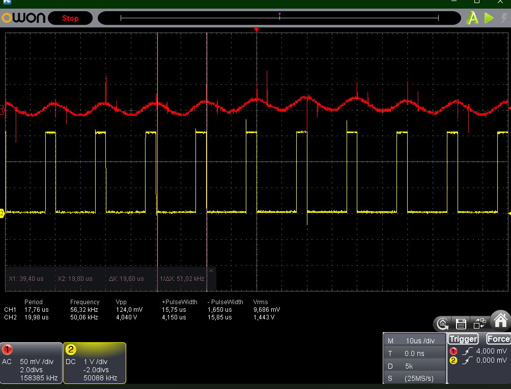
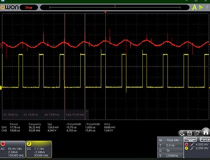
won Stop A X1: 39,40 us X2: 19,80 us ΔX: 19,60 us 1/ΔX: 51,02 kHz Period CH1 17,76 us CH2 19,98 us Frequency 56,32 kHz 50,06 kHz Vpp 124,0 mV 4,040 V +PulseWidth 15,75 us 4,150 us -PulseWidth 1,650 us 15,85 us Vrms 9,686 mV 1,443 V AC 50 mV/div DC 1 V/div 2.0divs -2.0divs 158385 kHz 50088 kHz M T 0.0 ns D 5k S (25MS/S) Trigger Force 1 4,000 mV 2 0,000 mV
Auswertung s16 DigPotWert_alt ; u32 acttick ; s16 diff ; // Digitalpoti Differenz der letzten 200 ms s16 ddiff ; // Digitalpoti dynamische Differenz der letzten 200 ms #define POTIFAKTOR 4 // Das POTI ist ansonsten zu langsam u32 startsectick ; u32 max_difftick ; u32 max_difftickLCD ; u16 anzeigesec
filter capacitor. POWER 10 AGND Input 0V Analog ground. 1,5,11,15, POWER GND 0V Ground input. 25,35,47,51 Input Table 3.2 Power and Ground for 64-pin QFN and LQFP package Pin No. Name Type Description 2 OSCI INPUT Oscillator input. 3 OSCO OUTPUT Oscillator output. 6 REF INPUT Current reference – connect
for MAX692A/MAX802M control functions in microprocessor (μP) systems. They ●● Reset Time Delay: 200ms significantly improve system reliability and accuracy ●● Watchdog Timer: 1.6s Timeout compared to separate ICs or discrete components. ●● Battery-Backup Power Switching These parts provide four functions
Hallo zusammen, Nachdem ich die Zündsignale vom S51 auf den Arduino bekommen habe hatte ich heute mir mal die scheinbar stehende Welle angeschaut. Leider ist das Ergebnis mit meinen 6 weißen LED‘s bei 33 Hz / 4 ms blitzen nicht grad berauschen und gut
4ms ist viel zu lange, man will eher 0,1ms. Damit das noch hell genug ist, brauchst du viel mehr Leistung. Wie hast du denn die LEDs angesteuert?
Das klappt aber dann nur im Mittel bzw. bei langen Zeiten. Bei einer > kurzen Zeit - sagen wir 10ms - ist der Fehler dann schon eheblich > gegenüber der angeblichen Genauigkeit von 5ppm. Bei 10 ms ist der Fehler (Jitter) 0,3%, was eigentlich nicht schlecht und besser als die ms Auflösung des 1
Axel S. schrieb im Beitrag #7830896: > Wenn man wie der TO 1,000000ms Auflösung bei gleichzeitig hoher > Genauigkeit will Dann ist immer noch die Frage, ob man diese ultraexakte 1,000000ms tatsächlich überhaupt *braucht*. Denn die Abtastung mit exakt 1,000000ms ergibt
Note 13) 400 pF Line SCL Spike Suppression tSP 60 ns Oscillator Stop Flag (OSF) Delay t (Note 14) 100 ms OSF Timeout Interval tTIMEOUT (Note 15) 25 35 ms Maxim Integrated 3 www.maximintegrated.com DS1308 Low-Current I C RTC with 56-Byte NV RAM Power-Up/Down Characteristics (TA= -40NC to +85NC, unless otherwise noted.) (Notes 2, 16) PARAMETER SYMBOL MIN TYP MAX UNITS Recovery at Power-Up tREC 1 2 ms V Slew Rate (V to 0V) t 1/50 V/Fs CC PF VCCF VCC Slew Rate (0V to PF) tVCCR 1/1 V/Fs Capacitance (T = +25NC, unless otherwise noted.) (Note 16) A PARAMETER SYMBOL MIN TYP MAX UNITS Input Capacitance

 Bild
Bild
 Bild
Bild
 Bild
Bild