aber um folgenden Sensor in der 1000mm Ausführung: https://www.amazon.de/gp/product/B08J3H1N11/ref=ppx_yo_dt_b_asin_title_o02_s00?ie=UTF8&th=1 Im letzten Jahr habe ich den IBC noch per kapazitiven Sensor aus dem Homematicbaukasten überwacht, doch schwankte der Messwert sehr stark, je nachdem,
Wenn das wie schon mal gesagt 12V und 2.2kΩ sind, dann schwankt der Strom zwischen 5.45mA und 5.02mA (wenn der Sensor seinen Widerstand von 0..190Ω verändert). Entsprechend gibt es eine kleine Nichtlinearität. Wenn die wirklich stört, dann den Vorwiderstand durch eine Stromquelle ersetzen. Schaltungen
Dokument, Kapitel Eichschein Seite 20: https://amarell-thermometer.de/wp-content/uploads/2021/12/02-innenteil_2021-labortherm.pdf
https://www.amazon.de/Xiaomi-NUN4126GL-Temperatur-Feuchtigkeitsmonitor-wei%C3%9F/dp/B08C7KVDJW/ref=asc_df_B08C7KVDJW (nur im Original Xiaomi Shop sonst gefälscht) mit SHT30 greifen für +/-0.5K.
MB_ series has been merged with the related SMA series to form one series “MB_/SMA__”. (2) Please refer to APPLICATION INFORMATION below. Revision: 02-Nov-15 1 Document Number: 28766 For technical questions, contact: filmresistorsleaded@vishay.com THIS DOCUMENT IS SUBJECT TO CHANGE WITHOUT NOTICE. THE
assembler supports labels: You can assign a name to a certain code location, and use this name to refer to the code location instead of specifying the address as a number. A label is defined by writing its name followed by a colon: Example name: “Blink2” This is purely a feature of the assembler – the
label refers to code (and not data) via the already mentioned “.type” directive: That way, when you refer to the label to load its address into a register, the lowest bit will be set. Actually, using “.type” for all code labels is a good idea, even though it does not matter if you only refer to a label
listed in the figure, refer to the respective data sheet or contact your nearest Broadcom representative for details. 2. Bin options refer to shippable bins for a part number. Color and Intensity Bins are typically restricted to 1 bin per tube (exceptions may apply). Refer to respective data sheet for specific bin limit information. Broadcom AV02-4479EN 6 HLCP-A100/-B100/-C100/D100/-E100/-G100/-H100, HLMP-2300/-2350/-2400/ -2450/-2500/-2550, HLMP-2600/-2620/-2655/-2670
b 0.22 – 0.40 Terminal Thickness c 0.08 – 0.23 Terminal Length L 0.40 0.60 0.80 Footprint L1 0.95 REF Lead Bend Radius R 0.07 – – Lead Bend Radius R1 0.07 – – Foot Angle ș 0° – 8° Mold Draft Angle ș1 5° – 15° Notes: 1. Pin 1 visual index feature may vary, but must be located within the hatched area.
2C477&sr=8-1&th=1&linkCode=sl1&tag=shakeela65-21&linkId=6caee1a7cf14f17032b61a2820bbb3f2&language=de_DE&ref_=nav_signin Ich denke 250 € + Versand nach Wahl ist fair. Paypal oder Banküberweisung, wie gewünscht. Gruss Piefke
volle Gewährleistung für das Teil leisten möchte.😁 Zum TE: Lt. seinem PDF von Amazon hat er am 26.02.2025 gekauft, lt. keepa.com also für 249,-, lt. "Titel" erst am 28.02.2025, also im *Hochpreiszeitraum* für 899,-€. Also ist das Absicht oder total verblödet..
Exposure to Absolute Maximum Rating conditions forns of extended periods may affect device reliability. Refer also to the STMicroelectronics SURE Program and other relevant quality document. Table 3. Absolute maximum ratings Symbol Parameter Value s Unit VCC DC supply voltage 41 c t( V - CC Reverse DC supply
Exposure to absolute maximum rating conditions for extended periods may affect device reliability. Refer also to the STMicroelectronics SURE Program and other relevant quality document. Table 3. Absolute maximum ratings Symbol Parameter Value Unit V CC DC supply voltage 41 V -VCC Reverse DC supply voltage
Exposure to absolute maximum rating conditions for extended periods may affect device reliability. Refer also to the STMicroelectronics sure program and other relevant quality document. Table 3. Absolute maximum ratings Symbol Parameter Value Unit V DC supply voltage 41 V CC - VCC Reverse DC supply voltage
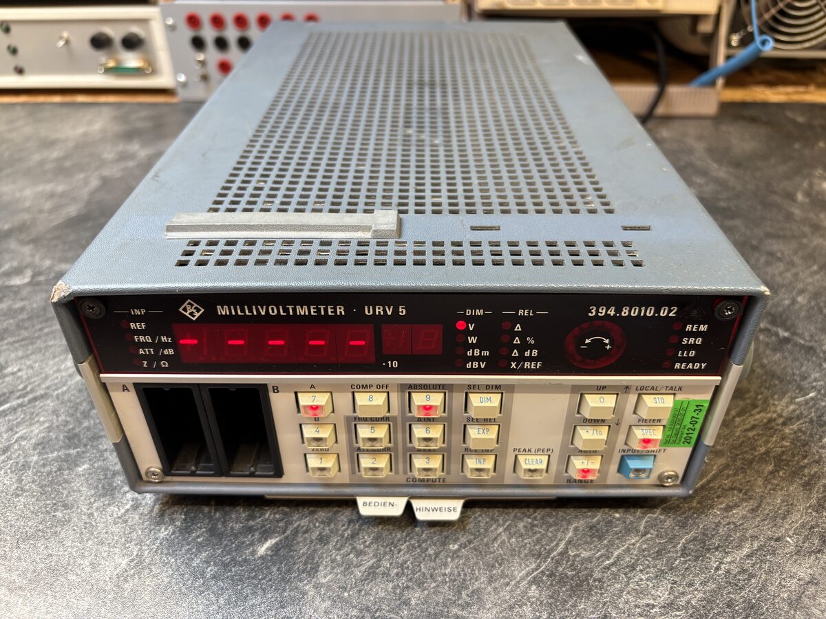
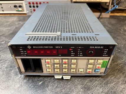
MILLIVOLTMETER URV 5 DIM - REL 394.8010.02
REF FRQ /Hz ATT /dB Z /Ω
V dBm dBV Δ Δ% Δ dB
REM SRQ LLO READY
COMP OFF ABSOLUTE SEC DIM UP LOCAL / TALK
8 4 2 1 0 10 FILTER
FREQ/CURR 5 3 1 EXP DOWN SELECT
SIGNAL 4 2 0 RANGE
INT
PEAK (PEAR)
Z /Ω
COMPUTE
body temperature (ambient temperature + self-heat- ing) must be observed for maximum voltage rating. Refer to voltage derating rules in page 20. 3) Typical ESL value measured at resonance frequency (see specific graphs of Z versus frequency). Please read Cautions and warnings and Important notes at the
) which may have been configured previous to any switching of channel A to Synchronous FIFO mode. Refer to AN1121C-01 MPSSE Cmnd for the set_data_bits command and further information on the MPSSE used in MCU Host BUS Emulation mode. The MPSSE can be configured directly using the D2XX commands. Refer
4.6. Crystal Oscillator Parameter Symbol Test Condition Min Typ Max Unit Crystal Frequency fXTAL 0.02 — 30 MHz 4.1.7 External Clock Input Table 4.7. External Clock Input Parameter Symbol Test Condition Min Typ Max Unit External Input CMOS Clock fCMOS 0 — 48 MHz Frequency (at EXTCLK pin) silabs.com |
The value read from this bit is indeterminate. Do not set this bit. 4 PSL Serial port Priority bit Refer to PSH for priority level. Timer 1 overflow interrupt Priority bit 3 PT1L Refer to PT1H for priority level. External interrupt 1 Priority bit 2 PX1L Refer to PX1H for priority level. 1 PT0L Timer 0
150 mA Output Power P 600 600 mW S, OUTPUT Insulation Resistance at S, VIO= 500V RS >109 >10 9 Ω a. Refer to AV02-2041EN, Avago Technologies Regulatory Guide for Isolation, (IEC/EN/DIN EN 60747-5-5) for a detailed description of Method a and Method b partial discharge test profiles. Note: Isolation characteristics
PCF8574 NOTES 1997 Apr 02 22 Philips Semiconductors Product specification 2 Remote 8-bit I/O expander for I C-bus PCF8574 NOTES 1997 Apr 02 23 Philips Semiconductors — a worldwide company Argentina: see South America Netherlands
verwenden: 2,80€ für 3m 0,6mm mit 4,38R/m https://www.ebay.de/itm/253349283035 91cm davon haben 4,02R, macht 2,98A bei 12V entsprechend so 39W/m Für 1,1m Schneidlänge reicht das Netzteil nicht.
kupplung+und+20m+schlauch+set+kg+-+zerkleinerer+f%C3%A4kalienpumpe+schmutzwasserpumpe+pumpe+%2Cdiy%2C100&ref=nb_sb_noss Die hält so gut wie nichts auf. Davor hatte ich auch die ein oder andere für groben Schmutz versucht aber keine arbeitete wie gewüscht.
noch dümmer wirst. Wenn du vorher mal etwas gegoogelt hättest : https://www.noord360.eu/2021/02/10/guelletourismus-warum-deutschland-hunderttausende-tonnen-guelle-aus-den-niederlanden-importiert/ Wenn man googelt, findet man da auch noch mehr Beiträge.
) which may have been configured previous to any switching of channel A to Synchronous FIFO mode. Refer to AN1121C-01 MPSSE Cmnd for the set_data_bits command and further information on the MPSSE used in MCU Host BUS Emulation mode. The MPSSE can be configured directly using the D2XX commands. Refer
Stretched SOIC P2 P0 T D0 E 0.30 ±0.03 +0.10 2.00 ±0.10 4.00 ±0.10 1.75 ±0.10 1.50 0.00 Y D1 ) +0.20 REF 2.0 F 1.50 0.00 ) W ( o B 5 3 X X F TYP R0.30 R REF6.0 K1 Y Ao (V) Ko P1 SECTION Y-Y 45 ° $R ▯▯▯▯▯ ▯▯▯▯▯▯▯▯ %R ▯▯▯▯ ▯▯▯▯▯▯▯▯ SECTION X-X .R ▯▯▯▯ ▯▯▯▯▯▯▯▯ ▯,▯ 0HDVXUHG▯IURP▯FHQWUHOLQH▯RI▯VSURFNHW▯KROH
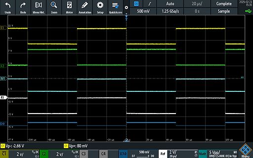
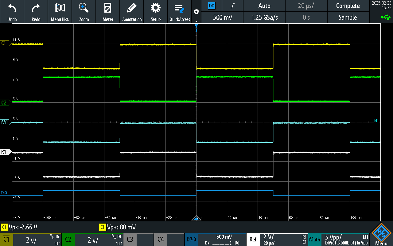
Zoom Meter Annotation Setup QuickAccess D0 500 mV Auto 1.25 GSa/s 20 us/ 0 s Complete Sample 2025-02-23 15:35 C1 11 V 9 V 7 V 5 V C2 3 V 1 V M1 -1 V R1 -3 V -5 V -7 V -100 us -80 us -60 us -40 us -20 us 20 us 40 us 60 us 80 us 100 us D7 500 mV 2 V/ 20 us/ Ref C1 Vp-: -2.66 C1 Vp+: 80 mV C3 C4 D7-0 R1
Output 1 7 n.c. Not connected 8 V Power Supply Voltage S 9 OUT2 Power Output 2 13 RANGE Range Input 14 REF Reference Input Data Sheet 2 V1.4, 2018-07-02 TLE 4206-2G Vs TLE 4206-2G 8 RANGE 13 Range- AMP Half- 6 Bridge OUT1 REF 14 Servo- Protection and FB 1 AMP Logic 9 Half- OUT2 Bridge HYST 2 Hyst- AMP 3,4,5
= C2 = SANYO OS-CON D1 = MOTOROLA MBRS130LT3 LOAD CURRENT (mA) L1 = COILTRONICS CTX10-3 LT1302 • TA02 COILCRAFT DO3316-103 Figure 1. 2-Cell to 5V/600mA DC/DC Converter 1 LT1302/L T1302-5 W W W U U W U AB S O LU ET A XI U RA T I G S PACKAGE /O RDER I FOR ATIO TOP VIEW V INltage .......................
= C2 = SANYO OS-CON D1 = MOTOROLA MBRS130LT3 LOAD CURRENT (mA) L1 = COILTRONICS CTX10-3 LT1302 • TA02 COILCRAFT DO3316-103 Figure 1. 2-Cell to 5V/600mA DC/DC Converter 1 LT1302/L T1302-5 W W W U U W U AB S O LU ET A XI U RA T I G S PACKAGE /O RDER I FOR ATIO TOP VIEW V INltage .......................
August 2016 4 of 31 NXP Semiconductors PCA9532 16-bit I C-bus LED dimmer 6. Functional description Refer to Figure 1 “Block diagram of PCA9532”. 6.1 Device address Following a START condition, the bus master must output the address of the slave it is accessing. The address of the PCA9532 is shown in Figure
nicht hinreichend linear auf das Einstellpoti. Selbst mit 16 Gang Trimmer schafft man es kaum 20 +-0,02mA einzustellen weil der LM317 erst eine Weile nur sehr träge auf das Poti reagiert und dann plötzlich einen deutlichen Sprung macht. - Und der Wert verstellt sich auch zu stark von selbst obwohl die
weniger als 0.05% Schwankungen haben darf ? 0.1% initial genaue Referenzen sind selten, LM369, REF5050, LT1021C, LTC6655.
Figure 13. SMB package outline E1 D E A1 C A2 L b Table 3. SMB package mechanical data Dimensions (1) Ref. Millimeters Inches Min. Max. Min. Max. A1 1.90 2.45 0.0748 0.0965 A2 0.05 0.20 0.0020 0.0079 b 1.95 2.20 0.0768 0.0867 c 0.15 0.40 0.0059 0.0157 D 3.30 3.95 0.1299 0.1556 E 5.10 5.60 0.2008 0.2205
2 mA. I + I ) I + 10 ) 2 + 12 mA (12–7) REF D The value of RB1 is calculated in Equation 12–8, and the value of B2 is calculated in Equation 12–9. V * V R + )5 ref+ 5 * 2.495 + 208 W (12–8) B1 I 12 V R + ref+ 2.495 + 1247 W (12–9) B2 D 2 Both
The value read from this bit is indeterminate. Do not set this bit. 4 PSL Serial port Priority bit Refer to PSH for priority level. Timer 1 overflow interrupt Priority bit 3 PT1L Refer to PT1H for priority level. External interrupt 1 Priority bit 2 PX1L Refer to PX1H for priority level. 1 PT0L Timer 0
8.0 V (V ) SUV Minimum Supply to Enable Power 3.0 4.0 3.0 4.0 V OK Output REFERENCE Output Voltage (REF) T J 25°C 2.485 2.5 2.515 2.470 2.5 2.530 V Over Temperature 2.465 2.535 2.465 2.535 V Load Regulation IL = 0 to 10mA 1 10 1 15 mV Line Regulation +V IN= 8 to 40V 1 4 1 8 mV Short Circuit Current TJ
21) D D C NP91 2 1 0 2 R9 03 8 8 8 Q921 R9 02 T902 2 C 899 R R R 9 F C89 8 R92 3 C C92 3 C950 2 2 CN P903 3 R RD 914 D9 11 2 8 1 2 C J D915 D C D910 D9 12 G 901 G • Semiconductor Location Ref. No. Location D820 E-4 D821 E-5 D822 E-5 D823 E-4 D898
COM0A1)|(0<<COM0A0)|(1<<COM0B1)|(0<<COM0B0)|(1<<WGM01)|(1<<WGM00) ;TCCR0A out TCCR0A, AL ldi AL, (0<<WGM02)|(0<<CS02)|(0<<CS01)|(1<<CS00) ;TCCR0B /1 out TCCR0B, AL clr AL ;kein INT sts TIMSK0, AL ; Counter 2 Mode 3 ldi AL, (1<<COM2A1)|(0<<COM2A0)|(1<<COM2B1)|(0<<COM2B0)|(1<<WGM21)|(1<<WGM20) ;TCCR2A sts TCCR2A
4.6. Crystal Oscillator Parameter Symbol Test Condition Min Typ Max Unit Crystal Frequency fXTAL 0.02 — 30 MHz 4.1.7 External Clock Input Table 4.7. External Clock Input Parameter Symbol Test Condition Min Typ Max Unit External Input CMOS Clock fCMOS 0 — 48 MHz Frequency (at EXTCLK pin) silabs.com |
simulierten Flash zu übertragen, bekomme ich die Ausgabe [code] SSFE SSFE RSB 00 RSB 01 RSB 02 SSFE SSFE RSB 00 RSB 01 RSB 02 CE SSFE RPM 0004 00 RPM 0005 00 WPM 0 [/code] und nach der letzten '0' hängt das Programm. S. L. schrieb im Beitrag #7821738: > Nur Frage am Rande: was
absehbarer Zeit dazu komme. Da empfehle ich:[pre] ARM and Thumb-2 Instruction Set ARM_GNU_assembler_ref ARM ThumbRefCard ARM v6-M Architecture Reference Manual Cortex-M0+ Technical Reference Manual [/pre] Da hast du im Grunde genommen alles, was es braucht um den RP2040 zu programmieren. Für
Erfahrungen? Falls das eine Rolle spielt, es handelt sich um diesen: https://www.amazon.de/dp/B01MUFRHQ2?ref=ppx_yo2ov_dt_b_fed_asin_title&th=1 Danke für Eure Hilfe.
der Nachwuchs keine RTC einbauen wollte? Einigen wir uns auf 2 Stunden. Wenn man dann ungefähr um 02:00 die Tage runter zählt, stimmt der Zählerstand jedenfalls vor dem schlafen gehen und nach dem aufwachen.
SPICE modeling guideline and does not *constitute a commercial product datasheet. Designers should refer to the *appropriate datasheet of the same number for guaranteed specification *limits. .SUBCKT Si4497DY D G S M1 3 GX S S PMOS W= 20692500u L= 0.25u M2 S GX S D NMOS W= 20692500u L= 2.177e-07 R1 D 3 1.789e-05 3.229e-02 3.241e-05 CGS GX S 5.513e-09 CGD GX D 5.000e-10 RG G GY 2.3 RTCV 100 S 1e6 3.535e-04 1.174e-06 ETCV GY GX 100 200 1 ITCV S 100 1u VTCV 200 S 1 DBD D S DBD ********************************************

 Bild
Bild
 Bild
Bild
 Bild
Bild