-
PDF
PMV15UNEA.pdf
PMV15UNEA 20 V, N-channel Trench MOSFET 6 September 2019 Product data sheet 1. General description N-channel enhancement mode Field-Effect Transistor (FET) in a small SOT23 (TO-236AB) Surface-Mounted Device (SMD) plastic package using Trench MOSFET technology. 2. Features and benefits • Low threshold voltage • Extended temperature range T j 175 °C • Trench MOSFET technology • ElectroStatic Discharge (ESD) protection > 500 V HBM (class H1B) •
in „Wahl des SynchrongleichrichterMOSFETs für Buck Converter“ · Analoge Elektronik und Schaltungstechnik ·
-
PDF
datasheet.pdf
Variation with Figure 6. Drain–To–Source Leakage Temperature Current versus Voltage Motorola TMOS Power MOSFET Transistor Device Data 3 MTB30P06V POWER MOSFET SWITCHING Switching behavior is most easily modeled and predicted The capacitance (C iss) is read from the capacitance curve at by recognizing that the
in „verstärkerschaltung“ · Analoge Elektronik und Schaltungstechnik ·
-
PDF
LM3404.pdf
Application Information 1 SW Switch pin Connect this pin to the output inductor and Schottky diode. 2 BOOT MOSFET drive bootstrap pinConnect a 10 nF ceramic capacitor from this pin to SW. 3 DIM Input for PWM dimming Connect a logic-level PWM signal to this pin to enable/disable the power MOSFET and reduce the
in „Extreme Störungen LM3404“ · Mikrocontroller und Digitale Elektronik ·
-
PDF
UCC28880.pdf
150 °C Temperature T Thermal Shutdown Hysteresis Internal junction temperature 50 °C J(hyst) Power Mosfet Breakdown BV Voltage TJ= 25°C 700 °C Power MOSFET On- D = 30 mA, TJ= 25°C 32 40 Ω RDS(on) Resistance (includes internal sense-resistor) D = 30 mA, TJ= 125°C 55 68 Ω Power MOSFET off state VDRAIN =
in „230V AC -> 3V3 DC“ · Analoge Elektronik und Schaltungstechnik ·
-
PDF
APT9502_1_.pdf
R6,R7-R10,R11-R14andR15-R18inserieswith the output transformer T2 through two 0.37 H thegatesoftheMOSFET,preventhighfrequency inductors. The transformer is a wideband 1:1 oscillation common when paralleling MOSFETs conventionaltransformer. Nooutputfilteringwas [3]. used in the test amplifier, which has
in „Stackpole Ferrit Kerne für RF Verstärker“ · HF, Funk und Felder ·
-
PDF
AN-4147_Design_Guidelines_for_RCD_Snubber_Flyback__FAI.pdf
Fairchild Semiconductor Corporation www.fairchildsemi.com Rev. 1.1.0 AN-4147 APPLICATION NOTE When the MOSFET turns off, the primary current (i ) d charges C OSS of the MOSFET in a short time. When the voltage across C OSS (Vds exceeds the input voltage plus d peak reflected output voltage (V in+nV o, the
in „Flyback-Wandler Störungen auf Versorgung“ · Analoge Elektronik und Schaltungstechnik ·
-
PDF
Design_Guidelines_for_RCD_Snubber_of_Flyback_Converters-Fairchild_AN4147.pdf
Fairchild Semiconductor Corporation www.fairchildsemi.com Rev. 1.1.0 AN-4147 APPLICATION NOTE When the MOSFET turns off, the primary current (i ) d charges C OSS of the MOSFET in a short time. When the voltage across C OSS (Vds exceeds the input voltage plus d peak reflected output voltage (V in+nV o, the
in „Schaltnetzteil Verständnisfrage“ · Analoge Elektronik und Schaltungstechnik ·
-
PDF
lt1157.pdf
N-channel MOSFET switches should be used ispassedthroughasimpleRCnetwork,R1andC1,which withtheLTC1157whenpoweredfrom4Vto5.5Vsupply substantially slows the slew rate of the MOSFET gate to asthebuilt-inchargepumpproducesamplegatedriveto approximately 1.5 × 10 –4V/ s. Since the MOSFET is fully enhance these switches when powered from a 5V operatingasasourcefollower,theslewrateatthesource nominal supply. Standard N-channel MOSFET switches is essentially the same as that at the gate
in „3V Gate-Treiber gesucht“ · Analoge Elektronik und Schaltungstechnik ·
-
PDF
TEA1716T.pdf
time. If the HB slope is 1 longer than the oscillator charge time (⁄4of HB switching period), the MOSFET is forced to switch on. In this case, the MOSFET is not soft switching. This limitation ensures that, the MOSFET on-time is at least ⁄ of the HB switching period. 4 TEA1716T All information provided
in „Reparatur Schaltnetzteil“ · Analoge Elektronik und Schaltungstechnik ·
-
PDF
TNY264-266-268-1.pdf
,thisisimplementedbyholdingtheBYPASS ThecurrentlimitcircuitsensesthecurrentinthepowerMOSFET. pin to 4.8 V while the line under-voltage condition exists. The When this current exceeds the internal threshold (I LIMIT, the BYPASSpinthenrisesfrom4.8Vto5.8 Vwhenthelineunder- power MOSFET is turned
in „Unbekanntes Flyback IC“ · Analoge Elektronik und Schaltungstechnik ·
-
PDF
FETswirler_Beschreibung.pdf
ist im MOSFET-Transistor noch eine Revers-Diode integriert, diese Diode unterdrückt den Abrissfunken. Technische Daten des MOSFET-Transistors: Type: IRF1324 Maximalstrom: 200 Ampere ON-Widerstand: 1,3m (0,0013 Ohm
-
PDF
top200yai.pdf
drain current lower threshold, then the output Pulse Width Modulator limit circuit uses the output MOSFET MOSFET is turned off and the control The pulse width modulator implements ON-resistance as a sense resistor. A circuitisplacedinalow-currentstandby a voltage-mode control loop by driving current limit
in „Reparatur Ladegerät DBL430-14 Überspannung“ · Analoge Elektronik und Schaltungstechnik ·
-
PDF
MC34151D.pdf
Order this document by MC34151/D MC34151 MC33151 High Speed Dual MOSFET Drivers The MC34151/MC33151 are dual inverting high speed drivers specifically HIGH SPEED designed for applications that require low current digital circuitry to drive DUAL MOSFET DRIVERS large capacitive
in „Mosfet Treiber Baustein“ · Analoge Elektronik und Schaltungstechnik ·
-
PDF
811-fqnFaM.pdf
SYMBOL TEST CONDITIONS Min Typ Max Unit Breakdown Voltage Drain1 to Drain2 BVDSS 1 KV Internal 1KV MOSFET turn On delay time 1KV MOSFET On delay time Ton delay Vd1d2 = 50V, Rd1+Rd2= 250K 385 550 mS Vd1d2 = 127V, Rd1+Rd2= 250K 1000V MOSFET On delay time Ton delay (Figure1) 350 mS 1KV MOSFET Rdson 1KV MOSFET
in „Seltsames IC an Netzeingang von SFX-Netzteil“ · Analoge Elektronik und Schaltungstechnik ·
-
PDF
an-950.pdf
gate of Q2 also follows this voltage and remains at Figure 5. High Voltage, High Power HEXFET Power MOSFET Switch zero bias. (500V, 8A per Section) The drain voltage of the power HEXFET Power MOSFET Q2 appears in Figure 3d, showing that it is indeed a mirror image of waveform A, the desired low level logic
in „IGBT Dimmer per Mikrocontroller“ · Mikrocontroller und Digitale Elektronik ·
-
PDF
an-950.pdf
gate of Q2 also follows this voltage and remains at Figure 5. High Voltage, High Power HEXFET Power MOSFET Switch zero bias. (500V, 8A per Section) The drain voltage of the power HEXFET Power MOSFET Q2 appears in Figure 3d, showing that it is indeed a mirror image of waveform A, the desired low level logic
in „+-150V mit 1kHz schalten“ · Analoge Elektronik und Schaltungstechnik ·
-
PDF
T12-Controller_d_.pdf
wesentlich genauere und stabilere Temperaturmessungen. 5. High-Side-Schalter der Heizung mit N-Kanal-MOSFET und Ladepumpe Der Mikrocontroller schaltet die Heizung über den MOSFET ein und aus. Da die Temperaturmessung über die gleiche Leitung und gegen Masse erfolgt, muss der MOSFET zwischen Plus der Versorgungsspannung
in „Modernisierung Lötstation Ersa MS8000 - Ein Baubericht“ · Mechanik, Gehäuse, Werkzeug ·
-
PDF
lnk302_304-306-179954-2.pdf
greater than 49 µA is delivered into this pin. edge of the clock signal. If high, the power MOSFET is turned on for that cycle (enabled), otherwise the power MOSFET SOURCE (S) Pin: This pin is the power MOSFET source connection. It is also the remains off (disabled). Since the sampling is done only
in „AC/DC Wandler auf Zeitschaltuhr durchgebrannt“ · Analoge Elektronik und Schaltungstechnik ·
-
PDF
AN-1071_Class_D_Audio_Amplifier_Basics__IR.pdf
essentially the same as can be seen below in fig 4. Fc of LPF is above 20KHz Gate Driver Gate Driver MOSFET MOSFET 3 8 U1A L1 8 U1A L1 2 + 1 3 + 1 -4ERROR AMP INDUCTOR 2 - ERROR AMP INDUCTOR Vref C1 LOAD 4 C1 LOAD Q2 CAPACITOR Q2 CAPACITOR MOSFET MOSFET Audio signal input as a reference voltage Buck Converter
in „Regelung einer Sinuskurve per PWM“ · Mikrocontroller und Digitale Elektronik ·
-
PDF
infineon-bsb056n10nn3-g-datasheet-en.pdf
BSB056N10NN3 G MOSFET OptiMOS 3 Power-MOSFET, 100 V CanPAK MN G Features D • Pb-free plating; RoHS compliant • Dual sided cooling • Low profile (<0.7 mm) • Excellent gate charge xDS(on)product (FOM) • Very low on-resistance
in „Bauteilsuche Mosfet“ · Analoge Elektronik und Schaltungstechnik ·
-
PDF
top222y.pdf
oscillator sets a latch which turns on the output pinfeedbackcurrentexceedingtherequiredDCsupplycurrent MOSFET. The pulse width modulator resets the latch, turning through the PWM error signal sense resistor R . The low offtheoutputMOSFET. Themaximumdutycycleissetbythe E dynamic impedance of this pin (Z C sets
in „Suche Ersatz für TOP222Y“ · Mikrocontroller und Digitale Elektronik ·
-
PDF
tinyswitchvb.pdf
Configuration. ENABLE (EN) Pin: circuit,HystereticOverTemperatureProtection,CurrentLimit The power MOSFET switching can be terminated by pulling circuit,LeadingEdgeBlanking,anda700VpowerMOSFET. this pin low. The I-V characteristic of this pin is equivalent to Figure 2 shows a functional block diagram with
in „Konstanstrom aus Netsspannung“ · Analoge Elektronik und Schaltungstechnik ·
-
PDF
TOP222Y.pdf
toexceedthethresholdvoltageandturns is also used to generate a temperature-compensated current the output MOSFET off until the start of the next clock cycle. sourcewhichistrimmedtoaccuratelysettheoscillatorfrequency The current limit comparator threshold voltage is temperature and MOSFET gate drive current. D
in „Voltcraft SPS-1540 PFC defekt - Reparaturhilfe benötigt“ · Analoge Elektronik und Schaltungstechnik ·
-
Datei
main.vhd
process(counter,duty_cycle) begin case duty_cycle is when 3300 | 6600 => if counter >= duty_cycle then MOSFET <= '0'; else MOSFET <= '1'; end if; when 10000 => MOSFET <= '1'; when others => MOSFET <= '0'; end case; end process P3; P4:process(MOSFET,Data_Buffer) begin if MOSFET = '0' and Data_Buffer >="00000000" then ASI_ASIC_OUT <= '1'; elsif MOSFET = '1' and Data_Buffer ="00000000" then ASI_ASIC_OUT <= '1'; else ASI_ASIC_OUT <= '0'; end if; end process P4; P5:process(ADC_PARALLEL_IN_OUT,current_s,ADC_INT_EOC,CLK) begin case current_s is when
-
PDF
Treiber_-_Mikrocontroller.net.pdf
es möglich, mit einem Logikausgang, welcher meist mit 5 oder 3,3Vbetrieben wird, große Lasten mit MOSFETs bzw. IGBTs zu schalten. Dieser Treiber kann analog (linear) oder digital arbeiten. In diesem Artikel wird hauptsächlich auf die Besonderheiten zur Ansteuerung von MOSFETs und IGBTs in der Leistungselektronik
in „Tutorials ausdruckbar machen“ · www.mikrocontroller.net ·
-
PDF
Treiber_Druck.pdf
möglich, mit einem Logikausgang, welcher meist mit 5 oder 3,3V betrieben wird, große Lasten mit MOSFETs bzw. IGBTs zu schalten. Dieser Treiber kann analog (linear) oder digital arbeiten. In diesem Artikel wird hauptsächlich auf die Besonderheiten zur Ansteuerung von MOSFETs und IGBTs in der Leistungselektronik
in „Tutorials ausdruckbar machen“ · www.mikrocontroller.net ·
-
PDF
A200_DS_L6565D.pdf
operation. Alternately, synchronization input for an external signal. A negative-going edge triggers MOSFET’s turn-on. The trigger circuit is blanked for a minimum of 3.5 µs after MOSFET turn-off, for safe operation under short circuit conditions and frequency foldback. If the pin is grounded the IC will
in „Schaltnetzteil“ · Mikrocontroller und Digitale Elektronik ·
-
PDF
L6565.pdf
operation. Alternately, synchronization input for an external signal. A negative-going edge triggers MOSFET’s turn-on. The trigger circuit is blanked for a minimum of 3.5 µs after MOSFET turn-off, for safe operation under short circuit conditions and frequency foldback. If the pin is grounded the IC will
in „FSC Monitor 24" P24-1W schaltet sich immer AUS und AN“ · Analoge Elektronik und Schaltungstechnik ·
-
PDF
Anlagen_linkzero-ax_family_datasheet-1512193.pdf
Power- 6 S S Down (PD) Mode Design Considerations). An overvoltage protection 4 5 4 5 D S disables MOSFET switching if the current into the pin exceeds 6.5 mA D S (I ). SD 3a 3b FEEDBACK (FB) Pin: During normal operation, switching of the power MOSFET is controlled by this pin. MOSFET switching is disabled
in „AEG Lavatherm IH67680IH schaltet sporadisch ab“ · Analoge Elektronik und Schaltungstechnik ·
-
PDF
FB180SA10P.pdf
/EC PRODUCT SUMMARY DESCRIPTION VDSS 100 V I DC 180 A 5th Generation, high current density Power MOSFETs are D RDS(on) 0.0065 paralled into a compact, high power module providing the best combination of switching, ruggedized design, very low Type Modules - MOSFET on resistance and cost effectiveness
in „MOSFET wird sehr heiß“ · Analoge Elektronik und Schaltungstechnik ·
-
PDF
lm3478.pdf
latch using the switch logic block. This forces a high signal on the DR pin (gate of the external MOSFET) and the external MOSFET turns on. When the voltage on the positive input of the PWM comparator exceeds the negative input, the RS latch is reset and the external MOSFET turns off. The voltage sensed
in „Frage zu Datenblatt LM3478“ · Analoge Elektronik und Schaltungstechnik ·
-
PDF
mc33151u.pdf
5 k 0 1 3 Seriesgateresistorg maybeneededtodamphighfrequencyparasitic oscillations caused by the MOSFET input capacitance and any series wiring inductance in the gate–source circugt. R will decrease the MOSFET switching speed. Schottky diode1D can reduce the driver’s The MC34151 greatly enhances the
in „Mosfett-Driver Art-Kompatibel?“ · Analoge Elektronik und Schaltungstechnik ·
-
PDF
sia817edj_MOSFET_SCHOTTKY.pdf
Date code Ordering Information: D A SiA817EDJ-T1-GE3 (Lead (Pb)-free and Halogen-free) P-Channel MOSFET ABSOLUTE MAXIMUM RATINGS (T = 25 °C, unless otherwise noted) A Parameter Symbol Limit Unit Drain-Source Voltage (MOSFET) VDS - 30 Reverse Voltage (Schottky) VKA 30 V Gate-Source Voltage (MOSFET) VGS ± 12 T = 25 °C - 4.5 C a Continuous Drain Current (T= 150 °C) (MOSFET) TC= 70 °C I - 4.5 J TA= 25 °C D - 4.2, c b, c TA= 70 °C - 3.4 Pulsed Drain Current (MOSFET) (t = 300 µs) IDM - 15 A Continuous Source-Drain Diode Current T = 25 °C - 4.5 C IS b, c (MOSFET Diode Conduction
in „Korrekte LIPO-Ladeschaltung?“ · Mikrocontroller und Digitale Elektronik ·
-
PDF
Power_Multiplexer.pdf
thebasictwo-MOSFETORingcircuiteliminates of the diode OR is to use the body diodes of two p-channel MOSFETs as the diode OR function (Fig.1).Once the body diode cross-andreverse-currentconduction. is conducting, its associated MOSFET can beturnedontoprovidealowimpedancepathtoeffectively capacitor to the
in „Netzumschaltung mit Mikrocontroller“ · Mikrocontroller und Digitale Elektronik ·
-
PDF
ds.pdf
OSG80R250FF Enhancement Mode N-Channel Power MOSFET General Description The GreenMOS high voltage MOSFET utilizes charge balance technology to achieve outstanding low on-resistance and lower gate charge. It is engineered to minimize conduction loss,
in „Ersatz für MOSFET OSG80R250F gesucht“ · Analoge Elektronik und Schaltungstechnik ·
-
Datei
12V_Tiefentladeschutz_19.asm
Konstanten Zuweisungen ; .equ W_INTERVALLZEIT = 16 ;16 Wert Gesamtzeit fuer Signalisierung .equ W_MOSFET = 67 ;Wert fuer MOSFET ein/ausschwelle .equ W_MAX = 40;40 Wert f. Tasterbetaetigungszeitschwelle .equ W_AUSSCHALT = 775 ;Akku Ausschaltschwelle .equ W_LAGERUNG = 780 ;Akku Entladeschwelle bei Lagerung
in „Wie geht man ein Assemblerprojekt an ?“ · Mikrocontroller und Digitale Elektronik ·
-
PDF
Under_the_Hood_of_Flyback_SMPS_Designes_slup261__TI.pdf
even in VMC • Higher MOSFET voltage stress • Constant switching frequency • Large EMI filter and output filter TM (CMC) • No diode reverse-recovery loss • Large ripple and peak current • Soft turn-on switching possible—MOSFETs
in „Flyback-Wandler Störungen auf Versorgung“ · Analoge Elektronik und Schaltungstechnik ·
-
PDF
00018297_0_Range_finding.pdf
= Ipx tp September 10, 2004 3 ‘Smart Lasers’ SPL LL xx: In the ‘Smart Lasers’ the capacitors and MOSFET switch are integrated in a hybrid package. For operating the laser only a MOSFET driver IC is needed for charging the gate of the MOSFET. The laser peak power can be adjusted by the value of charge voltage and/or gate voltage. Figure 5: Schematic of SPL LLxx with MOSFET driver. The maximum laser pulse width is determined by the internal capacitors to 40 ns. By switching off the MOSFET before the capacitors are discharged completely a minimum pulse width of 15 ns can
-
PDF
SCH1.pdf
3 T 0 4 T 0 5 T 0 5 T 0 6 T 0 6 T 1 R B 1 R B 1 R B 1 R B 1 R B 1 R B 1 R B 1 R B R S R S 1 R 8 MOSFET-PCHAN1EL R 2 MOSFET-PCHAN1EL R 3 MOSFET-PCHAN1EL R 9 MOSFET-P1HANNER 5 MOSFET-PCHAN1EL R 9 MOSFET-PCHAN1EL R 3 MOSFET-PCHAN1EL R 7 MOSFET-PCHANNEL S 0 R Q10 S 0 R Q12 S 0 R Q14 S 0 R Q18 H 0 R Q21
in „Fehlersuche Code Arduino IDE ESP32 - Timer Interrupt - NTP-Client“ · Mikrocontroller und Digitale Elektronik ·
-
PDF
10_278_AC_DC200-31.pdf
A0 is damaged. b. Some part on inverter PCB PN-02-A2 is b. Check if rectifying diode D1, damaged. MOSFET VT7, zener diode Z3 or resistor matching socket CON1 on PN-02-A2 is damaged. REPAIR MANUAL¡⁄ AC/DC SERIES 33 15. Press the manual switch, a. Some MOSFET on the secondary a. Check. Method: Press the
in „Stahlwerk WIG AC/DC 200 Puls: Bei AC kein Lichtbogen“ · Mechanik, Gehäuse, Werkzeug ·
-
PDF
TFTNY263PN-TO-TNY268GN_E.pdf
from the DC line to the EN/UV pin. During power-up Current Limit or when the switching of the power MOSFET is disabled in ThecurrentlimitcircuitsensesthecurrentinthepowerMOSFET. auto-restart,thecurrentintotheEN/UVpinmustexceed49 µA When this current exceeds the internal threshold (ILIMIT, the toinitiateswitchingofthepowerMOSFET
in „Neff Steuerplatine Leiterbahnen abgerissen.“ · Platinen ·
-
PDF
str-x6759n_ds_en.pdf
characteristic of primary inductance load condition and a resonant capacitor. Avalanche-guaranteed MOSFET Improves system-level reliability and does not requireDSS derating The package is a fully molded TO-3P, which contains the 650 V / 0.385 Ω R controller chip (MIC) and MOSFET, enabling output DSS
in „Reparatur Netzteil PHILIPS HTS 8140/12“ · Analoge Elektronik und Schaltungstechnik ·
-
PDF
BSS138.pdf
SMD Power MOSFET Transistor (N-Channel) BSS138 SMD Power MOSFET Transistor (N-Channel) Features • Low On-Resistance:3.5Ω • Low input capacitance:40pF • Low output capacitance:12pF • Low threshole:1.5V • Fast switching
in „Versorgungsspannung uC und Display“ · Mikrocontroller und Digitale Elektronik ·
-
PDF
8205.pdf
Management in Note book Portable Equipment Battery Powered System ORDERING INFORMATION DUAL N-CHANNEL MOSFET Package Type Part Number AM8205TMX8R TSSOP-8 TMX8 AM8205TMX8VR AM8205E6R SOT-26 E6 AM8205E6VR R: Tape & Reel Note V: Green Package AiT provides all Pb free products Suffix “ V “ means Green Package
in „Unbekannter IC "IP9001"“ · Analoge Elektronik und Schaltungstechnik ·
-
 Bild
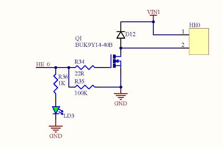
Schaltplan mit MOSFET und LED
VIN1, HE0, 1, 2, D12, Q1, BUK9Y14-40B, R34, 22R, R36, 1K, R35, 100K, GND, LD3, GND
in „Name dieser Art an Diodenschaltung“ · Analoge Elektronik und Schaltungstechnik · · Schaltpläne
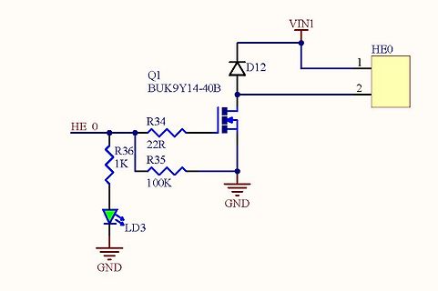
-
 Bild
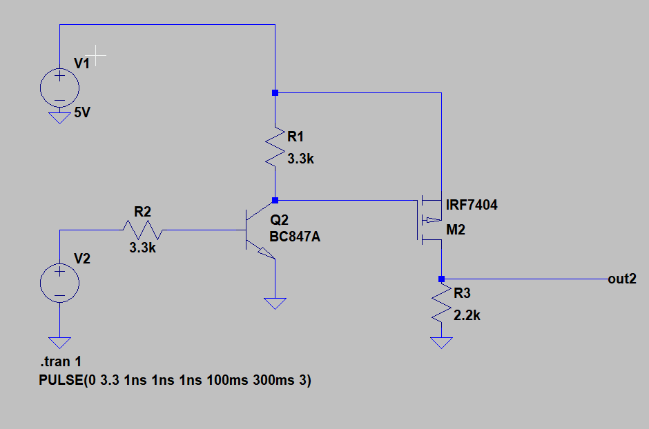
Schaltplan mit Transistor und MOSFET
V1 5V R1 3.3k Q2 BC847A R2 3.3k V2 IRF7404 M2 R3 2.2k out2 .tran 1 PULSE(0 3.3 1ns 1ns 100ms 300ms 3)
in „High Side Switch Mosfet“ · Analoge Elektronik und Schaltungstechnik · · Schaltpläne
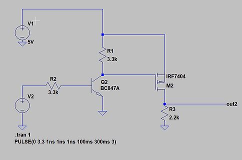
-
 Bild
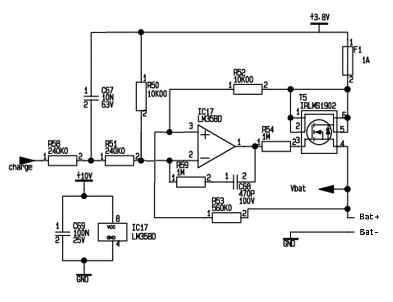
Schaltplan einer Ladeschaltung mit MOSFET
+3.8V F1 1A 2 R52 10K00 2 T5 IRLM1902 54 23 4 Vbat Bat + Bat - GND R58 240K0 R51 240K0 charge +10V C69 100N 25V IC17 LM358D 8 4 GND 1 2 C67 10N 63V 2 R50 10K00 2 3 2 1M R59 1M 2 1M C58 470P 100V R53 560K0 2 550K0 2
in „Ladeschaltung für 2x NiMH Zelle - wo passiert die Strombegrenzung“ · Analoge Elektronik und Schaltungstechnik · · Schaltpläne
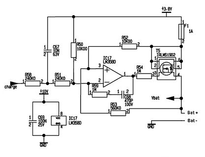
-
 Bild
Schaltplan mit MOSFETs und Widerständen
100 10k
in „Phasenanschnitt - Mosfet geht kaputt“ · Analoge Elektronik und Schaltungstechnik · · Schaltpläne
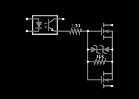
-
 Bild
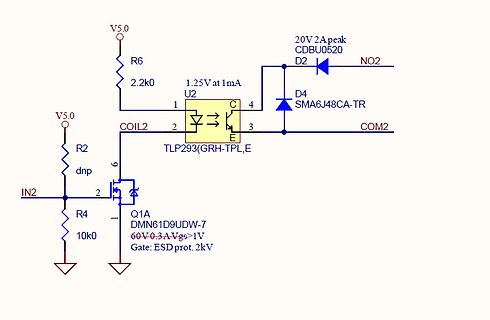
Schaltplan mit Optokoppler und MOSFET
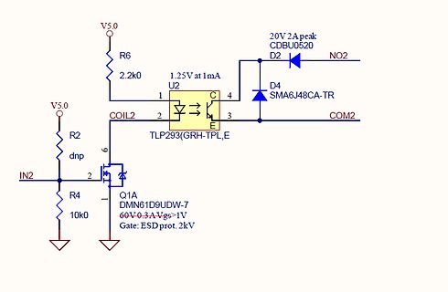
V5.0 R6 2.2k0 U2 1 2 3 4 1.25V at 1mA TLP293(GRH-TPL,E) COIL2 20V 2A peak D2 NO2 D4 SMA6J48CA-TR COM2 V5.0 R2 IN2 6 2 Q1A DMN61D9UDW-7 60V 0.3AVgs>1V R4 10k0 Gate: ESD prot. 2kV
in „24V Digitalausgang für Jetson Nano“ · Analoge Elektronik und Schaltungstechnik · · Schaltpläne
-
 Bild
Schaltplan mit Optokoppler und MOSFET
V5.0 R6 2.2k0 U2 1 2 3 4 1.25V at 1mA TLP293(GRH-TPL,E) COIL2 D2 20V 2A peak CDBU0520 NO2 D4 SMA6J48CA-TR COM2 V5.0 R2 IN2 6 2 Q1A DMN61D9UDW-7 60V 0.3AVgs>1V R4 10k0 Gate: ESD prot. 2kV
in „24V Digitalausgang für Jetson Nano“ · Analoge Elektronik und Schaltungstechnik · · Schaltpläne