setting with a step of 0.1V in the range of 2.0V to 6.0V is possible. Designation of Output Type: c A: Nch Open Drain C: CMOS Designation of Packing Type: d A: Taping C: Antistatic bag for TO-92 and samples Designation of Taping Type: Ex. TO-92: RF, RR, TZ SOT-89: T1, T2 e SOT-23-5: TR, TL (refer to
Screen Engine (CTSE) has the following features: • I C interface to Capacitive Touch Panel Module (CTPM) • Detects up to 5 touch points at the same time • Supports CTPM with Focaltech and Goodix touch controller. • Supports touch host mode. Please refer
von dessen Stromversorung miss den gleichen Strom. Ach nee, geht ja gar nicht, ist ja alles ein SoC hm...
Werbekampagne mit Paulchen Panther) marketingtechnisch völlig falsch behandelt. Auch mit den Compilern für C/C++ (Visual Age C++) hatte IBM damals definitiv die Nase vorn, was SW-Erstellung anbelangt (z.B. grafische Erstellung von Software mit Ereignisbehandlung über (grafische Verbindungen zwischen den Objekten
the antenna design guide and to the specific application notes for the reader IC. R1 1 OEMBoard 2 C1 LANT C3 5 C6 6 C5 C4 C8 C2 R2 6.1.3.3 Serial Interface The OEM Board can be connected directly with a micro controller. Alternatively the OEM Board also can be connected to most serial interface types
Adjustable version availabilityREF = 1.25 V) ■ Internal current and thermal limit ■ Available in ± 1 % (at 25 °C) and 2 % in full temperature range SOT-223 SO-8 ■ Supply voltage rejection: 75 dB (typ.) 25 °C. The adjustable LD1117 is pin to pin Description compatible with the other standard. Adjustable voltage
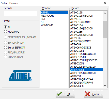
Hallo in das Forum. Wer könnte mir einen AT89C4051 flashen? HEX File vorhanden. Oder mir einen Programmer verkaufen bzw. leihen?
#7586078: > Der SP200S kann das. Gibts aus China für um die 10€. Der SP200S kann nur Atmel MCS-51 mit ISP: Beschreibung: Support MCS51 series of ATMEL Corporation and AVR MCU download Programming (ISP) (only support enhanced version) Der AT89C4051 kann KEIN ISP, von daher ist da ein AT89S4051
IMPORTANT NOTICE ****************************** A In order to avoid discharging the buffer battery for the C-MOS nemory with consequent 1oss of ca1ibrating data, it is reco'rımendedto operate the instrument with mains Poürer switched on for at least five hours every 6 ı months, thus recharging Ehe buffer battery
Cathode + 2 3 •Transistors 2N5401C-AT/P 2N5551C-AT 2SA1576A 2SA1695 O,P,Y 2SA1708 2SA1770S/T-AN 2SA949 2SA1015-Y 2SC4468 O,P,Y 2SC1815 Y 2SC2229 C E E B B B C B E C E C C E C E B C B B E 2SC1740S 2SC3906K 2SC4081 T106 2SC4614S/T-AN 2SC5938A
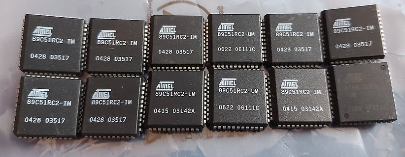
Hallo, noch 12St. gebrauchte geprüfte ATMEL AT89C51RC2 - PLCC44 abzugeben. (Waren alle gesockelt. Kein Lötzinn, sauber und keine verbogene Pins) Neu kosten die aktuell wahnsinnige 8€/St. https://www.mouser.de/ProductDetail/Microchip-Technology/AT89C51RC2-SLSUM?qs=scMUj%2FjL2g1JMgWj2dgv2g%3D%3D Alle für 13€ + 2,50€ Versand (Versand DHL/Post/ Hermes und Paypal) Bei Interesse bitte PM mit Artikelangabe. Danke! MFG Roger
Zähler cnt6 auf 0 ansonsten erhöhe den zähle cnt6 um 1 bekomme folgende Fehlermeldungen: [c]Error (10821): HDL error at AtariMainboardFPGA.vhd(150): can't infer register for "phi2short" because its behavior does not match any supported register model Error (10822): HDL error at AtariMainboardFPGA.vhd
RS-FF aus 2 NAND q2 <= clock7 nand q1; phi2sshort <= q1; end process; [/vhdl] [c]Error (10327): VHDL error at blink01.vhd(150): can't determine definition of operator ""nand"" -- found 0 possible definitions [/c]
.20 . B.3 Windows Multimedia Scancodes: . . . . . . . . . . . . . . . . . . . . . . . . . . . .20 C Keyboard Scancodes: Set 3 21 2 1 Die PS/2 Tastatur-Schnittstelle 1.1 Einleitung Dieser Artikel versucht alle Fragen rund um AT und PS/2 Tastaturen zu beleuchten. Er enthal Informationen ber die Low-Level-Signale
wave CH I 14) P2005: Variable balance CH I – Set all other controls to their midrange positions. 15) C2011/C2007: 10:1 Attenuator compensation CH I If different settings are required, it is specified in each adjust- 16) C2009/C2010: 100:1 Attenuator compensation CH I ment. 17) P2011: Y-Gain CH II at 5
8 8 8 51CN 51ACN 51CN−xx 51ACN−xx PAyy P−yy AWL AWL AWL AWL AYWG AYWG YYWWG YYWWG YYWWG YYWWG G G 1 1 1 1 1 1 xx = 3.0, 3.3, or 5.0 y = 3 or 5 yy = 30, 33, or 50 z = A or C A = Assembly Location WL, L = Wafer
Hallo, noch 12St. gebrauchte geprüfte ATMEL AT89C51RC2 - PLCC44 abzugeben. (Waren alle gesockelt. Kein Lötzinn, sauber und keine verbogene Pins) Neu kosten die aktuell wahnsinnige 8€/St. https://www.mouser.de/ProductDetail/Microchip-Technology/AT89C51RC2-SLSUM?qs=scMUj%2FjL2g1JMgWj2dgv2g%3D%3D Alle für 12€ + 1,60€ Versand (Versand DHL/Post/ Hermes und Paypal) Bei Interesse bitte PM mit Artikelangabe. Danke! MFG Roger
declarations). * Improved optimizations for code speed for stm8, pdk, z80 (and related). * New mos65c02 port to better support the WDC 65C02. Das umfassende ChangeLog findet sich unter: https://sourceforge.net/p/sdcc/code/HEAD/tree/tags/sdcc-4.4.0-rc1/sdcc/ChangeLog Philipp (SDCC 4.4.0 Release
kennen gelernt, als ich mit Mikrocontrollern überhaupt begonnen habe. AT89C51AC3 und Keil Demo Version war sch*****. Für den AC3 musste ich nur einen anderen 8051-Header anpassen. War wohl so um 2003-2005, also bald 20 Jahre.
0.5% ±0.5% ±0.5% LOAD REGULATION ±2.0% ±0.5% ±0.5% ±0.5% ±0.5% ±0.5% SETUP, RISE TIME 1000ms, 50ms at full load HOLD UP TIME (Typ.) 16ms/230VAC 16ms/115VAC at full load VOLTAGE RANGE Note.490 ~ 264VAC 127 ~ 370VDC FREQUENCY RANGE 47 ~ 63Hz POWER FACTOR (Typ.) 0.97/230VAC 0.98/115VAC at full load INPUT
for break event Processor Pending Break Event Indication C2, C3, C4 indication (See FERR# Mux Enable in GCS, Chipset Config Registers:Offset 3410h:bit 6) C2, C3, C4, Can be sent at any time after the Ack-C2 REQ-C0 Message from MCH C5, C6 message and before the Ack-C0 message, when not in C0 state. 5.13.5.1 Slow C4 and C5 Exit (Mobile Only) In order to eliminate the audible noise caused by aggressive voltage ramps when exiting C4 or C5 states at a regular, periodic
frequency fC. The first address byte can be at any location. The address is automatically increased to the next higher address after each byte data is shifted out, so the whole memory can be read out at a single
PXA320 Processor The Limestone PDA Baseboard is based on the Marvell XScale® PXA320 processor running at up to 806 MHz. The operating system and a large flash file system are stored in a 1GB NAND Flash device. Extension Connector On-Board Features 3xUART, SSP, I2C, Analog and Digital Audio I/O, Keypad,
110 dB SupplyVoltage Range ±5 ±16.5 ±5 ±16.5 ±5 ±16.5 V Supply Current 4 5 4 5 4 5 mA OUTPUTVOLTAGE, AT R L 2 kΩ TMINtoTMAX ±10 ±10 ±10 V Output Short-Circuit Current 25 25 25 mA TEMPERATURE RANGES N Package 0 70 0 70 °C D Package −25 +85 −25 +85 −55 +125 °C 1 2Ifone terminal ofeach differential channel
Beitrag #7557116: > Michael schrieb: >> Ich war sehr froh als der 8051 rauskam > > Für mich war der 89C2051 der erste Mikrocontroller, an dem ich wirklich > Freude hatte. Davor fand ich den Eigenbau von Schaltungen mit > Mikrocontroller einfach nur anstrengend. Ja. Der uC ist die Mikroprozessor-LP
> NEIN, ihr dürft auch keinen ISP benutzen, denn der olle 8051 hatte das > auch nicht. Bei den AT89C51RC2 verwendete ich früher mal auch selbstverständlich den Serial ISP oder auch den ASIX ISP Daß mir 8-bitter immer noch wegen ihrer Gutmütigkeit und Einfachheit gefallen, sollte kein Verbrechen
U s r s R32C/152 Group User’s Manual: Hardware M a u a l R32C/152 Group 32 User’s Manual: Hardware RENESAS MCU M16C Family / R32C/100 Series represents information on the product at the time of publication and is
, CS1, and RES. Data Modul AG - www.data-modul.com 10 5.2 Timing Specifications Reset Input Timing At Ta = -20 °C to +70 °C, VDD = +3.3V±5%, VSS = 0V. Table 6 Figure 3: Reset Timing Diagram System Buses Read/Write Characteristics (for 8080 Series MPU) At Ta = -20 °C to +70 °C, VDD = +3.3V±5%, VSS = 0V
not necessarily in ascending order. EXAMPLE 1 An expanded memory board has its page frame starting at address C0000h and has no mappable conventional memory. For this configuration, physical page 0 corresponds to segment address C000h, physical page 1 corresponds to segment address C400h, etc. The array would contain the following data (in this order): C000h, 00h C400h, 01h C800h, 02h CC00h, 03h EXAMPLE 2 96 An expanded memory board has a large page frame starting at address C0000h and has mappable conventional memory from 90000h through 9FFFFh. For
TP=200/SPAN 4040 N1(0)=-B2/1000 :N2(0)=B2/1000 :N3(0)=0 4050 FOR I=1 TO 20 4060 ATT=-I*10+200 4070 AT01=N1(I-1)*TP+100 4080 AT1=N1(I)*TP+100 4090 AT02=N2(I-1)*TP+100 4100 AT2=N2(I)*TP+100 4110 AT03=(AT01+AT02)/2 4120 AT3=(AT1+AT2)/2 4130 IF N1(I)<0 THEN 4170 4140 IF N3(I-1)=0 THEN AT01=DUMMY :AT1=DUMMY :GOTO 4170 4150 AT1=N3(I)*TP+100 4160 AT01=N3(I-1)*TP+100 4170 LINE (AT01,ATT+10)-(AT1,ATT) 4180 LINE (AT02,ATT+10)-(AT2,ATT) 4190 IF N4(I)>0 THEN LINE (AT03,ATT+10)-(AT3,ATT),,,&HCCCC 4200 NEXT I 4210 LINE (0,UA*2+200
noted Supply possible. Caen fire part. 277 TDA8703T/C4 TDA8703T D CONVERTERS (CAEN) 935020320118 T S 3 20-nov-04 20-feb-05 None noted Supply possible. Caen fire part. 278 TDA8708AT/C1 TDA8708AT D CONVERTERS (CAEN) 935063030112 T S 3 20-nov-04 20-feb-05 None noted Supply possible. Caen fire part. 279 TDA8708AT/C1 TDA8708AT D CONVERTERS (CAEN) 935063030118 T S 3 20-nov-04 20-feb-05 None noted Supply possible. Caen fire part. 280 TDA8709AT/C2 TDA8709AT D CONVERTERS (CAEN) 935075380112 T S 3 20-nov-04 20-feb-
110 SDA Out TABLE 1-3: I C BUS DATA REQUIREMENTS I C Interface AC Characteristics: Unless otherwise noted, 1DDV 5.5V at -40C AT +125C,PU (SCL, SDA) = 1 k, L (SCL, SDA) = 135 pF Param. No. Characteristic Sym. Min. Typ. Max
3.9. The normal operation range of the batteries is defined by the battery management system (BMS). At SoC = 100%, the maximum battery voltage is V batt,max= 57V, at SoC = 20% the nominal battery voltage is Vbatt,nom= 51.2V, and at SoC = 0% the minimum battery voltage is V batt,min= 44.6V (the battery
. If Xs, Marker 1 and/or Marker 2 are chosen, the Xs value will be shown with a corresponding L or C value at the marked frequency. Text written in the free text area will be shown in the screenshot picture as well as on the graphics captured by the clipboard. It's possible to make screenshot manually
but not tested. † Data in the Typical (“Typ”) column is at 5V, 25°C unless otherwise stated. These parameters are for design guidance only and are not tested. Note 1: To ensure these oscillator frequency tolerancDD,and VSS must be capacitively decoupled as close
> Bestimmt hat jemand da eine Bauteilbezeichnung parat? Nö. Seit ich Flash-MCs benutze (1993: AT89C2051), brauche ich keine zusätzlichen HW-Decoder. Auf dem 80C51 sind das gerade mal 20 Byte Code (MOV DPTR + MOVC + 16 Byte Tabelle. Du kannst Dir ja nen ATtiny24 als Dekoder programmieren.
Peter D. schrieb im Beitrag #7529046: > 1993: AT89C2051 Ich erinnere mich. Der hatte einen schön übersichtlichen Assembler Befehlssatz.
1st Initialisation Time after programmed sector [INI_TIMEOUT_AP: 0x0a] Power class for 52MHz, DDR at 3.6V [PWR_CL_DDR_52_360: 0x00] Power class for 52MHz, DDR at 1.95V [PWR_CL_DDR_52_195: 0x00] Power class for 200MHz at 3.6V [PWR_CL_200_360: 0x00] Power class for 200MHz, at 1.95V [PWR_CL_200_195: 0x00
1st Initialisation Time after programmed sector [INI_TIMEOUT_AP: 0x0a] Power class for 52MHz, DDR at 3.6V [PWR_CL_DDR_52_360: 0x00] Power class for 52MHz, DDR at 1.95V [PWR_CL_DDR_52_195: 0x00] Power class for 200MHz at 3.6V [PWR_CL_200_360: 0x00] Power class for 200MHz, at 1.95V [PWR_CL_200_195: 0x00
.......................................................................... 62 5.1.1 Installing the C251 Compilation Environment........................................................ 62 5.1.2 How to Install Keil's C51, C251, and MDK at the Same Time............................... 65 5.2 Adding Models
are shown in millimeters (inches) Y DIMENSIONS 6 M D 5 O MILLIMETERS INCHES L MIN MAX MIN MAX A 0.89 1.12 .036 .044 A1 0.01 0.10 .0004 .0039 A2 0.88 1.02 .035 .040 3 6 b 0.30 0.50 .0119 .0196 E E1 c 0.08 0.20 .0032 .0078 1 2 ccc C B A D 2.80 3.04 .111 .119 E 2.10 2.64 .083 .103 E1 1.20 1.40 .048 .055
Testing and measurement techniques. Section 13: Harmonics, interharmonic including mains signalling at A. C. Power port, Immunity tests. r630005d - 16.10.aa – Dieter Helmich Seite 83 von 122 5.9 Checking the level of supplied power If the user wishes to reactivate the booster, this can be done. The booster

 Bild
Bild
 Bild
Bild