dein N!N1 hat 16 Ausgänge frei. Da 16 einzelne Überstromüberwachungen aufwändig sind, smart low side switches wie BD8LD650 teuer, würde ich einen einzelnen Widerstand in alle zusammengefassten Transistormasseverbindungen einschleifen (z.B. 16 x 0.5A = 8A, 0.05 Ohm macht 0.4V) und den Spannungsabfall
. schrieb im Beitrag #7956765: > Da 16 einzelne Überstromüberwachungen aufwändig sind, smart low side > switches wie BD8LD650 teuer, würde ich einen einzelnen Widerstand in > alle zusammengefassten Transistormasseverbindungen einschleifen (z.B. 16 > x 0.5A = 8A, 0.05 Ohm macht 0.4V) Was meinst
Der Strom fließt den Weg zurück über einen der Low-Side MOSFETs und einen Shunt zu GND. Die Totzeit macht der Treiber automatisch. Wenn Du den nicht verwendest musst Du natürlich eine Totzeit selbst einbauen. Es sind sechs MOSFETs im Schaltplan, nicht drei. Es wird immer nur ein High-Side- und ein Low-Side-MOSFET geschalten. Viel Spaß beim grillen. https://www.youtube.com/watch?v=xMvSgjFHJbg
DESCRIPTION Pin Name Description 1 GND Negative Main Supply 2 VDD +15 V Main Supply 3 HINU Logic Input High Side Gate Driver - Phase U 4 HINV Logic Input High Side Gate Driver - Phase V 5 HINW Logic Input High Side Gate Driver - Phase W 6 LINU Logic Input Low Side Gate Driver - Phase U 7 LINV Logic Input Low Side
Diagram www.onsemi.com 3 NFAQ1060L33T Table 1. PIN FUNCTION DESCRIPTION Pin Name Description 1 VSS Low−Side Common Supply Ground 2 VDD Low−Side Bias Voltage for IC and IGBTs Driving 3 HIN(U) Signal Input for High−Side U Phase 4 HIN(V) Signal Input for High−Side V Phase 5 HIN(W) Signal Input for High−Side
Block Diagram www.onsemi.com 3 NFAQ1560R43T PIN FUNCTION DESCRIPTION Pin Name Description 1 VSS Low−Side Common Supply Ground 2 VDD Low−Side Bias Voltage for IC and IGBTs Driving 3 HIN(U) Signal Input for High−Side U Phase 4 HIN(V) Signal Input for High−Side V Phase 5 HIN(W) Signal Input for High−Side
Thermistor 17 NU Low−side Emitter Connection − Phase U 18 NV Low−side Emitter Connection − Phase V 19 NW Low−side Emitter Connection − Phase W 20 W Phase W Output / High−side Floating Supply Offset Voltage 22 VBW High−side Floating Supply Voltage − Phase W 26 V Phase V Output / High−side Floating Supply Offset Voltage 28 VBV High−side Floating Supply Voltage − Phase V 32 U Phase U Output / High−side Floating Supply Offset Voltage 34 VBU High−side Floating Supply Voltage − Phase U 38
view taped, 1190 pcs/reel to infrared bursts at 940 nm. The frequency of the burst TSSP960..TR - side view taped, 1120 pcs/reel should correspond to the carrier frequency shown in the parts table. This component has not been qualified according to APPLICATIONS automotive specifications. • Reflective
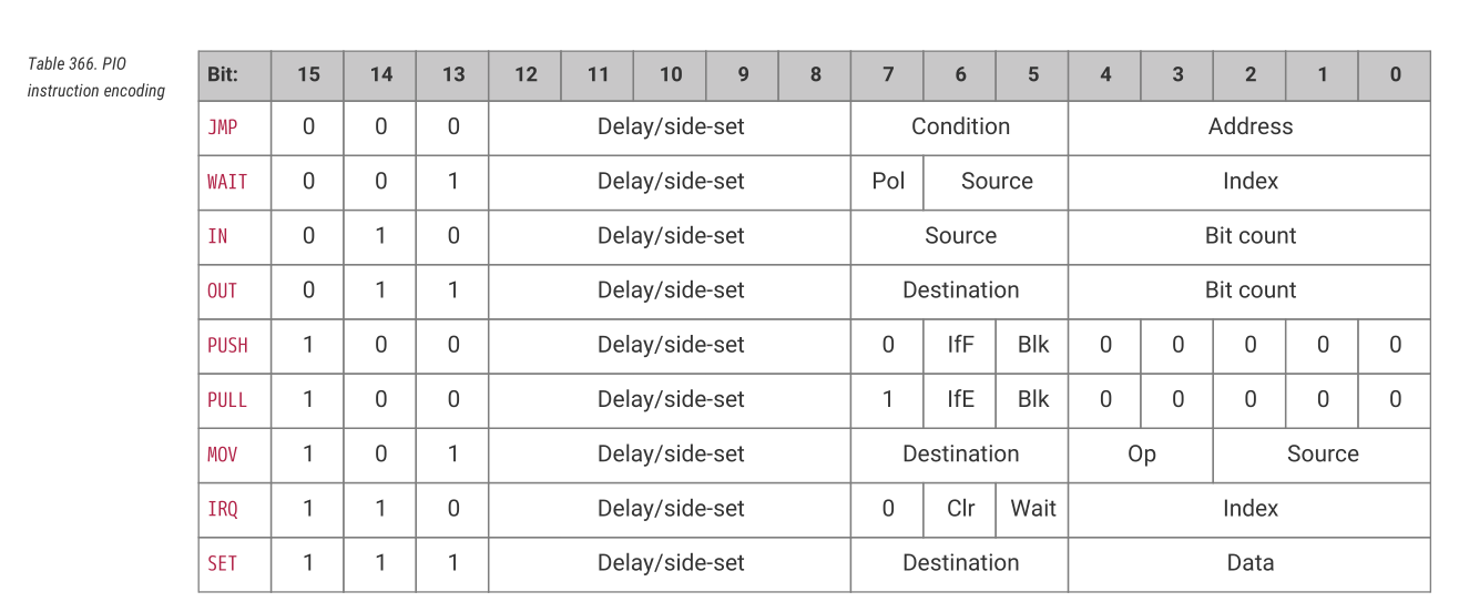
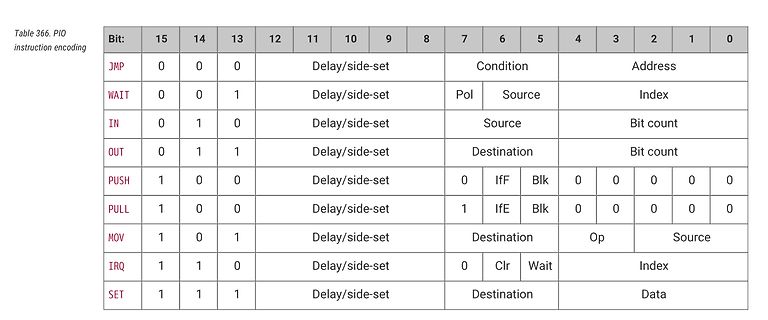
pseudoinstruction, as a convenience: nop Assembles to mov y, y . "No operation", has no particular side effect, but a useful vehicle for a side-set operation or an extra delay.[/pre]
Q1028 C6 Q1085 C6 Q1029 H5 Q1086 B6 7 Q1030 G5 Q1031 F5 65 A B C D E F G H I J RX-V4A/TSR-400 1 (Side A) (Side A) (Side A) AMP (2) AMP (3) AMP (4) 2 CB115 3 W112 N . R D + 1 M T DIGITAL 4 (CB23) 5 6 7 66 A B C D E F G H I J RX-V4A/TSR-400 1 AMP (2) (Side B) AMP (3) (Side B) AMP (4) (Side B) 2 3 4 5
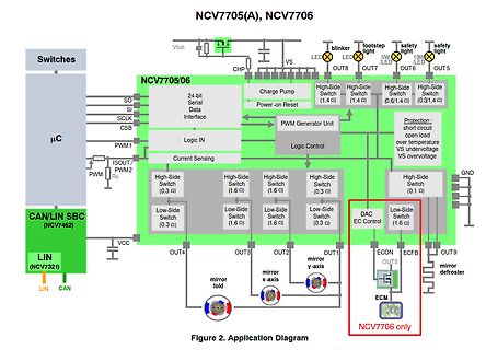
Guten Abend, ich plane eine Neu-Baugruppe, die u.a. simple Low-Side Ausgänge zur Verfügunge stellen soll. Das bisherige Modul hat mehrere ULN2804 Chips als Ausgangstreiber an Parallel-Ports vom µC dafür verwendet, das war völlig OK für den Use-Case. Für die überarbeitete
Ansteuerung. IRLML6402 (P-Kanal) oder IRML2502 (N-Kanal) wären da zum Beispiel genannt, wenn es Low-Side sein muss. Ein leistungsfähiger Treiber sind die automotive High-Side Schalter ITS711L1 bzw. BTS711L1 (jeweils 4 Ausgänge), sind aber aufgrund geringer Anstiegsrate nicht für PWM geeignet. Vielleicht
17 V Average Forward Current IF(AV) 50 A Half cycle sine-wave, Surge Forward Current IFSM positive side, 10ms, 1 shot. 500 A Nonrepetitive Peak Reverse Voltage V RSM 1 shotseeFigure 1. 70 V Junction Temperature T J −40 to 235 °C Case Temperature T C See Figure . −40 to 215 °C Storage Temperature T STG
family of equations, Eqs. 2.5-3, shows that each contains a current or a voltage on the right-hand side. However, that parameter is defined in the next equation above. A continued substitution will eventually terminate at the input voltage which was defined.The result is (2.5-4) This method appears formidable
may have a vast range, depending on the used MOS-FET, e.g. down to 2 Volt at the “Lower voltage” side and up to 10 Volt or more at the “Higher voltage” side of the level shifter. An additional function of the level shifter is that it can isolate a powered-down section in a bus system, without obstructing
Bedienelemente usw. für alte Technik sucht... https://forum.zerspanungsbude.net/viewtopic.php?f=16&t=87577&sid=dc8b859c439ddefdc43b98cf005b4d22 Grüße Bernd
Client to initiate a transaction, A MODBUS Indication is the Request message received on the Server side, A MODBUS Response is the Response message sent by the Server, A MODBUS Confirmation is the Response Message received on the Client side The MODBUS messaging services (Client / Server Model) are used
panel or a PC, which implements an RS232 Data Terminal Equipment. ITr Physical bus Interface on Trunk side. IDv Physical bus Interface on Derivation (or tap or device drop) side. LT Line Termination. MODBUS Device a Device that implements MODBUS over Serial Line and respects this Technical Note. RS232 EIA
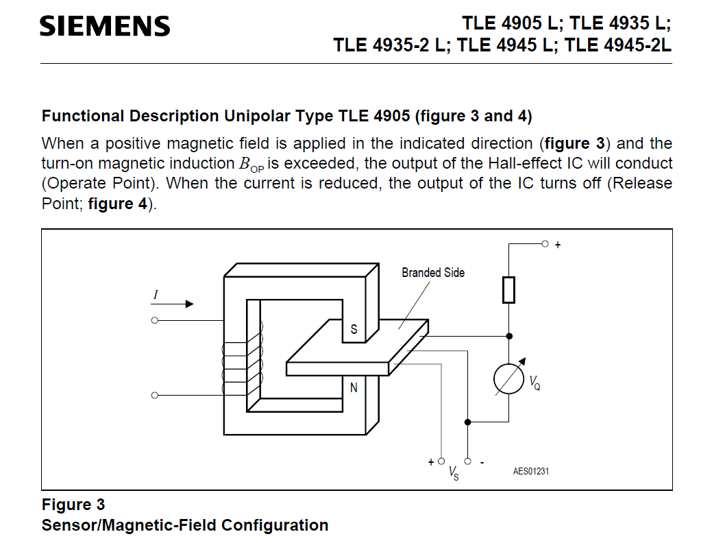
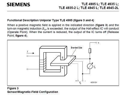
). When the current is reduced, the output of the IC turns off (Release Point; figure 4).
Branded Side
S
N
+
+
-
VO
VS
AES01231
Figure 3
Sensor/Magnetic-Field Configuration
ich zudem in jedem Mux Zyklus eben schnell eine Zeile Tasten abchecke bevor ich die nächste High-Side der "Spalte" aktiviere...augenscheinlich ist es wohl so geplant dass man ein Bit auf dem 8-Bit Bus durchlaufen lässt und dann jeweils bei Pin 13 (T1) schaut ob die Taste gedrückt ist...
insured with isolated interconnections. a second PIN photodiode (pins 5, 6) located on the output side These isolated interconnections commonly use isolation ampli- of the coupler.The output current, IP2, from this photodiode fiers. accurately tracks the photocurrent generated by the servo pho- todiode
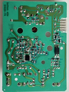
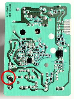
Da wird wohl der High-Side-Schalter durchlegiert sein. Das Modul scheint man ja öffnen zu können, evtl lässt sich der defekte Chip austauschen.
H. H. schrieb im Beitrag #7940138: > Da wird wohl der High-Side-Schalter durchlegiert sein. Das Modul scheint > man ja öffnen zu können, evtl lässt sich der defekte Chip austauschen. Wenn das so wäre, ist den der Effekt das der Schalter eine Masseverbindung
, sogar auf Ausnutzung von Bugs des SID > (Sounderzeugung durch Änderungen des Lautstärke-Registers). Mit SIDs kann man schon interessante Klänge erzeugen. Je mehr* SIDs, umso beeindruckender das Ergebnis. Es können auch /emulierte
. Der Hüllkurvenformer (aka ADSR+VCA) ist ein Added-Bonus. Genauso der VCF. Die emulierten SIDs sind nichts anderes als /gesamplete/ SIDs (PAL/NTSC/SID-Derivate) und einer GigaSampler-Engine unten drunter. Als Einzelstimme ist gegenüber einem SID auch /kein/ Unterschied auszumachen. Sie ist
AND DIMENSIONS APPLY SOLDER MASK TO AREAS THAT ARE NOT SOLDERED 4.00 ±0.10 R = 0.115 0.40 ± 0.10 (2 SIDES) TYP 7 12 R = 0.05 TYP 3.30 ±0.10 3.00 ±0.10 PIN 1 (2 SIDES) 1.70 ± 0.10 TOP MARK PIN 1 NOTCH (NOTE 6) R = 0.20 OR 0.35 × 45° (UE12/DE12) DFN 0806 REV D 6 1 0.200 REF 0.75 ±0.05 0.25 ± 0.05 0.50 BSC
operation. The weight of the sensor is approx. 0.6 g. Figure 3: Sensor package dimensions of SCD4x: top, side and bottom view (left to right, projection method 1). All dimensions in millimeters. 4.2 Land Pattern Recommendation Recommended land pattern, solder paste, and solder mask are shown in Figure 4. The
single-ended amplifier configura- In order to reduce power consumption while not in use, the tion where one side of its load is connected to ground. LM9022 contains a shutdown pin to externally turn off the A bridge amplifier design has a few distinct advantages over amplifier’s bias circuitry. This shutdown feature
peak-detection genutzt habe fehlt aus Lizenzgründen. Kannst du aber mit browserify in ein browser-side slayer.js umwandeln wie ich es gemacht habe). Das kannst du dann mit allen chrome basierten browser (Chrome, Chromium, Edge, Brave, ...) öffnen (musst eigentlich nur das index.html im browser öffnen
Proceeding: REAR MOLD PANEL (1) Remove the screws. ↑Shooting direction: A↑ View from the bottom 15 2. SIDE PANEL Proceeding: REAR MOLD PANEL → SIDE PANEL (1) Remove the screws. Front side STEP1 STEP1 STEP2 STEP2 TOP SIDE TOP SIDE View from the bottom 3. TOP PANEL ASSY Proceeding: REAR MOLD PANEL → SIDE PANEL
installing a battery in a device, make sure that the positive terminal is facing up, or at least to the side. As this battery uses Battery Battery liquid thionyl chloride as the positive active material, placing the positive terminal at the bottom will cause the thionyl chloride to become maldistributed, which
defined, C programs can use names like <tt>PORTA</tt> directly in C expressions (also on the left side of assignment operators) and GCC will do the right thing (use short I/O instructions if possible). The \c __SFR_OFFSET definition is not used in any way in this case. Define \c _SFR_ASM_COMPAT as 1
der zu erwarten ist. Bei Einspritzungen ohne den falschen Peak fällt die Spannung auf der Low-Side Leitung e-förmig ab wie zu erwarten. Gemessen hab ich beide Leitungen gegen Masse und dann im Oszilloskop Low-Side von High-Side abgezogen. Strom mit Stromtastkopf. Gemessen hab ich bei Leerlauf
Bilder angehängt. Einmal Spannung mit regulärem Verlauf, einmal Spannung mit Peak. Blau ist High-Side, Rot Low Side, Violett die Differenz und damit die am injektor anliegende Spannung, sowie Grün der Strom durch den Injektor. Darüber hinaus sind nochmal die Ströme einzeln aufgezeichnet. Die Frage
hier z.B einen doppelten Switch: https://www.reichelt.de/de/de/shop/produkt/power_switch_high_side_usb_active_low_so-8-386821 Keine Ahnung ob die auch einen einzelnen haben. Musst du halt selber mal suchen. Vanye
nennt sie Load > switch. In Zeiten der Halbleiterkrise mußte ich leider merken, daß bei High-Side Treibern jeder Hersteller sein eigenes Süppchen kocht, bezüglich Verhalten, Pinbelegung und Footprint. Es gibt keinen Standard. Ich bin daher wieder auf einzelne MOSFETs zurück. SOT-23 bleibt eben
firm. ● When climbing up the ladder, keep your body stable and your center of gravity between the side rails, and do not overreach to the sides. ● When a step ladder is used, ensure that the pull ropes are secured. ● If a single ladder is used, the recommended angle for the ladder against the floor is

 Bild
Bild
 Bild
Bild
 Bild
Bild
 Bild
Bild
 Bild
Bild
 Bild
Bild
 Bild
Bild
 Bild
Bild
 Bild
Bild
 Bild
Bild
 Bild
Bild
 Bild
Bild
 Bild
Bild
 Bild
Bild
 Bild
Bild
 Bild
Bild