-
PDF
ir2110.pdf
supply return VCC Low side supply LO Low side gate drive output COM Low side return 4 www.irf.com IR2110(-1-2)(S)PbF/IR2113(-1-2)(S)PbF LeadAssignments 14 Lead PDIP 16 Lead SOIC (Wide Body) IR2110/IR2113 IR2110S/ IR2113S 14 Lead PDIP w/o lead 4 14 Lead PDIP w/o leads 4 & 5 IR2110-1/IR2113-1 IR2110-2
in „IR2110 Probleme“ · Mikrocontroller und Digitale Elektronik ·
-
PDF
ir2110.pdf
supply return VCC Low side supply LO Low side gate drive output COM Low side return 4 www.irf.com IR2110(-1-2)(S)PbF/IR2113(-1-2)(S)PbF LeadAssignments 14 Lead PDIP 16 Lead SOIC (Wide Body) IR2110/IR2113 IR2110S/ IR2113S 14 Lead PDIP w/o lead 4 14 Lead PDIP w/o leads 4 & 5 IR2110-1/IR2113-1 IR2110-2
in „Wechselrichter mit MOSFET Endstufe“ · Analoge Elektronik und Schaltungstechnik ·
-
PDF
ir2110.pdf
supply return VCC Low side supply LO Low side gate drive output COM Low side return 4 www.irf.com IR2110(-1-2)(S)PbF/IR2113(-1-2)(S)PbF LeadAssignments 14 Lead PDIP 16 Lead SOIC (Wide Body) IR2110/IR2113 IR2110S/ IR2113S 14 Lead PDIP w/o lead 4 14 Lead PDIP w/o leads 4 & 5 IR2110-1/IR2113-1 IR2110-2
in „HIGH AND LOW SIDE DRIVER Io+ Ausgangsstrom“ · Mikrocontroller und Digitale Elektronik ·
-
PDF
IR2110-DataSheet.pdf
VCC Low side supply LO Low side gate drive output COM Low side return 4 www.infineon.com/gatedriver IR2110(S)PbF/IR2113(S)PbF LeadAssignments 14 Lead PDIP 16 Lead SOIC (Wide Body) IR2110/IR2113 IR2110S/IR2113S Part Number www.infineon.com/gaedriver 5 IR2110(S)PbF/IR2113(S)PbF Vcc=15V HV = 10 to 500V/600V
in „Inverter DC/AC mit EGS002 China DEV-Board“ · Analoge Elektronik und Schaltungstechnik ·
-
PDF
an-978_Bootstrap.pdf
the level of undershoot is still considered too high, then some reduction of dv/dt may be necessary. IR2110 PC BOARD KIT R3 D1 1N2074A Externalsnubbingand/or increasing gate drive re- V 9 Q1D sistance may be used to +15V DD V 6 Q 100V tradeefficiencyforlower VDD B C IRF740 0.47 switching rate. If the IR2110
in „IR2184 half bridgde driver / Ist PWM-Signal begrenzt?“ · Mikrocontroller und Digitale Elektronik ·
-
PDF
an-978.pdf
the voltage differential measured between the gate pin of the power MOSFET and the drive pin of the IR2110 during a fast transient was in excess of 2 V. Spike across freewheeling diode Spike at VS pin of IR2110 Figure 8: Q1 Turning Off a 20 A Inductive Load (20 ns / div and 20 V / div) 100 Turn-off time
in „Treiber-IC Peripherie berechnen“ · Mikrocontroller und Digitale Elektronik ·
-
PDF
an-978.pdf
the voltage differential measured between the gate pin of the power MOSFET and the drive pin of the IR2110 during a fast transient was in excess of 2 V. Spike across freewheeling diode Spike at VS pin of IR2110 Figure 8: Q1 Turning Off a 20 A Inductive Load (20 ns / div and 20 V / div) 100 Turn-off time
in „Isolierter High-Side Mosfet Treiber“ · Analoge Elektronik und Schaltungstechnik ·
-
PDF
ir2110-app-note.pdf
the voltage differential measured between the gate pin of the power MOSFET and the drive pin of the IR2110 during a fast transient was in excess of 2 V. Spike across freewheeling diode Spike at VS pin of IR2110 Figure 8: Q1 Turning Off a 20 A Inductive Load (20 ns / div and 20 V / div) 100 Turn-off time
in „[Transistor Ansteuerung] Ausgang kein Rechteck?“ · Analoge Elektronik und Schaltungstechnik ·
-
PDF
an-978.pdf
the voltage differential measured between the gate pin of the power MOSFET and the drive pin of the IR2110 during a fast transient was in excess of 2 V. Spike across freewheeling diode Spike at VS pin of IR2110 Figure 8: Q1 Turning Off a 20 A Inductive Load (20 ns / div and 20 V / div) 100 Turn-off time
in „high-side gate driver mit LT-Spice simulieren“ · Analoge Elektronik und Schaltungstechnik ·
-
PDF
an-978.pdf
the voltage differential measured between the gate pin of the power MOSFET and the drive pin of the IR2110 during a fast transient was in excess of 2 V. Spike across freewheeling diode Spike at VS pin of IR2110 Figure 8: Q1 Turning Off a 20 A Inductive Load (20 ns / div and 20 V / div) 100 Turn-off time
in „Halbbrücke Gate-Treiber Erklärung“ · Analoge Elektronik und Schaltungstechnik ·
-
PDF
an-978.pdf
the voltage differential measured between the gate pin of the power MOSFET and the drive pin of the IR2110 during a fast transient was in excess of 2 V. Spike across freewheeling diode Spike at VS pin of IR2110 Figure 8: Q1 Turning Off a 20 A Inductive Load (20 ns / div and 20 V / div) 100 Turn-off time
in „H-Brücke mit 100% Duty-Cycle“ · Analoge Elektronik und Schaltungstechnik ·
-
Datei
IR2110.txt
level abstract behavioral PSPICE model has been developed to simulate the electrical performance of IR2110 driver. The model can be used in Pspice version 8 or later (MicroSim Pspice). The IR2110 package includes three files: 1. Pspice subcircuit model file (IR2110.sub) 2. Symbol file (IR2110.slb) 3. Instruction file (IR2110.txt) The subcircuit model can be called directly in a plain Pspice netlist or more user friendly pspice schematics. To use the subcircuit model within a netlist,simply copy and paste the sub- circuit
in „Infineon PSpice Lib in LtSpice einbinden“ · Mikrocontroller und Digitale Elektronik ·
-
PDF
EG8010_datasheet.pdf
....................................... 9 6.5 EG8010+IR2110SSinusoid inverter (bipolar modulation) .................................................................... 9 6.6 EG8010+IR2110S Sinusoid inverter (low power frequency transformer) ..............
in „Inverter DC/AC mit EGS002 China DEV-Board“ · Analoge Elektronik und Schaltungstechnik ·
-
PDF
engine_driver_v08_brd.pdf
, 7,9C C 4 4 R5 Z 5 10 1 Q $ IR2110 3 U n R MAX662CPA 0 2 I C 0 2 1 C 0 I 1 C 4 0 01 D 0 220n 220n I n 42 4C 0 0 C U 1 C1 C2 1 u 0 26 C Z 6 3 210 1 Q U 1 C3 3 2 IC9 I C 100n 8 6 1 / 1 G 8 1Q / R 4 R7 R1 0 Q $ / IR2110 10 7 U 0 8 100k
in „Problem mit BLDC Schaltung“ · Analoge Elektronik und Schaltungstechnik ·
-
PDF
BLDC.pdf
D M SD SD S INFINIONTO263 12 3 LSB d LB LIN VCC 12V p S 13 1 VSS LO LSB COM 2 V IR2110D 1 GND GND GND r cr V S 0 r 6 IC3 e 6 S 3 0 VB 8 D 1 R 8 9 7 n U C R 5V VDD HO HSC 0 2 U 3 0 M HSCDOM 10 5 C 6 S HC HIN VS HSC INFI1IONTO263 O P S SD 11 SD 1 8 PC R LC 12 LIN VCC 3 12V L U LSCD M S 13 VSS LO 1 LSC INFINIONTO263 LSC r S 2 COM IR2110D GND GND GND 31.01.2017 22:18 f=1.70 C:\Users\Dani PC\Documents\eagle\BLDC Controll\LeistungsstufeV3.sch (Sheet: 1/1)
in „BLDC Halbbrücken nerven“ · Analoge Elektronik und Schaltungstechnik ·
-
PDF
BLDCv4.pdf
3 V D6 r LIN VCC pD 47 LSA LSA LSA S +C8 470µ 470µ 470µ 13 1 R2 d VSS LO p S 10µ COM 2 GND GND GND IR2110D C GND C GND V d VDD pi S +C18 + C17 + C16 C15 C14 C13 d 47 pi IC2 S 4 10µ 10µ 10µ D R7 1µ 1µ 1µ VB 6 7 DSpiceSpiceOrder 1 HS4 HS5 HS6 HS7D r +C6 S VDD 9 VDD HO 7 C4 GND GND GND GND GND GND HB HB
in „BLDC Halbbrücken nerven“ · Analoge Elektronik und Schaltungstechnik ·
-
PDF
engine_driver_v08.pdf
Sensoren 13 VSS R3 GND IRF3710Z + 14 VCC PC5(ADC5/SCL) 28 100n LO 1 X2-3 10 r 8 9 PB6(XTAL1/TOSC1) IR2110 t 7 10 2 X4-1 o GND OUT PB7(XTAL2/TOSC2) PD0(RXD) 3 RX MKDSN1,5/2-5,08 V PD1(TXD) 4 TX X4-2 8 8 PD2(INT0) 5 LIN3 MKDSN1,5/2-5,08 GND 4 GND GND GND PD3(INT1) 6 LIN2 OC2B 48V Motor + 7 PD4(XCK/T0)
in „Problem mit BLDC Schaltung“ · Analoge Elektronik und Schaltungstechnik ·
-
PDF
classd.pdf
DIS 7 1 4 5 6 R 2 3 IC2A n 5 IC2B 5 C1 CV THR C2 1 4 0 7 1 IC3A P$8 6R2 + 6R2 P$8 1 8 2 2 C 1 6 3 IR2110SHO HO IR2110S 100n GND V+ + 1n NE5532D NE5532D 2 2 P$7 Q2 Q42 P$7 2 TLC555 3 n 2 4093D + VB 4,7u 0 IRFR1205 IRFR1205 0 4,7u VB + 2,4k C 1 + P$11 P$6 3 3 P$6 P$11 GND R2 3 3 VDD VS C6 1 U u 0 U 2
in „Class D - so machbar?“ · Analoge Elektronik und Schaltungstechnik ·
-
PDF
Klasse_D.pdf
+24V X1-2 +12V X1-1 GND +24V 100n C16 +12V 1 _ 100n GND S 6 IR2110 HO P7 B 1N4148DO35-7 C6 U D4 M 22R P9 VDD VB P6 GND R15 IRFI4212TO220-5 H3 C5 + P10 HIN VS P5 + 5 +12V MOUNT-PAD-ROUND3.2 µ 9 4 G1 1 10u 4 C D H2 P11 SD G1/S2 3 X2-1 MOUNT-PAD-ROUND3.2 2 H1 P12 P3
in „50Hz Brummen bei Klasse D Endstufen“ · Mikrocontroller und Digitale Elektronik ·
-
PDF
Klasse_D.pdf
+24V X1-2 X1-1 +12V GND +24V 100n C16 +12V 5 1 1 0 100n GND A 6 IR2110 HO P7 B RN4148DO35-7 C6 U D4 M 22R P9 VDD VB P6 GND R15 H3 C5 + P10 P5 + 5 IRFI4212TO220-5 +12V MOUNT-PAD-ROUND3.2 HIN VS 7 9 4 P 1 10u µ C G1 D J H2 P11 4 3 22u SD G1/S2 X2-1 MOUNT-PAD-ROUND3.2
in „Verstärkung Audio Endstufe“ · Analoge Elektronik und Schaltungstechnik ·
-
PDF
classd2.pdf
3 IC3A IC2A IC2B IC2C 3 D3 5 1N4148 A 1 13 12 R3 11 10 9 8 2 e P$8 6R2 T1 + T3 6R2 P$8 0 C 2 4070D IR2110SHO IRFR1205 IRFR1205 HO IR2110S 4 LM393D 74HC14D 1k100p 74HC14D 74HC14D 2 P$7 R8 R12 P$7 2 A 5 IC6B + VB 4,7u 0 0 4,7u VB + C4 k 1 4 P$11 P$6 3 3 P$6 P$11 GND 3 R 6 e VDD VS C6 1 U u 0 U 2 C8 VS
in „Class D - so machbar?“ · Analoge Elektronik und Schaltungstechnik ·
-
PDF
Verstaerker.pdf
24V + UB-1 GND 100n 2 100n 100n +C17 GND C23 C24 C16 10µ +12V 7 n 1 2 0 1 _ F GND C 1 GND V 0 1N4004 IR2110 P7 B 1N4148DO35-7 D5 HO R D3 U Q1 7810!! M 22R IRF540 7818TV GND P9 VDD VB P6 n V 1 0 R15 1 VI VO 3 0 C 1 + P10 HIN VS P5 100n GND 100n 2 C22 C21 P11 SD P12 P3 GND LIN VCC Q2 IRF540 6 9 P13 P2 1N4148DO35
in „Klasse-D Verstärker“ · Analoge Elektronik und Schaltungstechnik ·
-
PDF
classd2.pdf
IC2C e 3 D3 5 1N4148 n 5 1 13 IC2P 12 R3 11 10 9 8 2 HO P$8 6R2 T1 + T3 6R2 P$8 HO 7 C 2 D 1k 4070D IR2110S R8 IRFR1205 IRFR1205 R12 IR2110S - 4 4 LM393D 7G4HC14D 100p 74HC14D 74HC14D 5 VB P$7 P$7 VB 5 A 5 IC6B + 4,7u 2 2 4,7u + C4 3 R e 4 P$11 VDD VS P$6 S S P$6 VS VDD P$11 GND 6 C6 1 U u 0 U 2 C8 k
in „Class D - so machbar?“ · Analoge Elektronik und Schaltungstechnik ·
-
PDF
classd2.pdf
2A IC2B IC2C 10 D3 5 1N4148 A 5 1 13 12 R3 11 10 9 8 9 e P$8 6R2 T1 + T3 6R2 P$8 u C 2 IC2P 4070D IR2110SHO IRFR1205 IRFR1205 HO IR2110S 2 LM393D 74HC14D 1100p 74HC14D 74HC14D V P$7 R8 R12 P$7 V A 4 7 G 5 IC6B + VB 4,7u 2 2 4,7u VB + V C4 k 1 V e 4 P$11 VDD VS P$6 3 3 P$6 VS VDD P$11 GND + 3 R + 6 C6
in „H-Brücke DC-Offset“ · Analoge Elektronik und Schaltungstechnik ·
-
 Bild
Bild
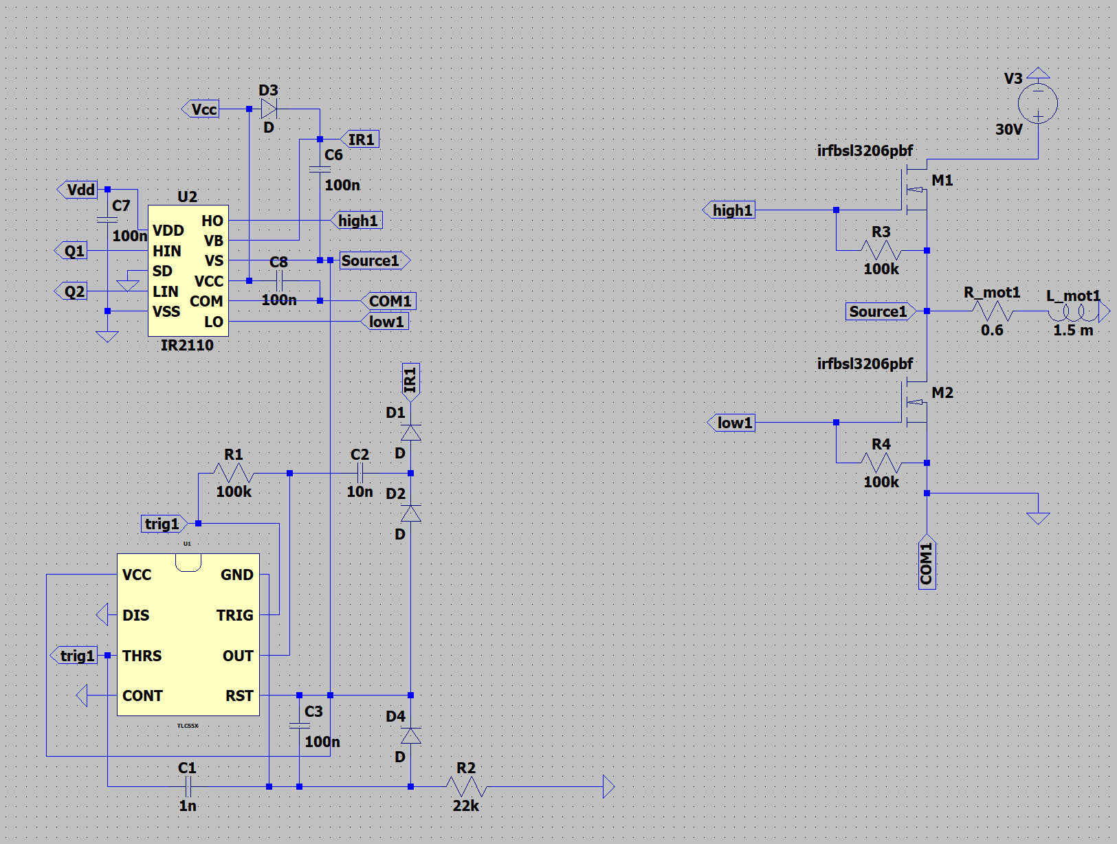
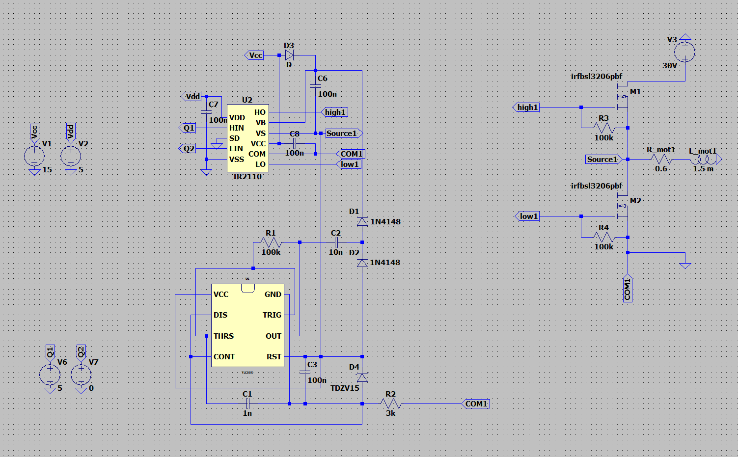
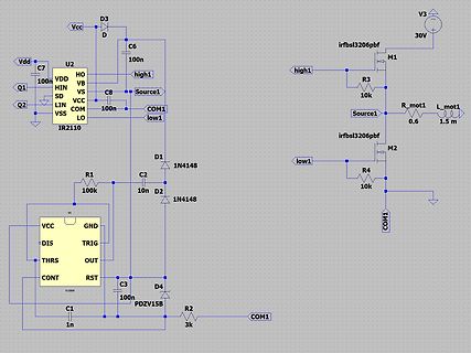
Schaltplan einer Treiberschaltung mit MOSFETs
D3, Vcc, C6, 100n, IR1, high1, U2, Vdd, C7, 100n, Q1, HIN, VB, VS, SD, VCC, COM, LO, LIN, VSS, IR2110, Source1, M1, irfbsl3206pbf, R3, 100k, R_mot1, L_mot1, 0.6, 1.5m, V3, 30V, low1, M2, R4, 100k, COM1, irfbsl3206pbf, low1, IR1, D1, C2, 10n, D2, D, trig1, R1, 100k, U1, GND, VCC, DIS, TRIG, THRS, OUT, CONT, RST, TLC555, C3, 100n, D4, D, R2, 22k, C1, 1n
in „H-Brücke mit 100% Duty-Cycle“ · Analoge Elektronik und Schaltungstechnik · · Schaltpläne
-
PDF
EGS002_manual_en.pdf
driver board specific for single phase sinusoid inverter. It uses ASIC EG8010 as control chip and IR2110S as driver chip. The driver board integrates functions of voltage, current and temperature protection, LED warning indication and fan control.Jumper configures 50/60Hz AC output, soft start mode
in „EGS002 welches Display ist geeignet ?“ · Mikrocontroller und Digitale Elektronik ·
-
PDF
EGS002_manual.pdf
driver board specific for single phase sinusoid inverter. It uses ASIC EG8010 as control chip and IR2110S as driver chip. The driver board integrates functions of voltage, current and temperature protection, LED warning indication and fan control.Jumper configures 50/60Hz AC output, soft start mode
in „Inverter DC/AC mit EGS002 China DEV-Board“ · Analoge Elektronik und Schaltungstechnik ·
-
 Bild
Bild
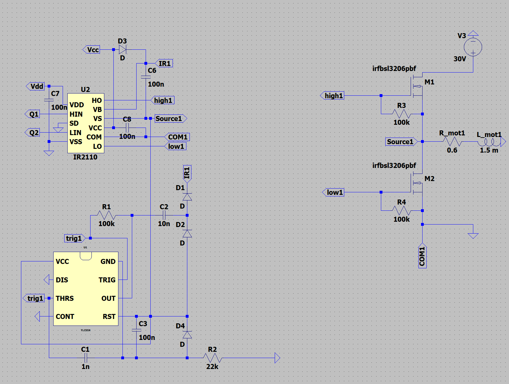
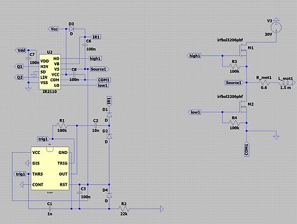
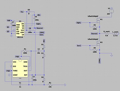
Schaltplan einer Treiberschaltung mit MOSFETs
D3, Vcc, C6, 100n, IR1, high1, U2, Vdd, Q1, HIN, VB, VS, C8, Source1, VCC, COM1, low1, IR2110, Q2, LIN, COM, LO, VSS, R3, 100k, irfbsl3206pbf, M1, R_mot1, L_mot1, 0.6, 1.5m, V3, 30V, irfbsl3206pbf, M2, low1, R4, 100k, COM1
in „H-Brücke mit 100% Duty-Cycle“ · Analoge Elektronik und Schaltungstechnik · · Schaltpläne
-
 Bild
Bild
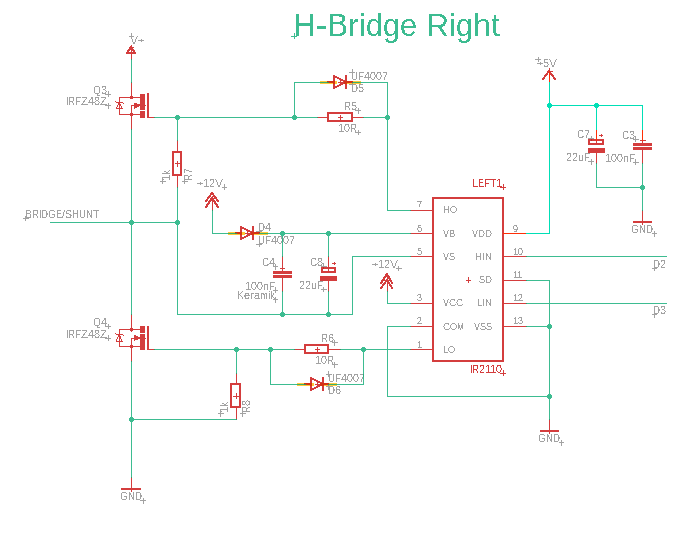
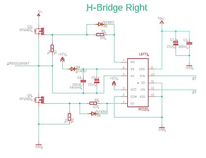
Schaltplan eines H-Brücken-Treiber-Moduls
22uF +12V+ BRIDGE/SHUNT Q4 IRFZ48Z R7 1k R6 10R D6 UF4007 3 + SD 12 2 VCC LIN 13 P2 P3 1 LO 2 COM VSS IR2110 GND
in „Hilfe bei H-Brücke und OPVs fürs Studium“ · Analoge Elektronik und Schaltungstechnik · · Schaltpläne
-
 Bild
Bild
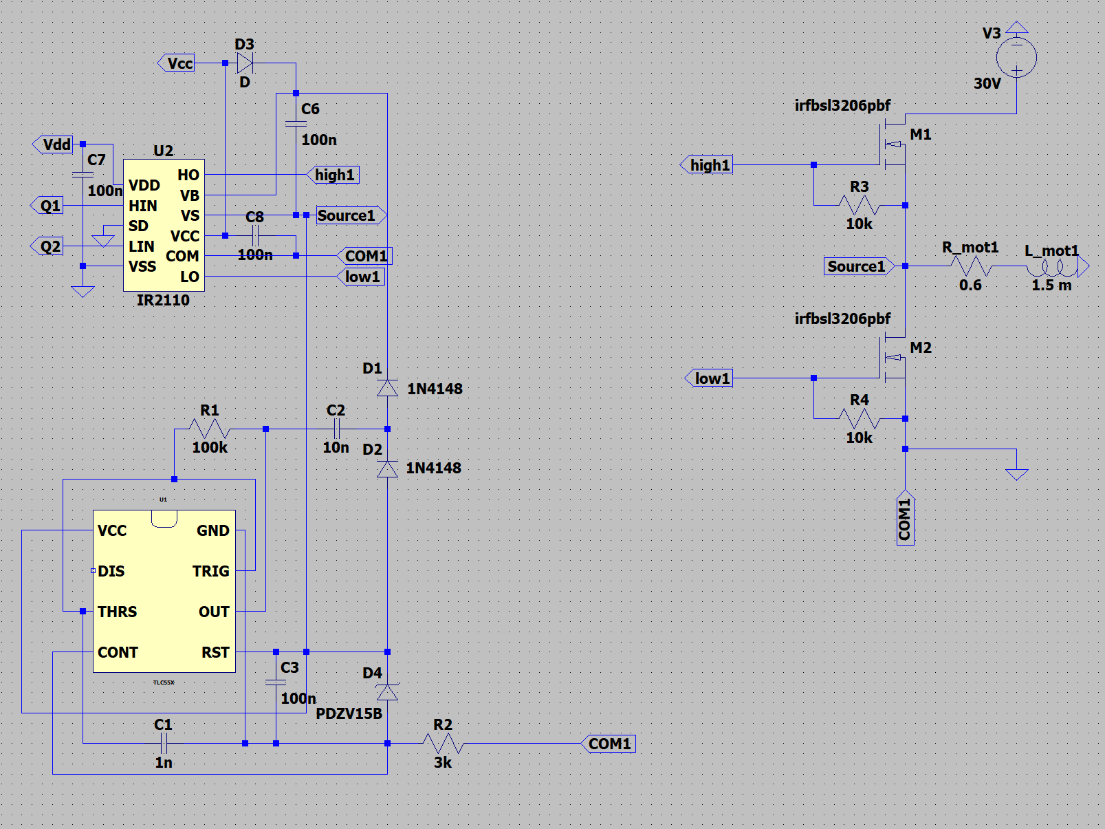
Schaltplan einer Gate-Treiber-Schaltung mit MOSFETs
Vcc D3 V3 30V U2 HO high1 M1 Vdd C7 100n VB IR2110 R3 10k HIN SD VS Source1 C8 100n LIN COM R_mot1 0.6 L_mot1 1.5m COM1 low1 irfbsl3206pbf M2 R4 10k D1 1N4148 low1 D2 1N4148 COM1 R1 100k C2 10n U1 VCC GND DIS TRIG THRS OUT CONT RST C1 1n C3 100n
in „H-Brücke mit 100% Duty-Cycle“ · Analoge Elektronik und Schaltungstechnik · · Schaltpläne
-
 Bild
Bild
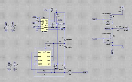
Schaltplan einer MOSFET-Treiberbeschaltung
Vcc V1 V2 D3 C6 U2 high1 IR2110 VD D C7 100k Q1 VB VS VCC 100n COM1 low1 M1 irfbsl3206pbf 30V R3 100k Source1 R_mot1 L_mot1 0.6 1.5m SD LIN COM VSS LO Q2 M2 irfbsl3206pbf low1 R4 100k D1 1N4148 C2 10n D2 1N4148 COM1 VCC GND DIS
in „H-Brücke mit 100% Duty-Cycle“ · Analoge Elektronik und Schaltungstechnik · · Schaltpläne
-
PDF
SNT.pdf
B +C6 X1-1 AC2 AC1 - 470u X1-2 +UB +VREF D 4,7k G A R2 +15V +15V C7 Q4 k IC1 IRF840 1 5 2,2u 1 12 IR2110 P7 R8 1 7 1 +I1 VCC HO R 4 2 14 100n 22 AGND -I1 VREF P9 P6 C12 k +VREF 16 13 C2 VDD VB +C4 , R +I2 OUTC 470p 4 15 8 D 100n P10 P5 4,7u 0 T C3 + -I2 C1 N HIN VS 4 C R6 G +15V 4 F 0 X2-2 3 COMP E1
in „Schaltnetzteil eigenbau.“ · Analoge Elektronik und Schaltungstechnik ·
-
PDF
hp-6236B.pdf
normal time-constant 2-amp fuse (HP Part No. The maximum rated output current is 2.5A and the current 2110-0002). For Options 220 or 240, use a normal time- limit is factory-adjusted to operate at 2.75A ±5% when constant 1-amp fuse (HP Part No. 2110-0001). the output is 6 volts. At lower output voltages,
in „Problem mit Simulation von HP/Agilent Tracking LNG“ · Mikrocontroller und Digitale Elektronik ·
-
PDF
fetdrvr-t.pdf
used, for example, 500V for the International Rec- and switch the MOSFET gate accordingly [1] . tifier IR2110 half bridge driver, and 80V for the Harris HIP4080/1 full bridge driver. The HIP4080 has an high speed input comparator and is easily configured as a 2.2 Adding an isolated power supply hysteretic
in „Ansteuerung H-Vollbrücke“ · Analoge Elektronik und Schaltungstechnik ·
-
PDF
vestel_17mb70_sm.pdf
............................................................................................ 58 D. IR Problem ............................................................................................................................59 E. Keypad Touchpad Problems.....................................
in „LED TV Medion MD 30630 defekt, nicht einmal standby Lampe“ · Analoge Elektronik und Schaltungstechnik ·
-
PDF
UM08001_JLinkARM.pdf
operations of the circuitry. TAP controller state diagram Reset tms=1 tms=0 Idle tms=1 DR-Scan tms=1 IR-Scan tms=1 tms=0 tms=0 tms=0 tms=1 Capture-DR tms=1 Capture-IR tms=0 tms=0 Shift-DR Shift-IR tms=1 tms=0 tms=1 tms=0 Exit1-DR tms=1 Exit1-IR tms=1 tms=0 tms=0 Pause-DR Pause-IR tms=1 tms=0 tms=1 tms=
in „[V] J-Link JTAG Adapter USB für ARM abzugeben“ · Markt ·
-
PDF
C65_Diagram_Set.pdf
USART1_CTS C20 - G RF_AFC C1001 A9 AFC USART1_RTS C17 - RF_SIN26M R1006 30K F26M USART1_TXD SW_TP1006 IR_AC_TX D 18P 15P AE15 C21 N AD15 F32K USART1_RXD C19 IR_AC_RX G 2 OSC32K E C1002 H SW_TP1035 AE16 E D K PM_RTC_INT - RTC_OUT USART0_CTS2 Z1000 N 8 -W_TP1015AD14 AD19 t G 7M_RESET_N AE17 RESET USART0_CTS1
in „Reengineering: Siemens S65 Display“ · Mikrocontroller und Digitale Elektronik ·
-
PDF
5959-5329_SCH_E3630A.pdf
Fuse Agilent Part No. indicators for +6V output, +20V output, and -20V output, a 100/115 Vac 1.6 A 2110-0918 voltmeter and an ammeter, and three push-button meter 230 Vac 1.0 A 2110-0599 switches. The push buttons select one of the supply's three outputs for display. The voltmeter and ammeter always moni
in „Labornetzgerät als Projekt“ · Analoge Elektronik und Schaltungstechnik ·
-
PDF
5959-5329_SCH_E3630A.pdf
Fuse Agilent Part No. indicators for +6V output, +20V output, and -20V output, a 100/115 Vac 1.6 A 2110-0918 voltmeter and an ammeter, and three push-button meter 230 Vac 1.0 A 2110-0599 switches. The push buttons select one of the supply's three outputs for display. The voltmeter and ammeter always moni
in „Problem mit Simulation von HP/Agilent Tracking LNG“ · Mikrocontroller und Digitale Elektronik ·
-
PDF
MT6252.pdf
15 14 13 12 1IRQ1D10 9 8 7 6 R e l e4 3IRQ1C2 1 0 Reset 0x1d n t i a l 0x1c n f id e 0xBit1_0310 30 IR29Sele28ioC 27oegi26er 25 24 23 22 21 20 19 18 IRQ17EL816 NType d i a T e IR/W3 IR/W2 ResMt e 0x23 X 0x22 Namet 15 14 13 12 1IRQ2110 9 8 7 _ W 6 C 5 4 3IRQ202 1 0 Reset 0x21 e n o n 0x20 0x8101_0024 IRQ
in „Amparos GPS Tacker - Pollin Schnäppchen“ · Mikrocontroller und Digitale Elektronik ·
-
PDF
33120-90017.pdf
500 mA part (part number 2110-0716). The fuse is located near the output connector (J801) on the main PC board. You will need to disassemble the function generator to replace this fuse (use a TORX T-15 driver to remove the screws
in „Projekt: DDS basierter Funktionsgenerator mit AD5930“ · Mikrocontroller und Digitale Elektronik ·
-
PDF
Hewlett_Packard_Operating_and_Service_Manuals_for_HP361XA_30W_Bench_Series_DC_Power_Supplies.pdf
fT'li, KB°D *;^;;i T - x (jifjife) ^-^^/TLs-ro c0?aD°pli, ( ^ x iot«?§r•To ®S0/S;l^1±^iR/Mli;Si6-5/;*ir, NVARNINCI IEL < ft*7/i A'->/;JS-&i;A:S-±®1« «SS0-> + - i /ir + tf:^. v MiSm6^(C}|^JlbL''j:itn(i' ^^?i^^c-r^S6tt0*.'i>^ii'fii 'i•o*•t*•^<, m f5 3^$?Ei(?.3 >-b> h0!E»,}^ttb ( ^ ^ y ^ - ^ ^ K) ir LoA^OtJ
in „Gebrauchtes Labornetzteil HP Agilent“ · Mechanik, Gehäuse, Werkzeug ·
-
PDF
ILI9325.pdf
. The interface mode is selected by setting the IM[3:0] pins. ILI9325 has a 16-bit index register (IR), an 18-bit write-data register (WDR), and an 18-bit read-data register (RDR). The IR is the register to store index information from control registers and the internal GRAM. The WDR is the register
in „Programmierung von ILI9325 TFT Display“ · Mikrocontroller und Digitale Elektronik ·
-
PDF
ILI9325DS_V0.35.pdf
. The interface mode is selected by setting the IM[3:0] pins. ILI9325 has a 16-bit index register (IR), an 18-bit write-data register (WDR), and an 18-bit read-data register (RDR). The IR is the register to store index information from control registers and the internal GRAM. The WDR is the register
in „[V]erkaufe TFT 2.8" und TFT 2.4" mit adapter PCB“ · Markt ·
-
PDF
ILI9325DS_V0.28.pdf
. The interface mode is selected by setting the IM[3:0] pins. ILI9325 has a 16-bit index register (IR), an 18-bit write-data register (WDR), and an 18-bit read-data register (RDR). The IR is the register to store index information from control registers and the internal GRAM. The WDR is the register
in „Chinesisches TFT LCD zum Schnäppchenpreis“ · Mikrocontroller und Digitale Elektronik ·
-
PDF
Datasheet_ILI9225DS_V022.pdf
. The interface mode is selected by setting the IM[3:0] pins. ILI9225 has a 16-bit index register (IR), an 18-bit write-data register (WDR), and an 18-bit read-data register (RDR). The IR is the register to store index information from control registers and the internal GRAM. The WDR is the register
in „STM32F103 TFT SPI ILI9225“ · Mikrocontroller und Digitale Elektronik ·
-
PDF
ili9328.pdf
. The interface mode is selected by setting the IM[3:0] pins. ILI9328 has a 16-bit index register (IR), an 18-bit write-data register (WDR), and an 18-bit read-data register (RDR). The IR is the register to store index information from control registers and the internal GRAM. The WDR is the register
in „VW-Werbebeilage mit Display (vidipri)“ · Mikrocontroller und Digitale Elektronik ·
-
PDF
ILI9328DS_V0.1.pdf
. The interface mode is selected by setting the IM[3:0] pins. ILI9328 has a 16-bit index register (IR), an 18-bit write-data register (WDR), and an 18-bit read-data register (RDR). The IR is the register to store index information from control registers and the internal GRAM. The WDR is the register
in „[V]erkaufe TFT 2.8" und TFT 2.4" mit adapter PCB“ · Markt ·
-
PDF
kicad_8450_dcm_liste_neu_v3.pdf
Protected Class D Audio Amplifier Half-Bridge Gate Driver, Output Current 1.0/1.2A, +/-100V, SOIC-16 IR2104 High and Low Side Gate Driver, Output Current 130/270mA, PDIP-8 , SOIC-8 IR2106 High and Low Side Driver, 600V operation, Output Current 120/200mA, PDIP-8 , SOIC-8 IR2110 High and Low Side Gate Driver
in „KiCAD Eeschema, Bibliotheksdokumentation *.dcm als PDF-Datei“ · Platinen ·
-
PDF
HD66766-10.pdf
The IM2-0 pins select the interface mode. The HD66766 has three 16-bit registers: an index register (IR), a write data register (WDR), and a read data register (RDR). The IR stores index information from the control registers and the GRAM. The WDR temporarily stores data to be written into control registers
in „The Siemens S65 132x176, 65536 color display with AVR“ · Projekte & Code ·