-
PDF
5kV_200ns_Pulsed_Power_Switch_based_on_SiC-Cascode.pdf
SiC JFET devices with 1 avalanche a blocking voltage of 1.5kV per JFET are available. Alternatively, the operating voltage could be increased by connecting N JFETs Low-Voltage Si MOSFET and a low voltage MOSFET
in „Pulsgenerator zur Plasmaerzeugung“ · Analoge Elektronik und Schaltungstechnik ·
-
PDF
biela_SicSwitch_P_5kV_200ns.pdf
At the moment SiC JFET devices with a blocking voltage of 1.5kV per JFET are available. Alternatively, the operating voltage could be increased by connecting N JFETs Low-Voltage Si MOSFE0V and a low voltage MOSFET in series
in „1500V 8A mit MOSFET schalten“ · Analoge Elektronik und Schaltungstechnik ·
-
PDF
Amplifiers_and_Comparators_-_Motorola.pdf
25 4.0 13 〉 5.0 〉 18 Low Noise, JFET Input D/751 TL081AC 200 pA 6.0 10 100 pA 50 4.0 13 〉 5.0 〉 18 JFET Input P/626 TL081C 400 pA 15 10 200 pA 25 4.0 13 〉 5.0 〉 18 JFET Input D/751 Automotive Temperature Range (–40⋅C to +85⋅C) MC33071
in „AVR: Wechseln des Kanals mit automatischem Trigger“ · Mikrocontroller und Digitale Elektronik ·
-
PDF
AN101_An_Introduction_to_FETs_70594__VIS.pdf
Implicit in this de- satility of the FET family: scription is the fundamental difference between JFET and Amplifiers Switches bipolar devices: when the JFET junction is reverse-biased the gate current is practically zero, whereas the base cur- ▯ Small Signal ▯ Chopper-Type rent of the bipolar transistor
in „mit 2,7V schalten“ · Mikrocontroller und Digitale Elektronik ·
-
PDF
umschaltung_fet.pdf
1 2 3 4 433 A A P3Q1031 P1Q101 P1Q2012 P3Q203 0 0 0 0 P P JFET-N JFET-N 3 4 01 Q3 01 P P JFET-N Q4 P0Q302 JFET-N 3 2 P2Q402 3 3 4 P P B B P GND GND IC N P0Q5035 P1Q501 P0Q6016 P3Q603 0 0 2 2 P P JFET-N JFET-N C 0 0 C 01 01 P Q7 P JFET-N Q8 P2Q702 P0Q802 JFET-N
in „Eingangskreis Umschaltung ohne Relais?“ · HF, Funk und Felder ·
-
PDF
0401Koster58.pdf
or A unique, low- less, selection of an appropriate circuit becomes more and more restricted. The JFET elements voltage, source- This discussion revolves around a lesser-known oscillator circuit that uses two junction field-effect transistors (JFET) as active devices. Due to the coupled J-FET VCO high
-
PDF
Koster58_VFO.pdf
or A unique, low- less, selection of an appropriate circuit becomes more and more restricted. The JFET elements voltage, source- This discussion revolves around a lesser-known oscillator circuit that uses two junction field-effect transistors (JFET) as active devices. Due to the coupled J-FET VCO high
in „Clapp Oszillator mit oder ohne Bandpassfilter“ · HF, Funk und Felder ·
-
PDF
0401Koster58.pdf
or A unique, low- less, selection of an appropriate circuit becomes more and more restricted. The JFET elements voltage, source- This discussion revolves around a lesser-known oscillator circuit that uses two junction field-effect transistors (JFET) as active devices. Due to the coupled J-FET VCO high
in „LC Oszillator beliebige LC Verhältnisse“ · HF, Funk und Felder ·
-
PDF
PSpice_LibraryguideOrCAD.pdf
TransistoJ310 J310 JFET.OLB Junction Field-Effect TransistoJ401 J401 JFET.OLB Junction Field-Effect TransistoJ402 J402 JFET.OLB Junction Field-Effect TransistoJ403 J403 JFET.OLB Junction Field-Effect TransistoJ404 J404 JFET.OLB
in „pSpice - Bauteil hinzufügen.“ · Analoge Elektronik und Schaltungstechnik ·
-
PDF
TL061CP.pdf
+ TL061 . . . U PACKAGE D Output Short-Circuit Protection (TOP VIEW) D High Input Impedance . . . JFET-Input Stage NC •1 NC D Internal Frequency Compensation 10 OFFSET N1 2 9 NC D Latch-Up-Free Operation IN– 3 8 VCC+ D High Slew Rate . . . 3.5 V/µs Typ 4 IN+ 7 OUT VCC– 5 6 OFFSET N2 description The JFET-input
in „Messspannung von Shunt verstärken, kfz“ · Analoge Elektronik und Schaltungstechnik ·
-
PDF
DS_UJ3N120070K3S-1530204.pdf
70mW - 1200V SiC Normally-On JFET | UJ3N120070K3S Datasheet Description CASE CASE United Silicon Carbide, Inc offers the high-performance G3 SiC normally- D (2) on JFET transistors. This series exhibits ultra-low on resistance () DS
in „SiC Kaskoden Body Diode“ · Analoge Elektronik und Schaltungstechnik ·
-
Datei
main.c
(mosfet); //"-MOS" } else { if((PartMode==PART_MODE_N_JFET) || (PartMode==PART_MODE_P_JFET)) { lcd_eep_string(jfet); //"-JFET" } else { lcd_eep_string(emode); //"-E" lcd_eep_string(mosfet); //"-MOS" } } #ifdef UseM8 //Gatekapazität if(PartMode < 3) { //Anreicherungs-MOSFET
-
PDF
tle2082.pdf
TLE208x, TLE208xA, TLE208xY EXCALIBUR HIGH-SPEED JFET-INPUT OPERATIONAL AMPLIFIERS SLOS182B – FEBRUARY 1997 – REVISED JUNE 2001 D Direct Upgrades to TL05x, TL07x, and D On-Chip Offset Voltage Trimming for TL08x BiFET Operational Amplifiers Improved DC
in „Bauteil gesucht: unbekannter TI-Baustein“ · Mikrocontroller und Digitale Elektronik ·
-
PDF
LSM_LSK389_SOIC.pdf
LSK389 ULTRA LOW NOISE MONOLITHIC DUAL N-CHANNEL JFET Linear Systems replaces discontinued Toshiba 2SK389 with LSK389 The 2SK389 / LSK389 is a monolithic matched dual JFET on a single chip Why use On-Chip Dual JFET instead of 2 single JFETS? Save Cost 2SK389 / LSK389 removes significant cost for test screening time needed to match I DSSon 2 individual JFETS and offers ZERO yield loss. Improve Performance 2SK389 / LSK389 On-Chip I DSSmatching gives closest possible synchronous electrical performance and also offers better matched performance when the chip
in „Suche Transistor "K389" für Technics SU-VX 800“ · Analoge Elektronik und Schaltungstechnik ·
-
Bild
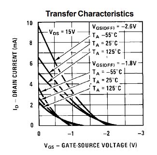
Diagramm der Transferkennlinie eines MOSFETs
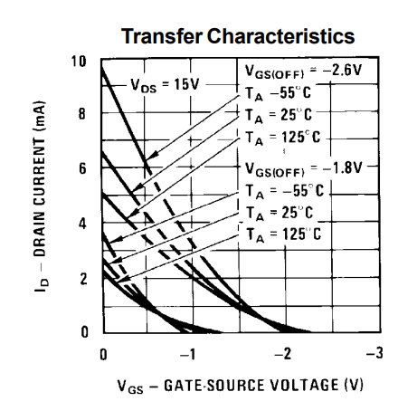
Transfer Characteristics 10 8 6 4 2 0 0 -1 -2 -3 ID DRAIN CURRENT (mA) VGS - GATE-SOURCE VOLTAGE (V) VDS = 15V VGS(OFF) = -2.6V TA = -55°C TA = 25°C TA = 125°C VGS(OFF) = -1.8V TA = -55°C TA = 25°C TA = 125°C
in „Wie wird eine hochgenaue (absolute) Spannungsreferenz hergestellt?“ · Analoge Elektronik und Schaltungstechnik · · Diagramme
-
Datei
JFet_models.txt
.MODEL BF245A NJF(VTO=-1.7372E+000 BETA=1.16621E-003 LAMBDA=1.77211E-002 RD=9.01678E+000 RS=9.01678E+000 IS=2.91797E-016 CGS=2.20000E-012 CGD=2.20000E-012 PB=7.80988E-001 FC=5.00000E-001) .MODEL BF245B NJF(VTO=-2.3085E+000 BETA=1.09045E-003 LAMBDA=2.31754E-002 RD=7.77648E+000 RS=7.77648E+000 IS=2.59121E-016 CGS=2.00000E-012 CGD=2.20000E-012 PB=9.91494E-001 FC=5.00000E-001) .model BF245C NJF(VTO=-5.0014E+000 BETA=5.43157E-004 LAMBDA=2.71505E-002 RD=1.20869E+001 RS=1.20869E+001 IS=3.64346E-016 CGS=2.00000E-012 CGD=2.00000E-012 PB=1.24659E+000 FC=5.00000E-001) .model BF256B NJF(VTO=-2.3085E+000 BETA=
in „fest abgestimmte 80m-Loopantenne“ · HF, Funk und Felder ·
-
Bild
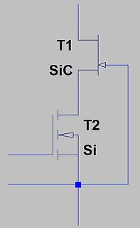
Schaltplan mit SiC und Si Transistoren
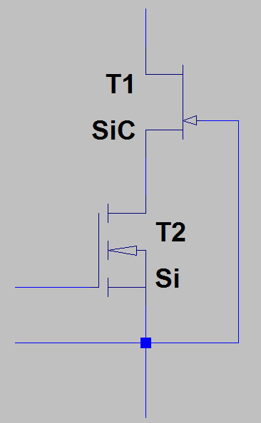
T1 SiC T2 Si
in „Unerwünschter Peak beim Ausschalten eines Kleinsignal-MOSFET“ · Analoge Elektronik und Schaltungstechnik · · Schaltpläne
-
Bild
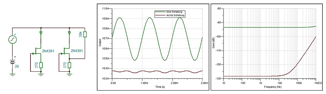
Schaltplan und Messkurven einer Schaltung
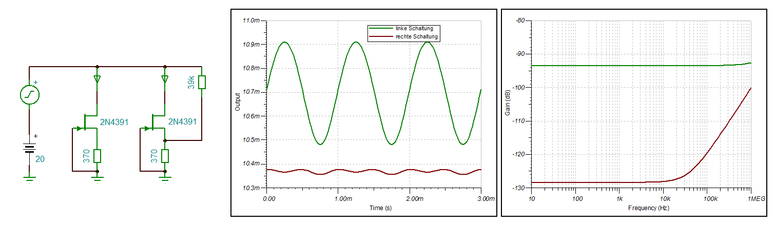
2N4391 39k 20 370 370 linke Schaltung rechte Schaltung Output 11.0m 10.9m 10.8m 10.7m 10.6m 10.5m 10.4m 10.3m Time (s) 0.00 1.00m 2.00m 3.00m -80 -90 -100 -110 -120 -130 Gain (dB) 100 1k 10k 100k 1MEG
in „Topologie Konstantstromsenke“ · Analoge Elektronik und Schaltungstechnik · · Screenshots
-
PDF
tidu765.pdf
contact with it must have extremely high input impedance. Most electret microphones have an internal JFET which buffers the microphone capacitor. The voltage signal produced by sound modulates the gate voltage of the JFET, labeled V inGFigure 2 causing a change in the current flowing between the drain and source of the JFET (I MIC). An extremely high resistance, R ,Gmay be included to bias the gate of the JFET. Microphone Capacitor with Electret MIC V G JFET Sound Wave R G Figure 2: A simplified circuit schematic of an
in „Hilfe! Mikrofone im Tetraeder so so ganz billige für nen Roboter!“ · Analoge Elektronik und Schaltungstechnik ·
-
Bild
Transistor-Kurven-Tracer mit Display und Kennlinien
Bat 5.5 Curve Tracer SETUP PNP NPN MOSFET JFET PNP Gain=123 n-JFET Voff=3.8 n-MOSFET Thresh=1.8 Curves for PNP Gain=150 Curves for MOSFET Curves for JFET Main Menu Bat 6.2 PNP NPN MOSFET JFET
in „[S] Kennlinienschreiber für Oszilloskop“ · Markt · · Fotos
-
PDF
Vishay-Silcnx_FET_VoltCntrlRES_AN105.pdf
operating characteristics of an n- three-terminal variable resistor where the resistance val- channel JFET. Most amplification or switching operations ue between two of the terminals is controlled by a voltage of FETs occur in the constant-current (saturated) region, potential applied to the third. shown
in „Spannungsgeregelter Widerstand“ · Analoge Elektronik und Schaltungstechnik ·
-
PDF
ttester.pdf
53pF 43pF 44pF IRFU9024 P-E-MOS,D, 3.5V P-E-MOS,D, 3.6V P-E-MOS,D, 3.5V 937pF 945pF 952pF J310 N-JFET N-JFET N-JFET Idss=24-60mA I=3.1mA Vgs=2.2V I=3.1mA Vgs=2.2V I=3.1mA Vgs=2.2V 2N5459 N-JFET N-JFET N-JFET Idss=4-16mA I=2.1mA Vgs=1.5V I=2.1mA Vgs=1.5V I=2.1mA Vgs=1.5V BF256C N-JFET N-JFET N-JFET Idss=11-18mA I=3.4mA Vgs=2.4V I=3.4mA Vgs=2.4V I=3.4mA Vgs=2.4V BF245A N-JFET N-JFET N-JFET Idss=2-6mA I=1.1mA Vgs=.75V I=1.1mA Vgs=0.75V I=1.1mA Vgs=0.75V BF245B N-JFET N-JFET N-JFET Idss=6-15mA I=2.5mA Vgs=1.7V I=2.5mA Vgs=1.7V I=2.5mA Vgs=1.7V BF245C N-JFET N-JFET N-JFET Idss
in „Sammelbestellung Transistortester III - schnelle Runde“ · Markt ·
-
PDF
ttester_ger109k.pdf
53pF 43pF 44pF IRFU9024 P-E-MOS,D, 3.5V P-E-MOS,D, 3.6V P-E-MOS,D, 3.5V 937pF 945pF 952pF J310 N-JFET N-JFET N-JFET Idss=24-60mA I=3.1mA Vgs=2.2V I=3.1mA Vgs=2.2V I=3.1mA Vgs=2.2V 2N5459 N-JFET N-JFET N-JFET Idss=4-16mA I=2.1mA Vgs=1.5V I=2.1mA Vgs=1.5V I=2.1mA Vgs=1.5V BF256C N-JFET N-JFET N-JFET Idss=11-18mA I=3.4mA Vgs=2.4V I=3.4mA Vgs=2.4V I=3.4mA Vgs=2.4V BF245A N-JFET N-JFET N-JFET Idss=2-6mA I=1.1mA Vgs=.75V I=1.1mA Vgs=0.75V I=1.1mA Vgs=0.75V BF245B N-JFET N-JFET N-JFET Idss=6-15mA I=2.5mA Vgs=1.7V I=2.5mA Vgs=1.7V I=2.5mA Vgs=1.7V BF245C N-JFET N-JFET N-JFET Idss
in „Sammelbestellung Transistortester III - schnelle Runde“ · Markt ·
-
PDF
SMD_Catalog.pdf
MMBF4093 Nat F - n-ch jfet sw/chopper 61M MMBF4859 Nat F - n-ch jfet sw/chopper 61N MMBF5514 Nat F - p-ch jfet sw/chopper 61P MMBF5115 Nat F - p-ch jfet sw/chopper 61Q MMBF5516 Nat F - p-ch jfet sw/chopper 61S MMBF5458 Nat F
in „Hilfe bei Bauteilsuche für Mainboard“ · PC Hard- und Software ·
-
PDF
05_03-12-LTC1968-Pei.pdf
oftheJFETtomodulatetheamplitude positivefeedbackRCnetworkgenerate bias. Changing the bias of the JFET accordingly. As shown, the output the oscillations. The amplitude, and adjuststhegainoftheoscillator,and amplitudeof thesinewaveis amplitude stability, of the sine wave thus the amplitude of the resulting
in „Sinus-Oszillator“ · Analoge Elektronik und Schaltungstechnik ·
-
PDF
AB-064.pdf
orders of magnitude. Step D S OPA FETsaregenerallymuchbetterinthisrespect,andSiliconix’s 4 6 2N4117A JFET proves the best. r Figure 2 shows an experimentally derived curve of leakage OVERVOLTAGE PROTECTION results when you incorporate a diode- e connected JFET in the measuring circuit. If the dielectric
in „Ersatz für BAV45“ · Analoge Elektronik und Schaltungstechnik ·
-
PDF
JFET-based_300-mV_supply.pdf
EDITED BY BRAD THOMPSON AND FRAN GRANVILLE d e s i g n i d e a s READERS SOLVE DESIGN PROBLEMS JFET-baseddc/dcconverter DIs Inside operatesfrom300-mVsupply 94 Configurable logic gates’ Jim Williams, Linear Technology Corp, Milpitas, CA versatile monostables ▯ characteristics to build a dc/dc many
in „Boost Converter / Step Up mit 150mV eingang“ · Analoge Elektronik und Schaltungstechnik ·
-
Bild
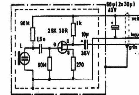
Schaltplan einer JFET-Schaltung
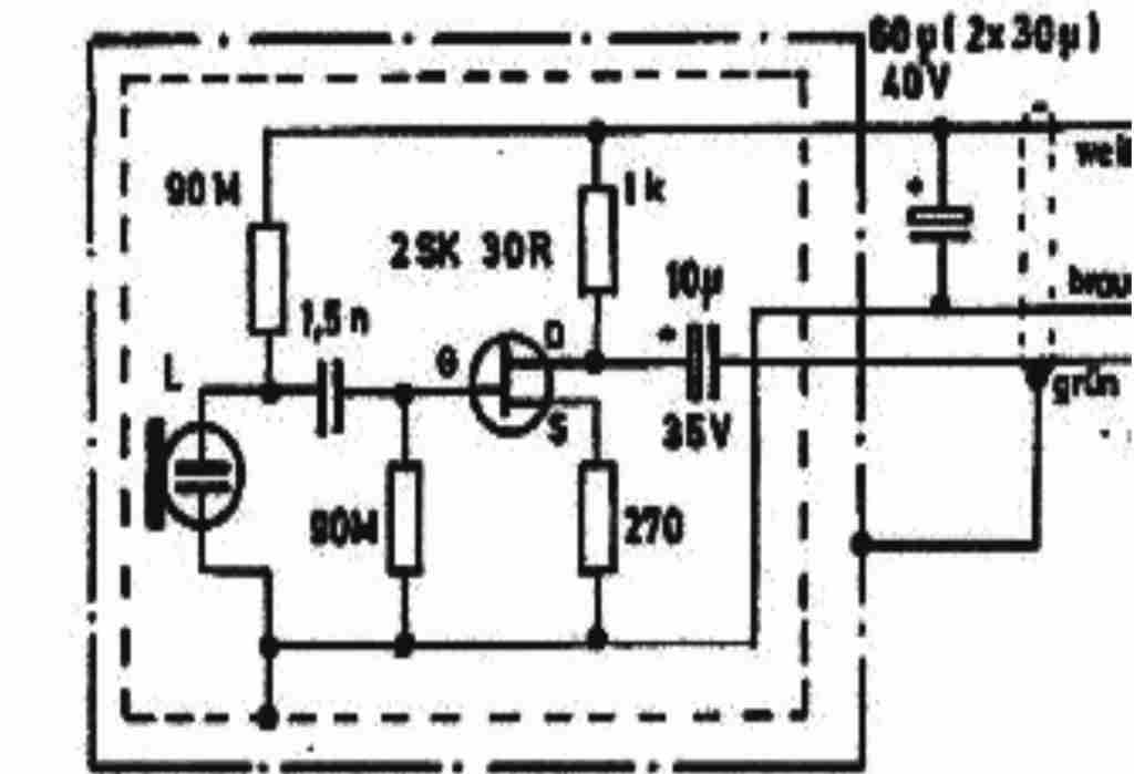
60µ (2x30µ) 40V well broun grn 90M 2SK 30R 1k 10µ 35V 1,5n G D S 90M 270 L
in „Micro mit Phantomspeisung - Fehlerdiagnose“ · Analoge Elektronik und Schaltungstechnik · · Schaltpläne
-
Bild
Schaltplan eines Kristalloszillators mit JFET
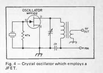
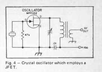
OSCILLATOR MPF102 G D S 47k .01 RF OUT + VDD Fig. 4 - Crystal oscillator which employs a JFET.
in „Verständnisfrage: Quarzoszillator mit JFET“ · HF, Funk und Felder · · Schaltpläne
-
Bild
Schaltplan einer JFET-Verstärkerschaltung
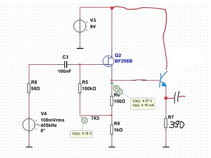
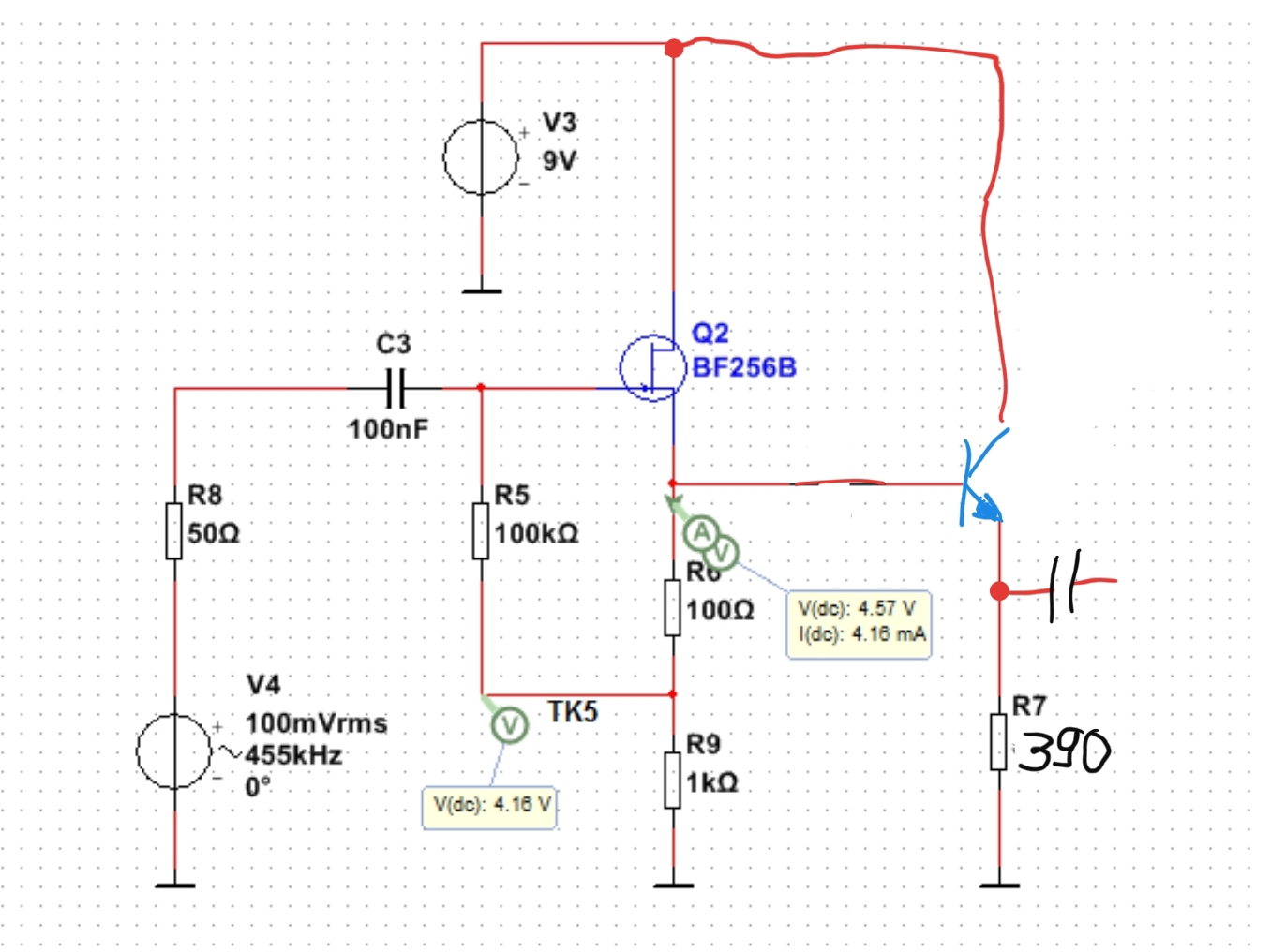
V3 9V Q2 BF256B C3 100nF R8 50Ω R5 100kΩ R6 100Ω V(dc): 4.16 V TK5 R9 1kΩ V(dc): 4.57 V I(dc): 4.16 mA R7 390 V4 100mVrms 455kHz 0°
in „Hilfe bei JFET Impedanzwandler“ · HF, Funk und Felder · · Schaltpläne
-
Bild
Schaltplan eines JFET-Verstärkers
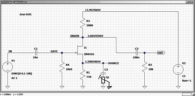
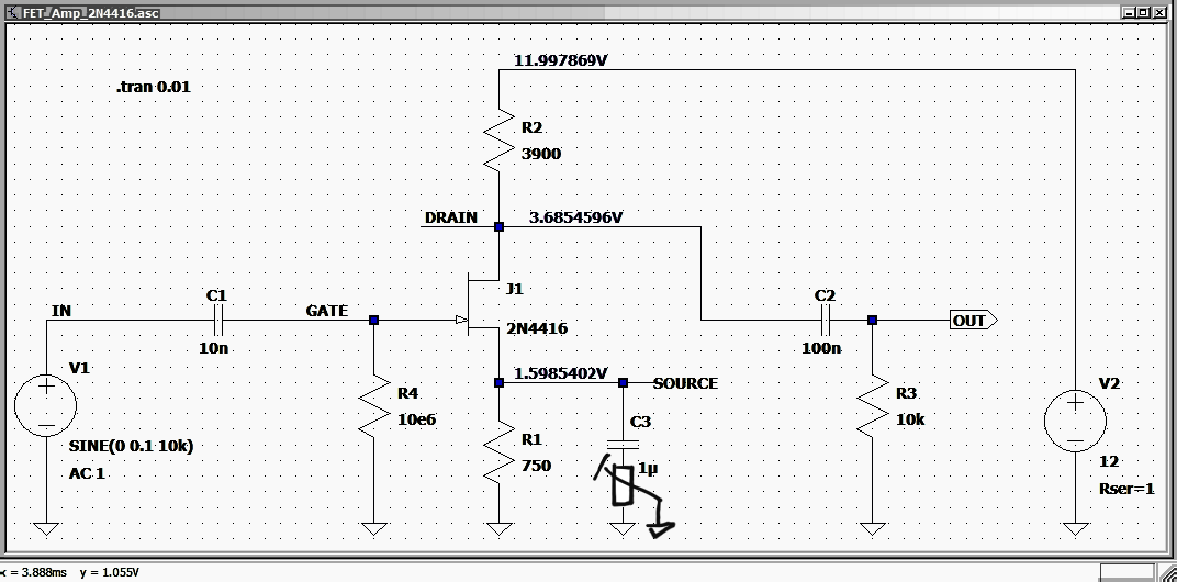
FET:Amp_2N4416.asc .tran 0.01 R2 3900 11.997869V DRAIN 3.6854596V J1 2N4416 C2 100n OUT V2 12 Rser=1 SOURCE 1.5985402V R3 10k C3 1µ R1 750 R4 10e6 GATE C1 10n IN V1 SINE(0 0.1 10k) AC 1
in „Hilfe bei JFET Impedanzwandler“ · HF, Funk und Felder · · Screenshots
-
Bild
Schaltplan einer JFET-Schaltung
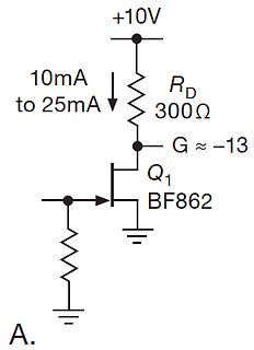
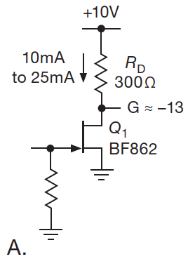
+10V 10mA to 25mA RD 300Ω G ≈ -13 Q1 BF862 A.
in „JFET-Common-Spurce-Verstärker“ · Analoge Elektronik und Schaltungstechnik · · Schaltpläne
-
PDF
Active_antenna_coupler_for_VLF.pdf
cable) The output transformer in fig. 1 is operated in a with some details step-down mode from the jfet drain terminal to pro- vide a higher current driver for the cable at a 150- to for extending 350-ohm impedance level. Fifty-ohm cable is not a perfect match, but at these low frequencies the cable the
-
PDF
LMH6518.pdf
in Figure 6: cator on the screen that alerts the user of the situation so that 30068835 FIGURE 13. JFET LNA Implementation CIRCUIT OPERATION For a flat frequency response, the DC (low frequency) gain This circuit uses an N-Channel JFET (J10) in Source-Follow- needs to be lowered to match the less-than
in „Wittig(welec) DSO W20xxA Hardware“ · Mikrocontroller und Digitale Elektronik ·
-
Bild
Spektrum- und Waterfall-Anzeige eines Spektrumanalysators
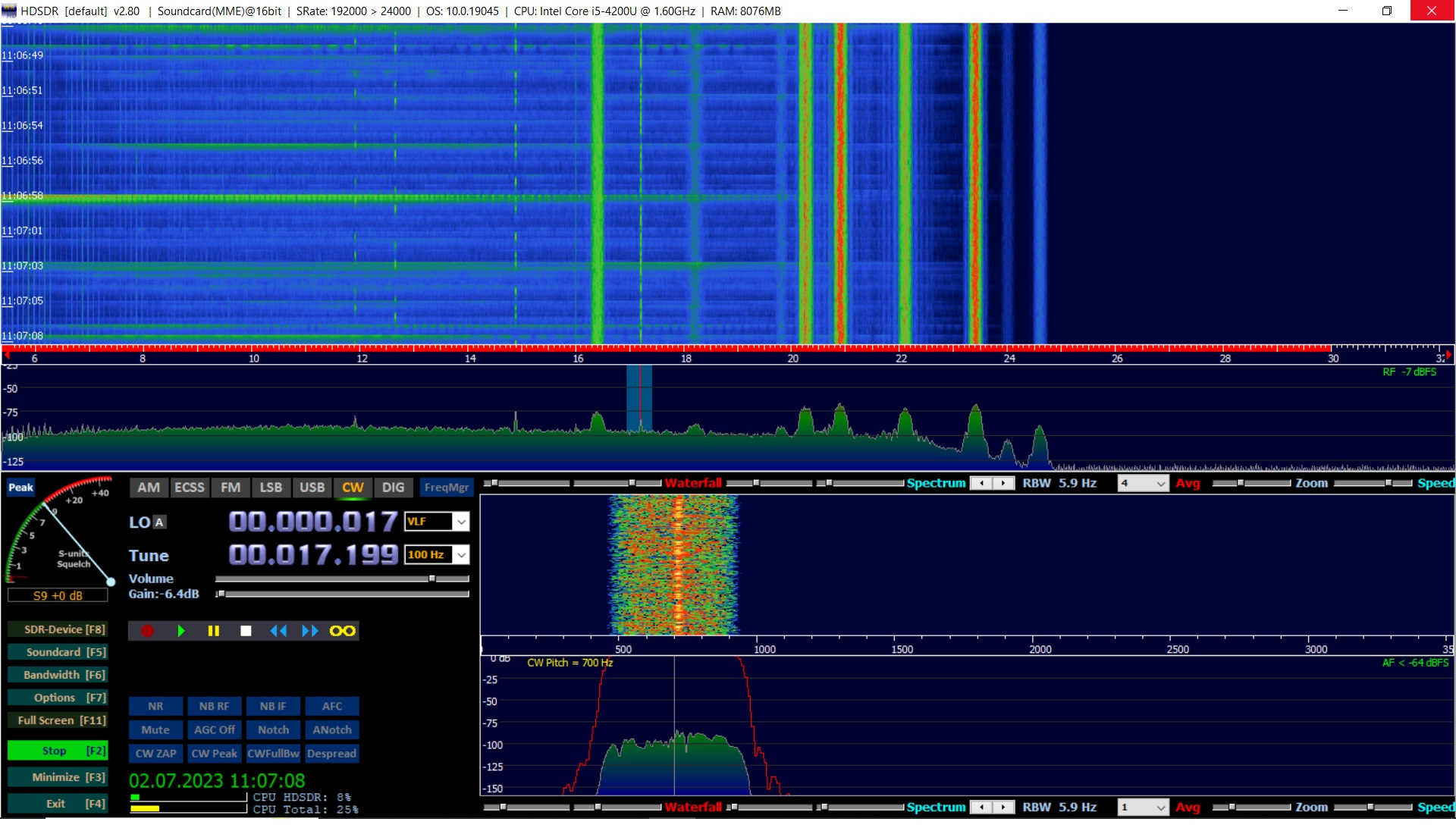
HDSDR [default] V2.80 | Soundcard(MME) | SRate: 192000 | CS: 10.0.19045 | CPU: Intel Core i5-4200U @ 1.60GHz | RAM: 8076MB | Peak +40 | LO A 00.000,017 VLF | Tune 00.017.199 100 Hz | Volume Gain: -6.4dB | Waterfall | Spectrum RBW 5.9 Hz | Avg | Zoom | Speed | 02.07.2023 11:07:08 | CPU HDSR: 8% | CPU Total: 25%
in „SAQ Minimalempfänger“ · HF, Funk und Felder · · Screenshots
-
PDF
Hantek_DSO5062B_250MHz_input_stage_mod.pdf
case I’ll explain why. 1. R01_2 The first part of the input stage – from the BNC connector to the JFET – actually took me the most time to solve. The situation at the beginning was that, even though my test signal would be perfectly fed in at 50 ohms without distortion - when it arrived at the JFET it
-
PDF
esr_bn_17.09.13__original__Kopie.pdf
(10 Punkte) Fig. 2: n-Mosfet als Schalter Fig.3: Ausgangskennlinienfeld n-Mosfet Aufgabe 4: Der n-JFET-Kleinsignalverstärker in Fig. 4 ist für die Verstärkung von Wechselspannungssignalen entworfen. Die Widerstände R und Rdsind ss gewählt, daß sich ein Verstärkungsfaktor von 5 ergibt und sich an R ein
-
PDF
mosfet.pdf
shows the physical origin of the parasitic components in an n-channel power MOSFET. The parasitic JFET appearing between the two body implants restricts current flow when the depletion widths of the two adjacent body diodes extend into the drift region with increasing drain voltage. The parasitic BJT
in „MOSFET - welche Leistung?“ · Analoge Elektronik und Schaltungstechnik ·
-
PDF
mosfet.pdf
shows the physical origin of the parasitic components in an n-channel power MOSFET. The parasitic JFET appearing between the two body implants restricts current flow when the depletion widths of the two adjacent body diodes extend into the drift region with increasing drain voltage. The parasitic BJT
in „NT mit Mosfet“ · Analoge Elektronik und Schaltungstechnik ·
-
PDF
Mosfet-Basics-IR.pdf
shows the physical origin of the parasitic components in an n-channel power MOSFET. The parasitic JFET appearing between the two body implants restricts current flow when the depletion widths of the two adjacent body diodes extend into the drift region with increasing drain voltage. The parasitic BJT
in „MOSFET Sättigung“ · Analoge Elektronik und Schaltungstechnik ·
-
PDF
Hantek_DSO5062B_250MHz_input_stage_mod_r2.pdf
case I’ll explain why. 1. R01_2 The first part of the input stage – from the BNC connector to the JFET – actually took me the most time to solve. The situation at the beginning was that, even though my test signal would be perfectly fed in at 50 ohms without distortion - when it arrived at the JFET it
-
PDF
IntroDepletionModeMOSFET.pdf
reached, and conduction ceases. While the depletion-mode MOSFET shares some of the Junction FET’s (JFET) operating characteristics it is constructed differently, and is quite similar to the enhancement-mode MOSFET. The structure of any MOS device dictates whether the current flows through it laterally
in „Selbstleitende MOSFETS“ · Analoge Elektronik und Schaltungstechnik ·
-
PDF
tl074.pdf
TL074 Low noise JFET quad operational amplifier Features ■ Wide common-mode (up to V CC +) and differential voltage range ■ Low input bias and offset current N ■ Low noise e = 15nV/ √Hz (typ) DIP14 n ■ Output short-circuit
in „Nichtinvertierter Operationsverstärker“ · Analoge Elektronik und Schaltungstechnik ·
-
PDF
ttester_eng104k.pdf
46pF 48pF 46pF IRFU9024 P-E-MOS,D, 3.5V P-E-MOS,D, 3.6V P-E-MOS,D, 3.5V 954pF 954pF 951pF J310 N-JFET N-JFET N-JFET Idss=24-60mA I=3.1mA Vgs=2.2V I=3.1mA Vgs=2.2V I=3.1mA Vgs=2.2V BF256C N-JFET N-JFET N-JFET Idss=11-18mA I=3.3mA Vgs=2.3V I=3.4mA Vgs=2.3V I=3.3mA Vgs=2.3V BF245A N-JFET N-JFET N-JFET Idss=2-6mA I=1.1mA Vgs=.75V I=1.1mA Vgs=0.74V I=1.1mA Vgs=0.75V BF245B N-JFET N-JFET N-JFET Idss=6-15mA I=2.4mA Vgs=1.7V I=2.5mA Vgs=1.7V I=2.4mA Vgs=1.7V BF245C N-JFET N-JFET N-JFET Idss=12-25mA I=3.8mA Vgs=2.7V I=3.9mA Vgs=2.7V I=3.8mA Vgs=2.7V Table 5.4: measurement results
-
PDF
AN-9010b_MOSFET_Basics__FAI.pdf
the technology, the progress of the development was very sluggish. In 1952, W. Shockely introduced JFET (Junction Field Effect Tran- sistors), in 1953, Dacey and Ross materiallized it. In JFET, the metallic plate of Lilienfeld structure was replaced by pn junction, and named the metal contact as source
in „mit 2,7V schalten“ · Mikrocontroller und Digitale Elektronik ·
-
PDF
MOSFET-Basics_AN-9010.pdf
materials and the immature technology, the development was very slow. William Shockely intro- duced JFETs (Junction Field Effect Transistors) in 1952. Dacey and Ross improved on it in 1953. In JFETs, Lilienfeld’s metallic field is replaced by a pn junction, the metal contacts are called source and drain

in „MOSFET ohne Body-Diode“ · Analoge Elektronik und Schaltungstechnik ·
-
Bild
Schaltplan und Kennlinie eines JFET-Transistors
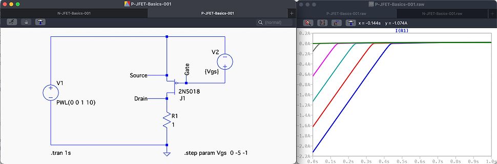
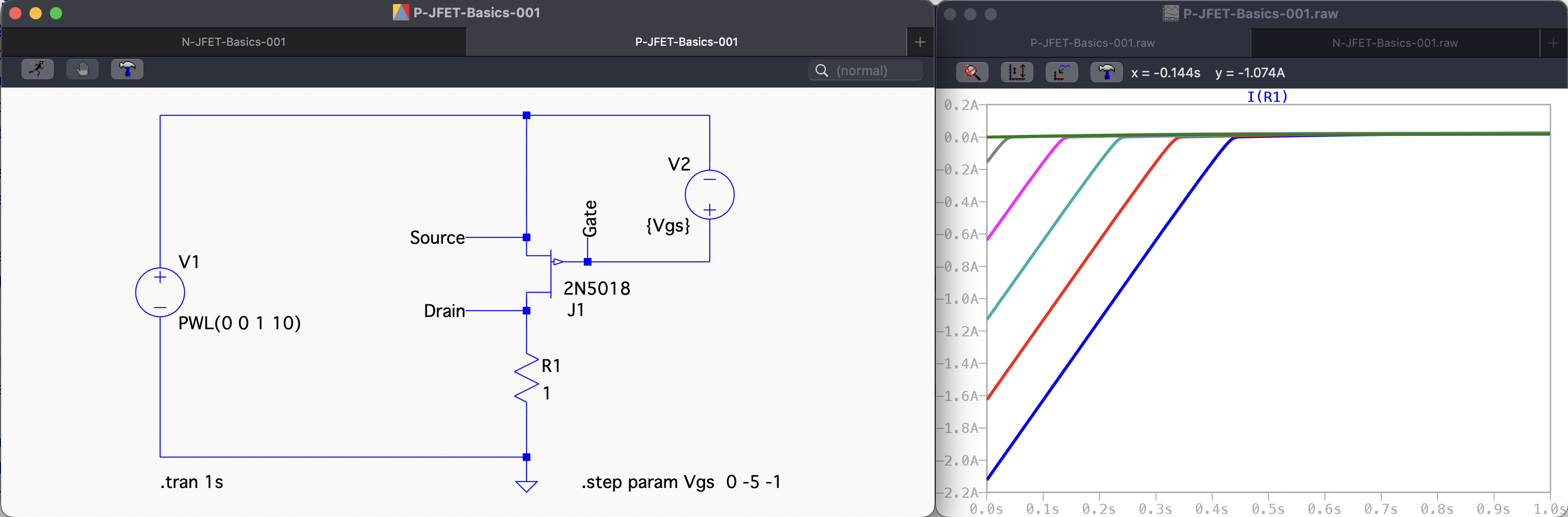
P-JFET-Basics-001 N-JFET-Basics-001 V2 Vgs Source Gate 2N5018 J1 Drain R1 PWL(0 0 1 10) .tran 1s .step param Vgs 0 -5 -1 0.2A 0.0A -0.2A -0.4A -0.6A -0.8A -1.0A -1.2A -1.4A -1.6A -1.8A -2.0A -2.2A x = -0.144s
in „JFET - Beschaltung“ · Analoge Elektronik und Schaltungstechnik · · Screenshots
-
Bild
Schaltplan und Kennlinie eines JFET-Transistors
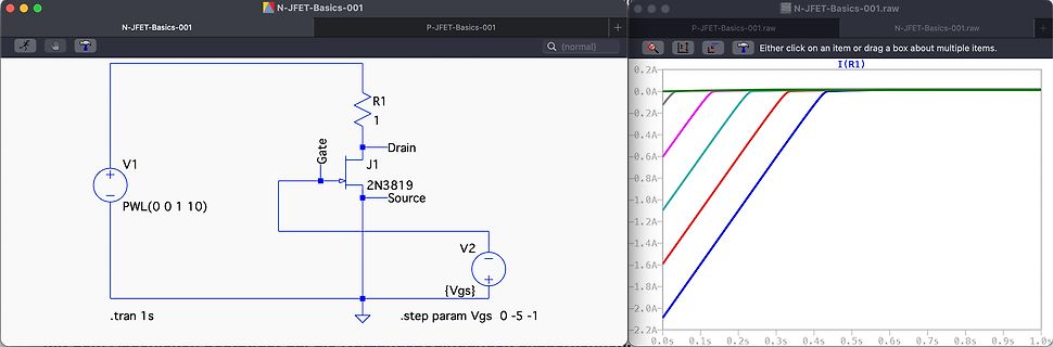
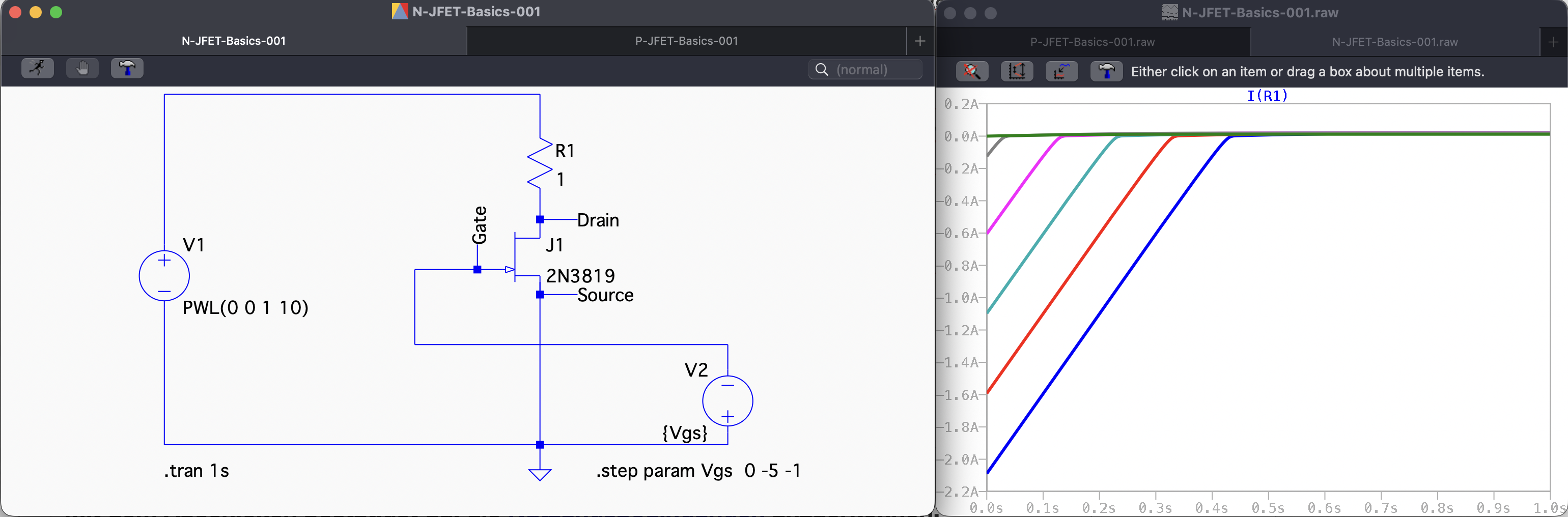
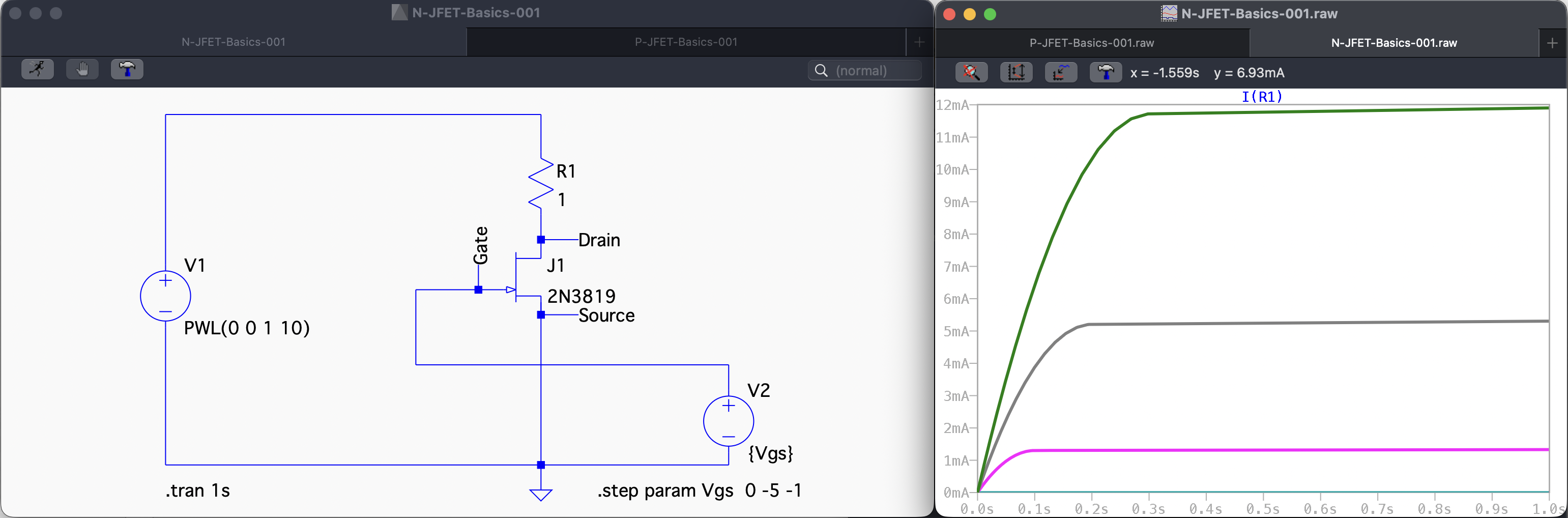
N-JFET-Basics-001 P-JFET-Basics-001 V1 R1 1 Drain Gate J1 2N3819 Source V2 {Vgs} .tran 1s .step param Vgs 0 -5 -1 I(R1) 0.2A 0.0A -0.2A -0.4A -0.6A -0.8A -1.0A -1.2A -1.4A -1.6A -1.8A -2.0A -2.2A 0.0s 0.1s
in „JFET - Beschaltung“ · Analoge Elektronik und Schaltungstechnik · · Screenshots
-
Bild
Schaltplan und Kennlinien eines N-JFETs
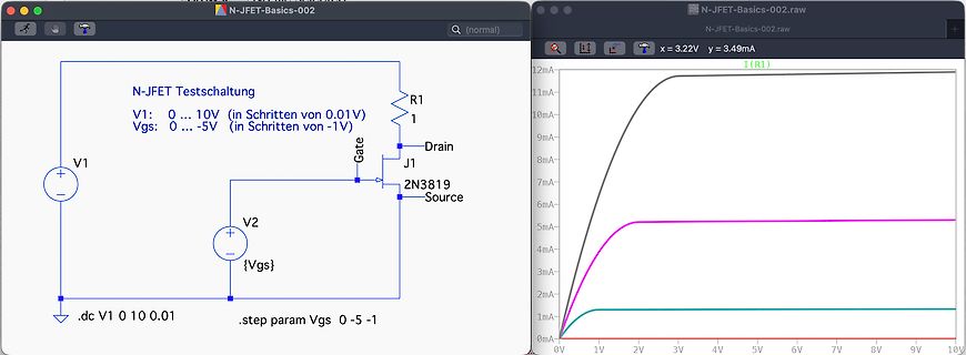
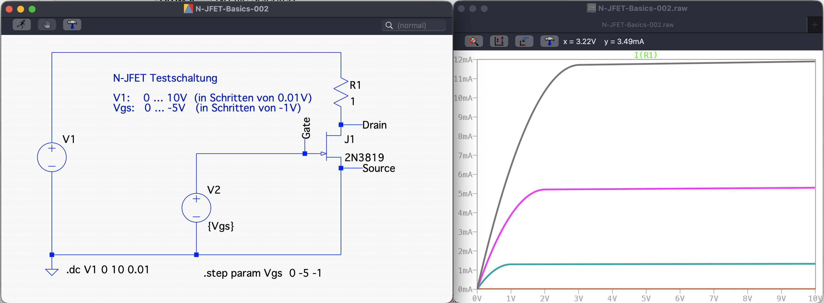
N-JFET-Basics-002 N-JFET Testschaltung V1: 0 ... 10V (in Schritten von 0.01V) Vgs: 0 ... -5V (in Schritten von -1V) R1 1 Gate Drain J1 2N3819 Source .dc V1 0 10 0.01 .step param Vgs 0 -5 -1 x = 3.22V y = 3.49mA
in „JFET - Beschaltung“ · Analoge Elektronik und Schaltungstechnik · · Screenshots
-
Bild
Schaltplan und Kennlinien eines JFET in Simulationssoftware
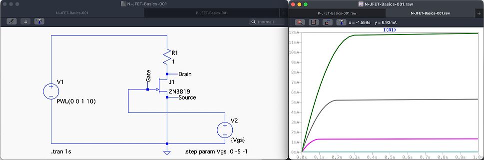
N-JFET-Basics-001 V1 R1 1 Gate Drain J1 2N3819 Source V2 {Vgs} .tran 1s .step param Vgs 0 -5 -1 x = -1.559s y = 6.93mA I(R1) 12mA 11mA 10mA 9mA 8mA 7mA 6mA 5mA 4mA 3mA 2mA 1mA 0mA 0.0s 0.1s 0.2s 0.3s 0.4s
in „JFET - Beschaltung“ · Analoge Elektronik und Schaltungstechnik · · Screenshots