Gast
#3189449
Hallo Leute,

ich spiele für mich privat momentan ein bisschen mit unter anderem
Ethernet und USB Geräten rum.

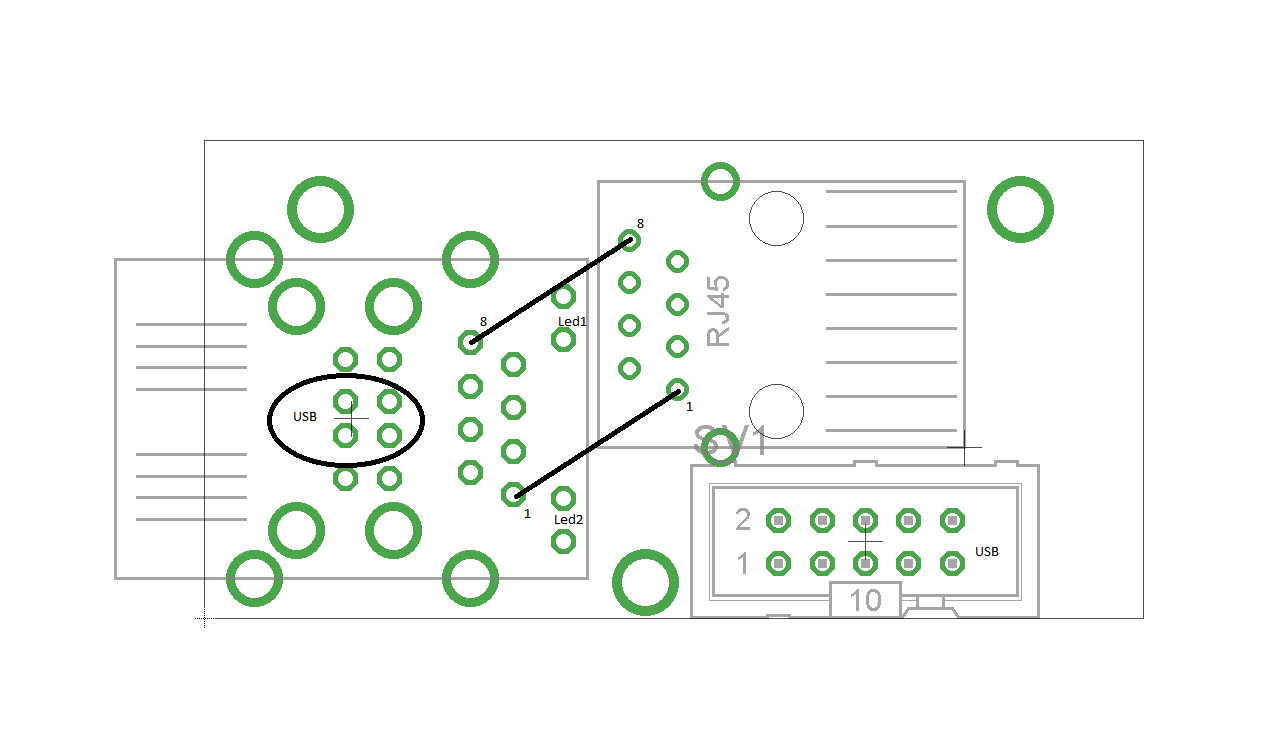
Ich wollte mir nun eine USB2 und Gigabitethernet adapterplatine routen.
Dass das nicht ganz so einfach wie SPI wird wahr mir schon klar...

Aber... wow, wirklich nicht einfach.


Also ich habe inzwischen einige design guides u.a. von Intel zu USB
durchgelesen.

Anscheinend ist sowas auf einer zweilagigen Platine schonmal unmöglich
wegen den differentiellen impedanzen. Soweit ich bis jetzt weiß 90 Ohm
zwischen den USB Signalen, 45 ohm zu masse.

Für Gigabit hab ich das hier:

1.) Route symmetrically as best as you can
2.) Avoid using vias for routing these traces: route a pair on the same
board layer
3.) Follow inter-pair (greater than 5x the height of the board
dielectric) and intra-pair (<10mil) distance guidance as given in the
layout checklist
4.) For gigabit designs, to achieve #3 easily, route two pairs on one
layer and the remaining two pairs on another layer
5.) Route on layers that are isolated to good grounds: don't route on
layer that is next to another signal layer <- avoids broadband coupling
6.) Differential pairs need to be length matched to within 50 mils...
They don't need to be exactly the same length
7.) Target 100 ohm differential impedance


Kann das einer? :-/ Krieg ich das hin mit der obigen platine? die is ja
wirklich mini einfach im vgl. zu dem was auf nem mainboard ist.

Danke!
Angehängte Dateien:
-
 usbrouting.png
(11 KB)
usbrouting.png
(11 KB)