Hallo,
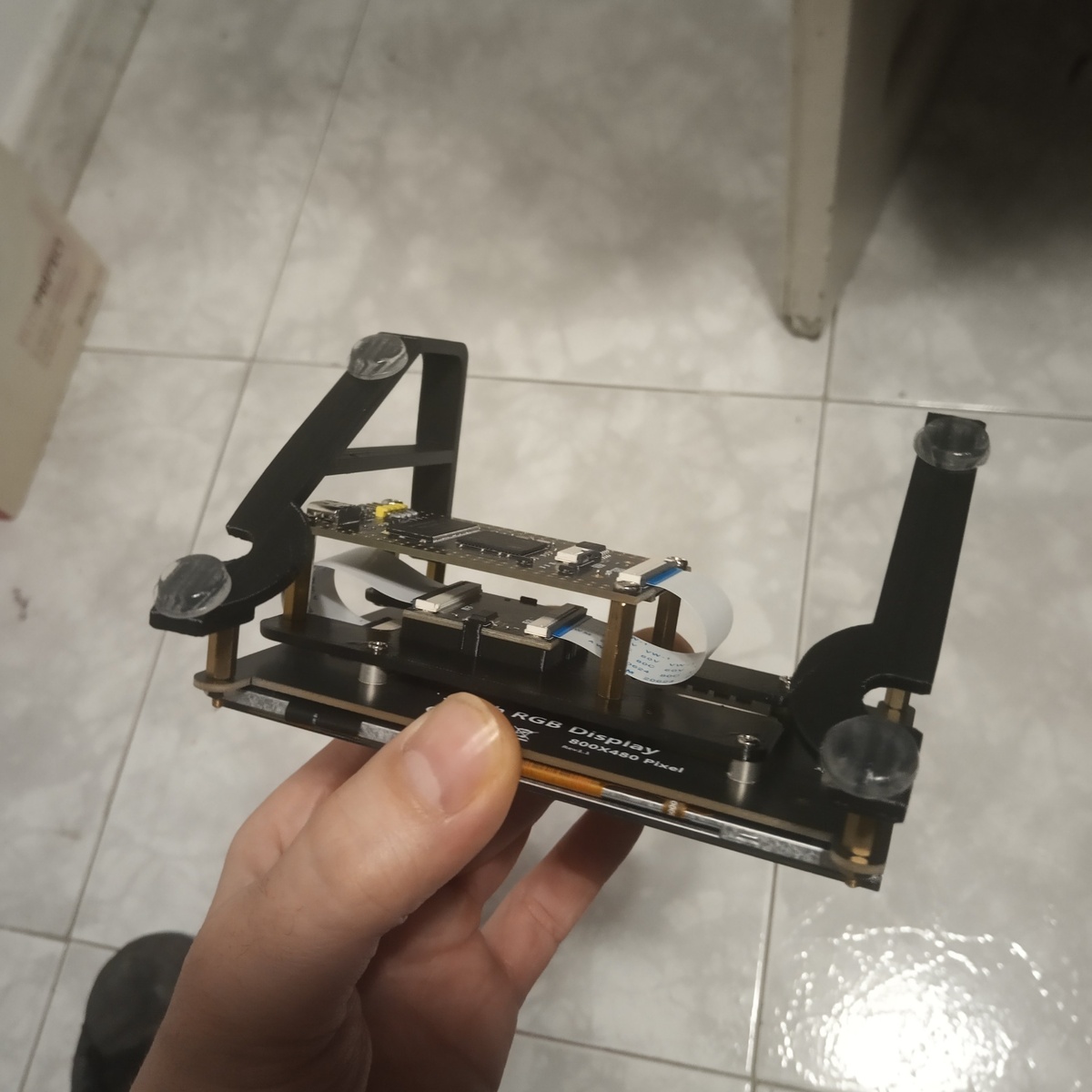
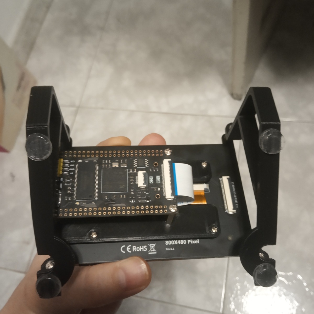
ich nehme hier gerade ein STM32H743 Board mit externem 32MByte SDRAM über FMC in Betrieb. Scheint alles zu funktionieren, das Ram lässt sich schreiben und lesen. Ich habe mir dazu ein kleines Testprogramm geschrieben:
1
DBG_log("\r\n -------------------- SDRAM 16 bit access -------------------\r\n");
Ist da wirklich so ein großer Unterschied zwischen Schreiben und lesen ?.
Hat vielleicht jemand ein ähnliches Board und kann das mit seinen Treibern nach vollziehen ?
Warum hat das nur auf den 16 Bit Zugriff eine Auswirkung ?
Ich brauche die 32MByte Ram als Messwertspeicher muss also nur schnell 32Bit Werte schreiben und kann sie später langsamer wieder auslesen.
Hätte mich trotzdem interessiert was da abläuft ...
Im FMC init wird das Timing für den Speicherzugriff eingestellt, wie
sieht das denn aus?
Wenn es beim abgeschalteten D-Cache Zugriff knallt dann wird vermutlich
ein clean/clear Cache aufgerufen, die muss man dann auch deaktivieren.
Sind die Caches default beim Start aktiviert ?
Da ist die ganze Zeit nicht passiert.
Könnte vielleicht auch sein, wenn ein eingeschalteter cache deaktiviert wird, das er vorher geleert werden muss ?
Wenn der Code von CubeMX generiert wurde dann ist der Cache in den CPU Einstellungen ein- oder ausgeschaltet, default ist da eingeschaltet.
Die manuelle Cache Pflege ist aber hauptsächlich bei DMA nötig, ist noch anderer Code für Ethernet oder SD Karte drin? Da können die herkommen. Sonst mal im Projekt nach SCB_ suchen.
Das Write schneller ist als Read sieht jedenfalls nicht plausibel aus.
Interessant, das ist glaube ich noch nicht in meiner Sammlung, muss mal nachschauen.
Beim DMA ist bekannt das man den Cache manuell pflegen muss, aber ich muss auch noch einen Fehler suchen bei dem Daten aus dem Flash nicht aktualisiert werden. Da bin ich mir auch sicher das es mit dem Cache zusammenhängt. Jedenfalls hat der starken Einfluß auf die Laufzeit.
Der Cache beim H7 ist sehr tückisch.
Wenn der Code von CubeMX generiert wurde dann ist der Cache in den CPU
Einstellungen ein- oder ausgeschaltet, default ist da eingeschaltet.
Die manuelle Cache Pflege ist aber hauptsächlich bei DMA nötig, ist noch
anderer Code für Ethernet oder SD Karte drin? Da können die herkommen.
Sonst mal im Projekt nach SCB_ suchen.
Das Write schneller ist als Read sieht jedenfalls nicht plausibel aus.
CubeMx setzt die caches "normalerweise" am Anfang der Main. Und dort habe
ich mit SCB_EnableICache(); / SCB_DisableICache(); und SCB_EnableDCache();/
SCB_DisableDCache(); herumgespielt.
Ist im Moment nur QSPI Flash (8Mb), USB CDC und 2 x SPI für ein ILI9488 TFT mit Touch drin.
CubeMx setzt die caches "normalerweise" am Anfang der Main. Und dort
habe
ich mit SCB_EnableICache(); / SCB_DisableICache(); und
SCB_EnableDCache();/
SCB_DisableDCache(); herumgespielt.
Ist richtig, das kann aber in CubeMX in den CPU Einstellungen gesetzt werden ob Enabled oder Disabled.
Bei Disabled darf man dann nicht die SCB_Invalidate oder SCB_Clear aufrufen, das könnte z.B. auch im USB Code drinstehen. Oder SPI wenn der mit DMA arbeitet. Es crasht also woanders.
Ich würde zunächst die Schreib-/Lesesignale mit dem Skope am SDRAM ansehen. Ggf. sind dort schon viele 'waitstates' vorhanden.
Alternativ eine Initialisierung ohne CubeMX schreiben, die sich vielleicht an anderer Stelle im Netz findet - zumindest als Grundlage.
CubeMx setzt die caches "normalerweise" am Anfang der Main. Und dort
habe
ich mit SCB_EnableICache(); / SCB_DisableICache(); und
SCB_EnableDCache();/
SCB_DisableDCache(); herumgespielt.
Ist richtig, das kann aber in CubeMX in den CPU Einstellungen gesetzt
werden ob Enabled oder Disabled.
Bei Disabled darf man dann nicht die SCB_Invalidate oder SCB_Clear
aufrufen, das könnte z.B. auch im USB Code drinstehen. Oder SPI wenn der
mit DMA arbeitet. Es crasht also woanders.
Ich würde zunächst die Schreib-/Lesesignale mit dem Skope am SDRAM
ansehen. Ggf. sind dort schon viele 'waitstates' vorhanden.
Alternativ eine Initialisierung ohne CubeMX schreiben, die sich
vielleicht an anderer Stelle im Netz findet - zumindest als Grundlage.
Und warum sollten diese "waitstates" nur beim lesen und nicht beim schreiben auftauchen ?
CubeMx initialisiert ja nur die FMC Register die Ram Initialisierung und das schreiben und lesen ist von dem Code für STM Disco Boards abgeschaut und angepasst.
A.) ICache beschleunigt mein FMC Test beim schreiben aber nicht beim lesen, DCache hat darauf keinen Einfluß.
B.) Irgend ein anderes Teil in meinem Programm aktiviert den ICache zwischen dem 16 Bit und dem 8 Bit Test, das erklärt warum das 8 Bit Schreiben immer schnell ist.
On Board ist keiner aber es lässt sich extern aus dem genannten Grund auch keiner anschließen. Den FMC PIN könnte man umlegen aber dazu müsste man den Hersteller finden und überzeugen ;-) Und BGA fädeln macht auch keinen Spaß.
Ok, ja Schade, so externe ULPI Boards gibt es ja auch für ein paar Euro. Es gibt die STM Disco Boards mit zusätzlichem Speicher und Display, aber die sind leider ein ganzes Stück teurer.
Ok, ja Schade, so externe ULPI Boards gibt es ja auch für ein paar Euro.
Es gibt die STM Disco Boards mit zusätzlichem Speicher und Display, aber
die sind leider ein ganzes Stück teurer.
Also On Board sind:
32MByte RAM, 8MByte QSPI Flash, SD-Karten Slot, Kamera Anschluss, LCD Schnittstelle SPI und Parallel dazu noch ca. 80 Pin über Steckerleiste.
Das sehe ich auch so, aber warum passt die Schreibschleife in den Cache
und die Leseschleife nicht ?
Beide passen da rein, mit dem Unterschied, daß beim Schreiben zunächst in ein FIFO des FMC geschrieben wird bzw. werden kann. Gepufferte Daten können dann schneller gespeichert werden. Beim Lesen muß immer gewartet werden, bis das SDRAM die Daten auch geliefert hat.
Darum würde ich mir ansehen, wie die Zugriffe auf das SDRAM aussehen. Läuft alles in einem Rutsch, was kaum zu glauben wäre, oder wird Byte für Byte mit vielen Taktzyklen und womöglich noch mit Pausen gelesen.
Aber gut, das interessiert nur, wenn man die Zugriffe möglichst schnell ausgeführt haben möchte.
Darum würde ich mir ansehen, wie die Zugriffe auf das SDRAM aussehen.
Läuft alles in einem Rutsch, was kaum zu glauben wäre, oder wird Byte
für Byte mit vielen Taktzyklen und womöglich noch mit Pausen gelesen.
Aber gut, das interessiert nur, wenn man die Zugriffe möglichst schnell
ausgeführt haben möchte.
Ach Michael ich bin jetzt 75 Jahre, halb blind und zittrig ;-).
Da würde ich ungern Drähtchen an den BGA Chip oder das Ram zum messen löten. Falls ich es mal schneller brauche gibt es auch noch den Schreib/Lese Burst-Mode und kann vielleicht ja auch noch an den Parametern drehen.
QSPI geht auch
-------------------- QSPI Test -------------------
Ach Michael ich bin jetzt 75 Jahre, halb blind und zittrig ;-).
Da würde ich ungern Drähtchen an den BGA Chip oder das Ram zum messen
löten.
Ja, ich verstehe. Man kann unter Umständen auch viel kaputt machen.
Deinen zuerst genannten Wert von rund 180 MB/s fand ich nur so verlockend, daß das dann gleich die Messlatte für alle Zugriffe sein sollte ;-)
Für Messwerspeicherung reicht es wohl allemal.
ich nehme hier gerade ein STM32H743 Board mit externem 32MByte SDRAM
über FMC in Betrieb.
hast du zu diesem Board mehr Infos? Ich konnte nicht widerstehen und habe es auch gekauft.
Da ist schon eine Software drauf, am UART am Programmer Anschluss bekommt man einige Logs. Den richtigen Zeichensatz habe ich nicht gefunden, aber es scheint ein Test des SDRAM zu sein, ein LCD mit Touch sowie ein Kameramodul wird gesucht.
Der Kameraanschluss hat leider 20 Pins statt wie die 24 bei der ESP Cam, die Module passen so direkt nicht. Auch für das LCD mit RGB muss ich mir einen Adapter bauen, habe da nur was mit 6 Bit RGB.
Lesebefehle auf einer CPU sind immer langsamer als Schreibbefehle. Wenn etwas geschrieben werden muss, dann kann die CPU Daten und Adresse auf den Bus schicken und einfach weiter machen, sie muss normalerweise nicht darauf warten, dass die Daten im Ziel angekommen sind. Beim Lesen hingegen muss zuerst eine Adresse abgesetzt werden, dann wird auf die Daten gewartet und dann gehts erst weiter. Das kann man zwar ein bischen in der Pipeline verstecken, hilft aber nix wenn man von langsamer Peripherie (z.B. SDRAM liest) Deswegen gibts ja Caches.
Allerdings erscheint mir hier der Unterschied viel zu groß. Zumal der FSMC eine Read-Fifo hat, die genau bei solchen Sequentiellen Reads helfen sollte die Wait-States zu minimieren.
Ausnahme zu der Regel oben: Speicherbereiche die als "strongly order" markiert sind. Da muss der Zugriff komplett fertig sein, bevor der nächste gemacht wird.
Möglicherweise ist die MMU/MPU nicht richtig eingestellt so das SDRAM nicht als "Normal" memory getagt ist.
Wie ich zu dem Board gekommen bin hat eine kleine Vorgeschichte.
Zuerst hatte ich ein STMh750 Board gefunden und gleich 2 bestellt. Leider nur 128Kb Flash intern, aber 8Mbyte Flash on Board.
Dann habe ich das STM32H743 Board gefunden ohne externes RAM ( 1 bestellt).
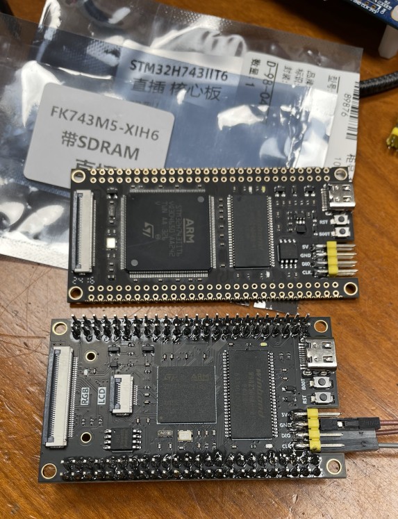
Als nächstes ein STM32H7 Board mit externem RAM. MCU im FP Gehäuse ( 0 bestellt). Und dann habe ich dieses Board gefunden mit MCU im BGA Gehäuse. Nachdem ich ein Schaltbild dazu gefunden hatte. (2 bestellt).
Den QSPI (für das H750) Treiber habe ich von irgendeiner chinesischen Seite und die Kommentare in englisch übersetzt. Der SDRAM Treiber ist einem Disco Board nachempfunden. Das ioc File für CubeMX ist gewachsen ;-)
Mein ILI9488 LCD und der Touch XPT2046 laufen über SPI5 und SPI6.
Viel mehr läuft noch nicht.
Am 743 Board ohne externes Ram hängt im Moment ein 3300 ULPI Board, funktioniert aber noch nicht.
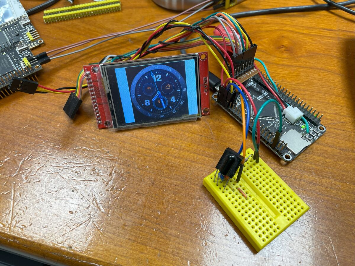
Das H743 Board ohne ext. RAM habe ich auch, DevEBox, Ver.2.0. Da habe ich ein Display mit lvgl dran und mal q'd IRMP zum Testen eingebaut. Die sind recht gut, haben aber eben kein ext. RAM.
Von den H743 mit SDRAM habe ich jetzt auch beide Versionen, die sind durch die großen H743 mit den vielen Pins auch interessant. Da möchte ich auch ein RGB Display anschließen.
Bei Ali habe ich mehrere Händler für diese Boards gefunden, einer (Online-parts Store) hat auch Varianten mit Display sowie das passende Kameraboard.
Ich hatte die in einem gekauft, den Link zum Schaltplan haben die mir auf Anfrage innerhalb von 10 Minuten geschickt, aber nichts zur Demo Software.
Deine Adapter mit VG Leiste für die doppelreihigen Pinheader sind interessant :) Ich habe lange Pinheader eingelötet die von oben und unten kontaktiert werden können, die sind für so Testaufbauten auch praktisch.
Ich habe dir mal alles was ich so für das Board habe gezippt.
Mit dem CubeMx ioc File kannst du dir ein make Projekt generieren und dann die QSPI und SDRam Files einfügen.
Das ioc ist mit dem aller neuesten CubeMX 6.12.1 und FW H7 V1.11.2 erzeugt, da ist aber ein Bug und das erzeugt Linkerscript funktioniert nicht. Ich habe ein funktionierendes hinzugefügt.
Im Excel Sheet steht die Pinbelegung.
Wenn du auch noch die Tests und Debug-Ausgabe an UART1 brauchst sag bescheid.
Danke,
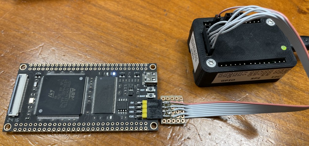
habe mir gerade einen Adapter für den STLink V3 gebaut. Bekomme aber
keine Verbindung zum Target, bei beiden Boards die gleiche
Fehlermeldung.
1
> 22:48:33 : ST-LINK FW : V3J13M4
2
> 22:48:33 : Board : STLINK-V3MINI
3
> 22:48:33 : Voltage : 3.30V
4
> 22:48:33 : Error: No STM32 target found! If your product embeds Debug
5
> Authentication, please perform a discovery using Debug Authentication
6
>
Debug Authentication hat der H7 soweit ich weiß aber nicht.
Kenn ich auch nicht .. ich benutze hier Stlink v2.1 von den Nucleo Boards und auf JLink umgeflashed oder einen JLink EDU mini. Versuch mal mit dem St-Programmer eine Verbindung zu finden.
es lag an meinem Adapter, Verbindung zwischen Ober- und Unterseite bei einem Pin. Als ich nur die Buchse aufgelötet hatte, da habe ich es noch durchgemessen und es war ok. Mit Kabel zum STLink habe ich nicht mehr gemessen...
Mit dem CubeProgrammer unter WSL2 bekomme ich jetzt die Verbindung, mit der Windows Version nicht, obwohl ich die bisher schon unzählige Male benutzt habe. Ich probiere morgen weiter, jetzt habe ich keinen Nerv mehr.
Doch, jetzt klappt es auch unter Windows. Hurra, es kann weitergehen. Morgen.
ja, der SWD Anschluss ist bei beiden gleich. Ich wollte erst ein blinky auf diesem Board ans laufen bekommen. Dieses hat auch irgendeinen Code drauf, eine blaue LED blinkt langsam, aber über die serielle kommt nichts raus. Am USB-C macht das einen virtuellen COM Port auf, aber auch da kommt nichts. Ist eventuell ein Bootloader drauf.
Speculative data reads and speculative cache linefills are never made to
Device memory addresses.
Jetzt habe ich mal zum Spaß für den SDRAM Bereich den Caches enabled und lande dann beim Zugriff im memory fault handler. Das scheint die falsche Schraube zu sein ;-)
ja, falsche Cache Einstellungen nimmt er schnell übel.
Ich habe mein Adapterkabel verbessert, durch einen gecrimpten Stecker ersetzt. Weiß nicht warum ich das nicht sofort so gemacht habe...
Trotzdem war die Verbindung nicht stabil, mal ging es und meist nicht, mit verschiedenen Fehlermeldungen. Dann fiel mir ein das der USB-C Hub an meinem Dell Laptop rumzickt, die Verbindung zum Headset ist darüber z.B. auch schlecht. STLink an einen anderen, USB 2.0 Hub eingesteckt und zack lief es.
Jetzt hangele ich mich auch weiter.
hier ist noch eine Kleinigkeit, da sollte write speed stehen (beim 8 Bit Test).
Mein Blinky bzw. printf auf Konsole läuft auch, ich baue das Ganze mit Mbed. Die Boards gibt es dafür natürlich nicht, das ist erst die meiste Arbeit die einzupflegen.
Für den fmc Code wollte ich dein .ioc öffnen, dazu musste ich noch einige Updates installieren. Ich hoffe es schreddert nicht meine wichtigen Projekte...
Speculative data reads and speculative cache linefills are never made to
Device memory addresses.
Jetzt habe ich mal zum Spaß für den SDRAM Bereich den Caches enabled und
lande dann beim Zugriff im memory fault handler. Das scheint die
falsche Schraube zu sein ;-)
Ja klar geht der in Fault, der Fehler hier ist zunächstmal das der Speicher als "Device" getaggt ist. "Device" Memory kann bzw darf nicht gecached sein. SDRAM sollte "Normal" sein. Dazu kommt, das beim STM32H7 der Bereich nicht "Shareable" sein darf, weil dann der D-Cache abgeschaltet wird. (Dem fehlen die Units um "Shareable" zu synchronisieren)
Speculative data reads and speculative cache linefills are never made to
Device memory addresses.
Jetzt habe ich mal zum Spaß für den SDRAM Bereich den Caches enabled und
lande dann beim Zugriff im memory fault handler. Das scheint die
falsche Schraube zu sein ;-)
Ja klar geht der in Fault, der Fehler hier ist zunächstmal das der
Speicher als "Device" getaggt ist. "Device" Memory kann bzw darf nicht
gecached sein. SDRAM sollte "Normal" sein. Dazu kommt, das beim STM32H7
der Bereich nicht "Shareable" sein darf, weil dann der D-Cache
abgeschaltet wird. (Dem fehlen die Units um "Shareable" zu
synchronisieren)
Nachtrag bei dem Wert bin ich mitr nich sicher MPU_REGION_SIZE_32MB
sind mit size Bytes gemneint oder hängt das von der RAM busbreite ab ?.
(32M x16)
Wenn Bytes gemeint sind müsste es auf 64 ist ein 256Megabit Ram
beide liefen den gleichen Fehler, beim IIT6 könnte die SDRAM Belegung natürlich anders sein, habe ich jetzt nicht verglichen.
Das low level hardware Init wird noch fehlen.
Aber ich muss langsam Schluss machen für heute.
beide liefen den gleichen Fehler, beim IIT6 könnte die SDRAM Belegung
natürlich anders sein, habe ich jetzt nicht verglichen.
Das low level hardware Init wird noch fehlen.
Aber ich muss langsam Schluss machen für heute.
Anbei mal mein Core verzeichnis da kannst du morgen vergleichen.
Das BoardTest() fehlt noch. Aber meine beiden Init calls sehen erstmal gut aus.
Die beiden Board Versionen haben das SDRAM natürlich anders angeschlossen, wenn ich das so übernehme dann läuft es nur das BGA Board. Aber das müsste der einzige Unterschied sein um den Code auf beiden zu nutzen.
Ich kämpfe noch mit dem Debugger, das klappt in meiner Umgebung (VSCode mit Cortex-Debug Extension) noch nicht.
Das messen der SDRAM Signale ist auch schwierig, die liegen nicht an den Pinheadern.
Du brauchst einen Ordner ".vscode" in deinem Projekt und darin ein File launch.json mit folgendem Inhalt. Musst du natürlich auf dein Projekt und deine Pfade anpassen
Habe mir mal das China zeug heruntergeladen. Der Hersteller des Boards scheint "Fanke electronics" zu sein. Habe die Firma aber nicht im Internet gefunden.
Fanke könnte eine Unterdivision von Guilin Technologies sein, der Name stand ein einem Dokument in Chinesich über dem Fanke Schriftzug. Fanke stand auch in dem Schaltplan vom IIT6 Board.
Mit dem Cortex-Debug habe ich schon eine Menge gemacht, auch andere H743 laufen damit. Die Konfig wird hier jetzt von Mbed-CE generiert, das geht über arm-gdb und STLinkGDBServer. Den servertype stlink probiere ich auch nochmal.
Es hatte auch anfangs mal geklappt, dann habe ich die Target Anpassung für das Board sauberer gemacht und seitdem geht es nicht mehr, das bekomme ich aber hin.
Der STLinkGDBServer bekommt eine Verbindung, hängt sich dann aber auf beim lesen von Registern auf. Da ist die Meldung 'CM4 failed' komisch, das ist ja ein CM7 single core.
1
CM4 Failed to read all registers
2
ST-LINK device status: Failed to get status, Target not responding, retrying... 19
Das messen der SDRAM Signale ist auch schwierig, die liegen nicht an den
Pinheadern.
Messen? Du hast ein Oszi mit 1GHz Bandbreite? (Nicht Sampling Rate!) Wenn Nein, dann vergiss das mit dem Messen mal ganz schnell wieder. Bei den Taktraten muss man sich auch langsam um Signallaufzeiten, Impedanzen (und Reflektionen) Gedanken machen. Insbesondere da SDRAM noch "Single-Ended" ist. z.B. sollte auch bei 100MHz die Clock Leitung zumindest länger als die Daten/Adressleitungen sein.
Und wer jetzt meint das wäre übertrieben. Ja, für den Schreibtisch/Bastler mag das ohne all das gehen. Wenn man sowas in einem Schaltschrank mit erweitertem Temperaturbereich packt wo auch noch andere Sachen unterwegs sind... viel Spaß. Wir hatten schon Rückläufer wegen ungünstigem Layout. "Geht" heißt halt nicht "geht immer".
Mit dem Oszi würde ich die CS / RAS / CAS Signale sehen wollen ob sich da überhaupt etwas tut, also die Konfiguration gelaufen ist.
Es gibt andere Boards wo zusätzliches RAM Optional ist und die Signale daher auch extern verfügbar sind. Hier ist es fest auf dem Board und da macht es natürlich Sinn diese hochfrequenten Signale nicht unnötig über das Board zu führen.
Mit dem Oszi würde ich die CS / RAS / CAS Signale sehen wollen ob sich
da überhaupt etwas tut, also die Konfiguration gelaufen ist.
Es gibt andere Boards wo zusätzliches RAM Optional ist und die Signale
daher auch extern verfügbar sind. Hier ist es fest auf dem Board und da
macht es natürlich Sinn diese hochfrequenten Signale nicht unnötig über
das Board zu führen.
Da sitzt ein STM32H7 in der Revision V drauf, der läuft mit 480 MHz das bedeutet das Ram läuft mit 120 MHz. Deshalb hatte ich ja das BGA Board gewählt. Board mit Ram und parallel Stichleitungen zu den Pin-Headern bringen doch nur zusätzliche Leitungskapazitäten und Kopplung.
Da sitzt ein STM32H7 in der Revision V drauf, der läuft mit 480 MHz das
bedeutet das Ram läuft mit 120 MHz. Deshalb hatte ich ja das BGA Board
gewählt. Board mit Ram und parallel Stichleitungen zu den Pin-Headern
bringen doch nur zusätzliche Leitungskapazitäten und Kopplung.
Ja, und solche parasitären Kapazitäten bei diesen Frequenzen gilt es zu vermeiden, denn die werden schneller zuschlagen als irgendwelche Signallaufzeitdifferenzen.
Ich habe bei dem Board noch Probleme mit dem Debugger (STLinkV3):
Wenn ich durch SetSysClock() steppe, dann verliert der Debugger die Verbindung nach __HAL_PWR_VOLTAGESCALING_CONFIG(PWR_REGULATOR_VOLTAGE_SCALE1);
mit der Meldung:
"Failed to read registers from target".
Zu diesem Problem habe ich zwei Beiträge in der STCommunity gefunden, einmal sollen Debug Einstellungen geholfen haben, die ändern hier aber nicht. Dann eine andere, externe Spannungsversorgung. Damit komme ich ein paar Schritte weiter, richtig zuverlässig ist es aber immer noch nicht. Stromversorgung habe ich über eine angzapfte VUSB zum Programmierstecker und da auch zwei verschiedene USB probiert, die liefern 5.0 V / 4,65 V über ext. Hubversorgung.
Dann die 5V extern von einen LaborNT eingespeist, damit geht es etwas besser, aber eben nicht 100 %.
Der Fehler tritt gleichermaßen auf in der CubeIDE (in WSL2) sowie mit VSCode, was aber auch arm-none-eabi-gdb und STLINK GDB Server nutzt.
@Hans-Georg: könntest du das auch mal probieren, einen BP in SetSysClock setzen und mit Step Over da durch gehen?
ok, Danke.
Ich habe die CubeIDE im WSL2 laufen und auf 1.16.1 aktualisiert. Auch VSCode läuft im WSL, ich werde es noch mal auf einem Rechner ohne WSL testen um das ohne die usbidp Brücke zu testen. Das hat allerdings immer sehr zuverlässig funktioniert, auch mit anderen H7.
ok, Danke.
Ich habe die CubeIDE im WSL2 laufen und auf 1.16.1 aktualisiert. Auch
VSCode läuft im WSL, ich werde es noch mal auf einem Rechner ohne WSL
testen um das ohne die usbidp Brücke zu testen. Das hat allerdings immer
sehr zuverlässig funktioniert, auch mit anderen H7.
Schalte mal die Taktfrequenz auf 400Mhz runter vielleicht sind das auf V umgelabelte Y Revisionen.
Hi guys,
sorry for my english post but as an Italian person my languages knowledge include a lot of local dialects but, unfortunately, not the German. And I totally refuse to include an answer translated by Google.
I was reading by days this thread looking at your development on FK743M5-XIH6 board, which I've bought in the meanwhile.
I was doing some test on the SDRAM maximum achievable speed, running a mix of Fanke code and above one and, despite the values of the first post, I got a speed under 100MB/s!
1
-------------------- SDRAM 16 bit access -------------------
I’m not at my PC right now, but the SDRAM timing settings look the same as mine or what Hans Georg has published here.
Have you checked the clock tree if the clock settings are ok? The values in your snippet look also ok, but e.g. the FMC clock source could be wrong.
I can check your code later.
Your MPU Config is not optimal. Your setting only enables caches for SDRAM but not for instruction memory. Thus the instructions are not cached an need to be loaded every time from flash. (Flash is slow, the maximum speed of internal flash of this device is 70MHz)
Please note the settings above were two MPU regions are configured. The first MPU region is for caching the instructions and the second is for caching SDRAM. Also the SDRAM Region should be set to "Bufferable", this improves Write Speed.
You should also check that your code is compiled with optimizations enabled and not in debug mode without any optimizations. ("Optimization Level" should be set to -O2 or -Os)
You should also check that your code is compiled with optimizations
enabled and not in debug mode without any optimizations. ("Optimization
Level" should be set to -O2 or -Os)
Der Unterschied hat mich mal interessiert hier der Vergleich:
It's been years since I didn't get in touch to such a collaborative forum, kudos to all of you.
Thanks, furthermore, for the info provided. I've made some tests and results follow below. Actual configuration is -O1 + D/ICache Enabled + MPU on SDRAM (not shareadble, cacheable, not bufferable). ioc attached to this post.
1
-------------------- SDRAM 16 bit access -------------------
SDRAM 8-Bit data validation pass, elapsed time: 168 ms
9
Waiting for reboot...
Code optimization seems to play an important role, -O1, -O2, -O3, -0fast seems to get all the same (fast) results, above all -O1 get a ten of MB more in reading on 16bit; others configuration get slight worse speed.
Enabling ICache and DCache also is fundamental. Turning off ICache slows the 8bit read to 13.40 MB/s. Turning off DCache slows both 8 and 16 bit reads to 23.05 MB/s and 15.01 MB/s.
Configuring MPU on 0x8000000 seems to have no substantial effect at all if I\DCache are disabled.
Configuring MPU on SDRAM seems to have an important effect, but, enabling the bufferability seems to have no effect at all. Enabling the shareability when DCache is disabled get slow reading speeds: both 22.47 MB/s.
My actual problem is, since I use SDRAM to store "slow" data (10Sa/s ADC) which have to be used for "very fast" analysis (RMS calculation), I have to enhance reading speeds which still get slow if compared to reading. I've understand what Andreas said above (31.10), but I have seen no additional answers so I was wondering if any of you get the problem solved.
The test loop is very short with a few cpu cycles, and so a difference of +/- 1 cycle caused by the optimization has a big effect on the result. The loop should also fit into the instruction cache, which makes it fast or much slower when it gets larger and does not fit.
So I think for a real application these speed results have a limited relevance.
My actual problem is, since I use SDRAM to store "slow" data (10Sa/s
ADC) which have to be used for "very fast" analysis (RMS calculation), I
have to enhance reading speeds which still get slow if compared to
reading. I've understand what Andreas said above (31.10), but I have
seen no additional answers so I was wondering if any of you get the
problem solved.
Hi Luca. Are you sure its the SDRAM and not you algorithm by itself? RMS sounds like Sqare-Roots (Slow), Multiplication & Additions (Should be fast). You could also consider an improved alogrithm. For instance if you have a moving average algorithm, one approach could be to store the sum in a single variable and each sampled value in a ring buffer (length = number of samples). When a new sample comes in, you take the sum, subtract the value of current ring buffer index, add the new sample to the sum and store the new sample to ringbuffer index, increment ring buffer index. (Divide sum by number of samples to yield result). Thus it does not matter if your moving avg is 100 or 100000 samples. The update is always constant in time.
Kannst Du mir sagen, mit welchem Frequenz bei Dir das QSPI angesprochen wird? Auf meinem selbsterstellten Board komme ich nur bis 40 MHz SCLK. Leider habe ich die Längswiderstände im QSPI nicht layoutet, aber auf dem chin. Testboard, von dem Du den Schaltplan gezeigt hast, sind auch keine drin.
Kannst Du mir sagen, mit welchem Frequenz bei Dir das QSPI angesprochen
wird? Auf meinem selbsterstellten Board komme ich nur bis 40 MHz SCLK.
Leider habe ich die Längswiderstände im QSPI nicht layoutet, aber auf
dem chin. Testboard, von dem Du den Schaltplan gezeigt hast, sind auch
keine drin.
Danke, Axel
Wünsche auch allen ein gutes neues Jahr.
Hallo Axel, QSPI hängt am HCLK3 (240 MHz) und der Prescaler steht auf 1 ( div 2) also läuft es mit 120 MHz.
Und die GPIO sind auf GPIO_SPEED_FREQ_VERY_HIGH initialisiert.
Hi Luca....You could also consider an improved alogrithm. For instance if
you have a moving average algorithm, one approach could be to store the
sum in a single variable and each sampled value in a ring buffer (length
= number of samples).
That changed really the scenario, the solution is kinda perfect but, for completely other reasons, the solution still is not working.
Let me expand the scenario to better explain the project I'm working on: A 4ch 1MSa/s 16bit acquisitor which outputs via USB the RMS value of last 100ms window every 100ms.
So I've setted up a:
SDRAM: We've already talked in depth about this.
ADC1:
Resolution: ADC 16-bit resolution,
Scan Conversion Mode: Enabled,
End Of Conversion Selection: End of sequence of conversion
Conversion Data Management Mode: DMA Circular Mode
Enable Regular Conversions: Enable
Number of Conversion: 4
External Rrigger Conversion Edge: Trigger detection on the rising edge
..setted up the 4 Ranks with channels 4-5-1-19
...setted up the DMA Settings as: DMA1 Stream 0 Circular, Memory\Word, Priority Very High
...if(hadc1.Init.NbrOfConversion>0){//<-Optimization delete the unused conversions when configured via .IOC
3
tempval=*(__IOuint16_t*)(Ablock+2*i);
4
Asum-=tempval*tempval;
5
tempval=AD_RES_BUFFER[0];
6
*(__IOuint16_t*)(Ablock+2*i)=tempval;
7
Asum+=(uint64_t)tempval*tempval;
8
}
9
10
...(doesthesamefortheother3channels)...
11
12
//Advance index
13
i=(i==Xcnt-1)?0:i+1;
14
...
15
}
In the main:
1
...
2
if(PrintFlag){//todo Print data on TIM14 interrupt (10Hz)
3
sprintf(text,"A:%f,B:%f,C:%f,D:%f\r\n",
4
(q*sqrt(Asum/Xcnt)),
5
(q*sqrt(Bsum/Xcnt)),
6
(q*sqrt(Csum/Xcnt)),
7
(q*sqrt(Dsum/Xcnt))
8
);
9
usb_print(text);
10
11
PrintFlag=0;
12
}
I was so happy with the results on 2 channels, but when I scaled up to 4 channels, everything stopped working...
I'm attaching the full code actually configured for 2ch A:R1:ADC1.4 / B:R2:ADC1.5, please give it a try enabling 3 or 4 on "Number of Conversion" and configuring ranks with ADC1.1 or ADC1.19 (Already configured) and you'll see strange behaviours I really can't debug! :(
It has been two days trying to change configurations and code with no success, I'm kinda desperate.
It has been two days trying to change configurations and code with no
success, I'm kinda desperate.
I did not yet check you project in detail but: I assume 4 Channels, each with 1 MS/s is just too fast what this CPU can handle in such a design. As of your algo I assume these are about (10 to 20) instructions times 4 channels. This alone costs about 80MIPs. I further assume "HAL_ADC_ConvCpltCallback" run in some interrupt context which is somehow abstracted in some layers of the STM Cube code. This abstraction costs performance in addition to interrupt entry itself. (For instance a Cortex M7 CPU has 12 clocks latency for ITCM Code in optimal situation, thus a 100 MHz clocked Cortex M7 can handle no more than about 8 Million Interrupts/s when the handlers are empty and CPU is not doing anything else) I would assume in your design the interrupt handling costs again something in the order of 10 to 100 MIPs.
What you can do is use a different DMA Buffer scheme: Since you only look at 10 Hz intervals, an idea would be to process data in blocks:
Each DMA Buffer contains more than one sample/per channel: E.g. 128 Entries 4 Samples per Entry (one per channel). Thus you get 1MS/s / 128 ~ 8 kHz Interrupt rate. You process 128 Samples en block per channel. This saves you from wasting CPU time with interrupt entry / leave. You can even optimize the summing since you only need to store one sum per 128 elements. You use two dma buffers, one is filled by ADC/DMA, the other is processed. (Double buffer scheme)
Just google about STM32, ADC & Double buffer will show some examples how to do that.
Hello everyone
After I visit this post sometimes and I beneficied to your comments and files.
I know so this post is only for SDRAM but... I don't find another references for tihis board, so I upload my project for FK743M5 board raw for gratitude in case anyone wants to take advantage of something.
The project contains:
SDRAM
QSPI + .stldr
LTDC
CDC
Soft I2C for touch
Screen config for LCD 5inc
I've loaded your .elf files, but I get only
'15:23:30.249> Address: 0x0 Data:' over the USB serial.
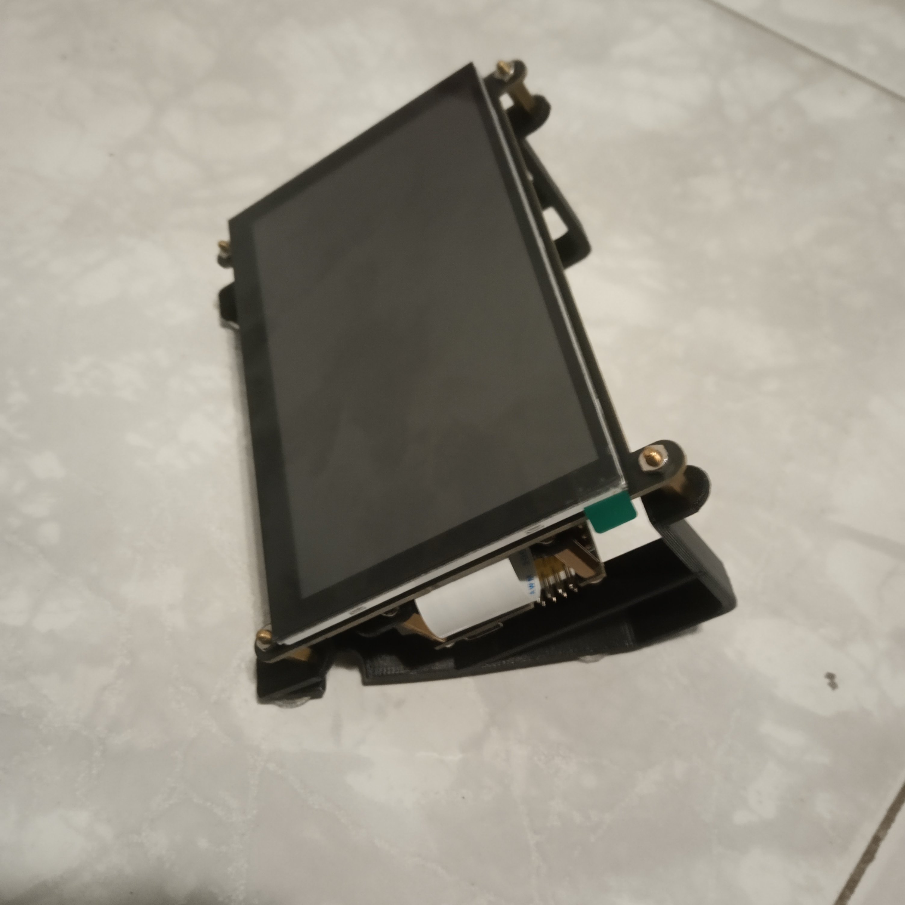
So it looks like your display is different, I have the 5" display that comes bundled with the FK boards. It has a GT911 multitouch controller, so that seems to be different.
I have added Mbed Suspport for this Board and display and lvgl is running fine on this board due to a lot of RAM.
edit:
when I remove the I2C read, the it works, also your logo is displayed on the screen.
Thanks for testing the code, in relation to the usb.
It may be that it needs to be configured in ?
Project Properties > Build > settings > misc > Other flags.
Add: -u printF_float
I still have to make the library for the FT5426 driver but the soft I2C communication already works. This driver is also 10 touch points.
The screen works with the adapter from the previous link, also if you can put a 7 inch screen.
The final intention is also to run LVGL, I really believe in the author's project.
Greetings.
PD: SDRAM addresses do not correspond to sector sizes.
This display adapter is nice, have not seen it before. The FK boards have a non standard pin assignment for the LCD screens, so with this adapter it is possible to use other displays as well. I wanted to design such an adapter also, but it is easier to order the ready one :)
Also, there is a large documentation from Fanke for this board, it contains a lot of samples also for lvgl.
...What you can do is use a different DMA Buffer scheme: Since you only
look at 10 Hz intervals, an idea would be to process data in blocks...
Good evening Andreas, thanks for your answer. I had problems running that code because of a well known issue concerning DMA when D-Caching is enabled, fully covered in st community forum here https://community.st.com/t5/stm32-mcus/dma-is-not-working-on-stm32h7-devices/ta-p/49498. I understood that a direct workaround was moving DMA buffer to separate memory (RAM_D2), I just missed that memory had to be protected via MPU.
In STM32H743XIHX_FLASH.ld:
1
.dma_buffer:
2
{
3
*(.dma_buffer)
4
}>RAM_D2
In main.c:
1
...
2
__attribute__((section(".dma_buffer")))uint16_tADCbuf[4];//ADC to DMA buffer
I don't know if 480MHz and pipelining of some sort...or just luck, but the code is running with no issues 4ch @16bit f_adc=50MHz tsample=2.5cyc RMSout every 100ms (a manual of overrun check which confirmed not a single count is lost).
I abandoned the SDRAM cyclic buffering (since I accumulate data for 100ms and output the value in the main at the very last count, I don't need past data), to push things faster I tried also to reduce the interrupt time moving buffer reset (at the beginning of the cycle) in main() (using a 2 buffers scheme), but with no luck, I've just confirmed the fact you underlined in your last post that the biggest problem is the cpu overhead for context saving\restore in every interrupt event which is already taking too much time to get other operations in a 1us window.
So, if needed, I confirm other different implementations are needed.
FYI, I've just seen that on the FANKE shop (https://shop212360197.world.taobao.com/) many other boards are available, among them there is also an interesting STM32H750XBH6 version of the ours.
I've just released the beta of the project (a demonstrator for a 16bit acquisition module which we're going to design for an academic research project), I've the validation of the system in this week, finger crossed. Thanks everyone for the priceless help.
I was reading this forum quite a while ago and decide to buy the board.
after the board arrived, I tried to follow the example from this forum and I don't know what I do wrong, I can't read the memory at all.
I use stm32 cube ide, and when I tried to read memory address 0xC0000000, it shows '????????', not a random hex, even when I tried to write some data, nothing changed.
This is my first time dealing with sdram so I follow all the setting that was written on this forum.
What about the FMC init, have you used the init from CubeMX? There you need to set the alternate functions to match the schematics. The default does not work, there are many different alternatives for the pins.