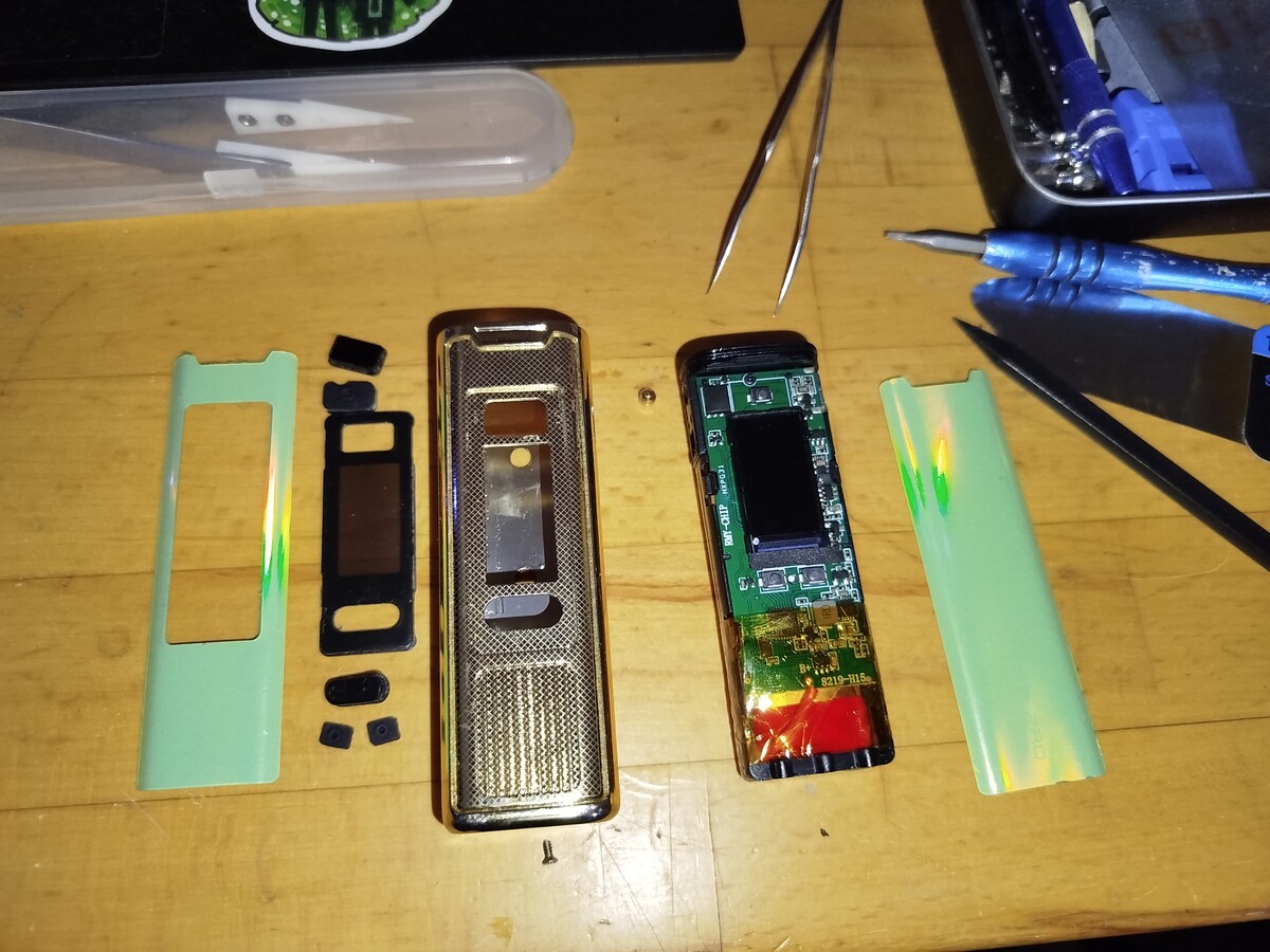
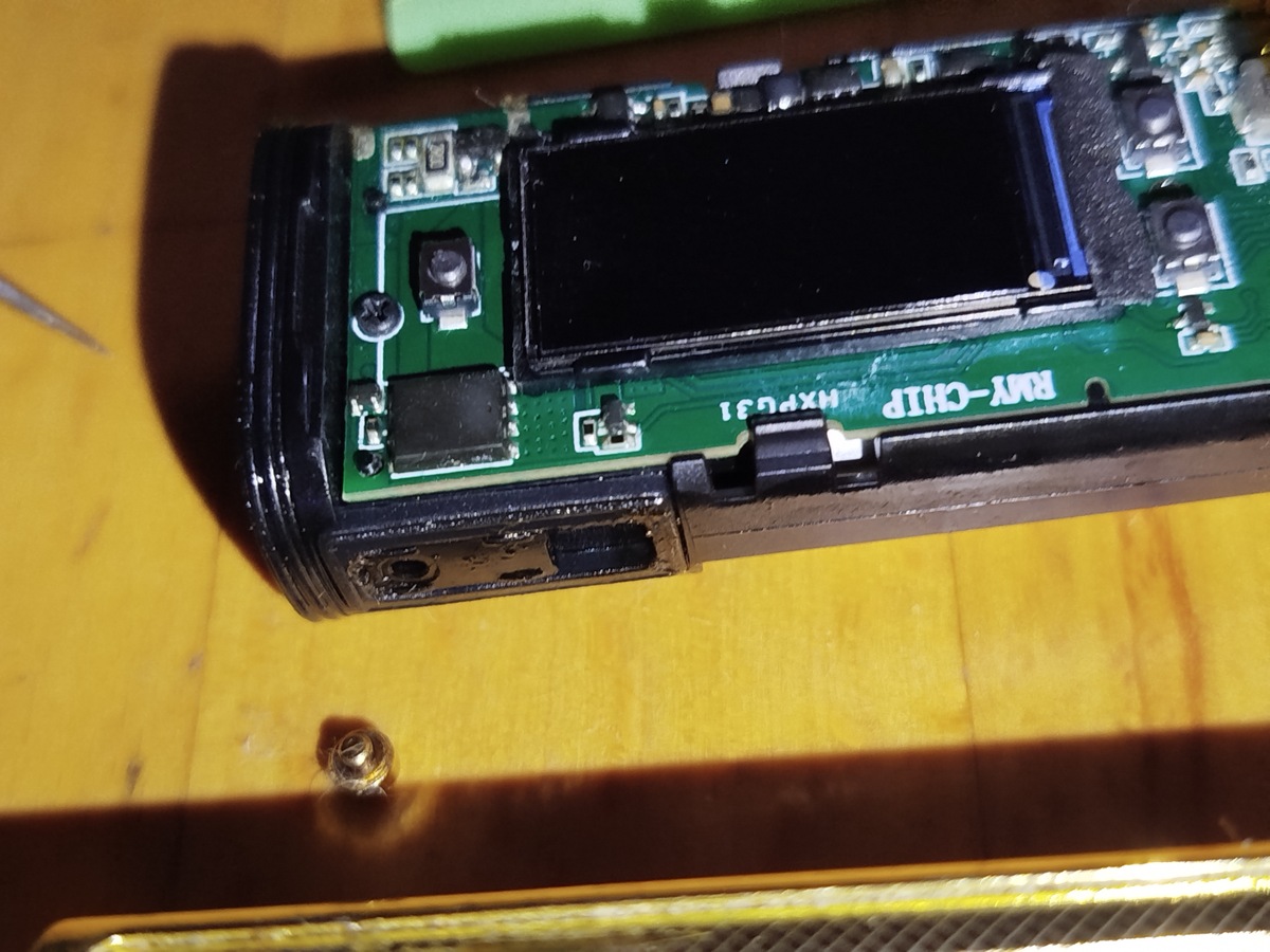
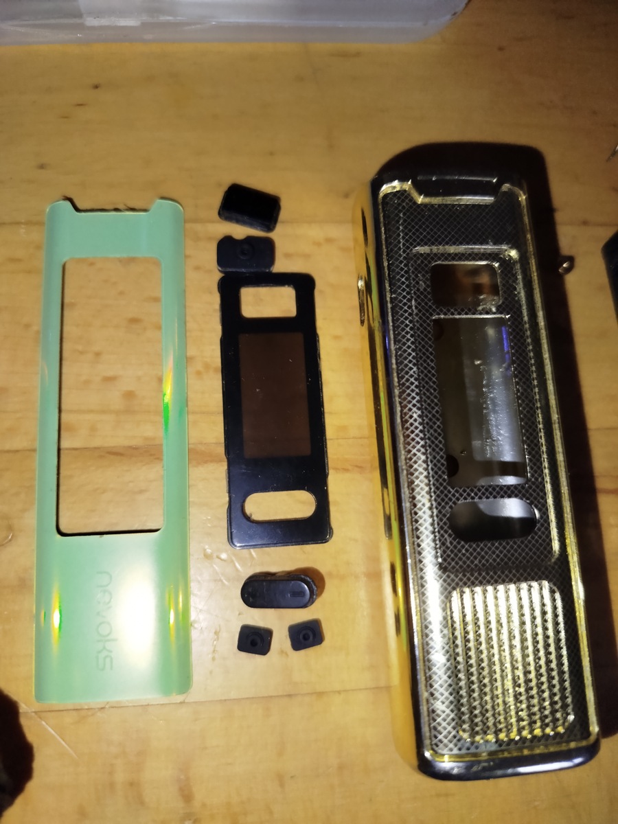
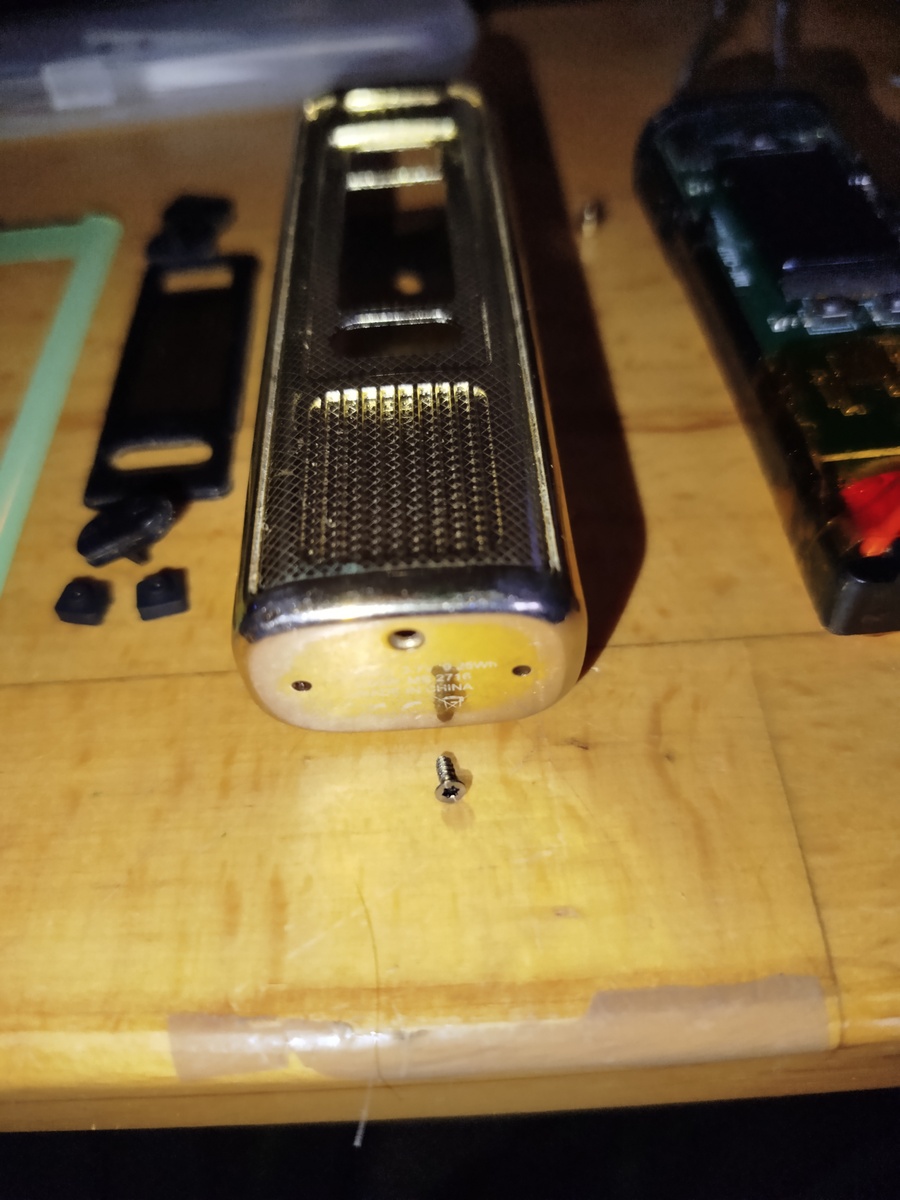
1 |
void display_init(void) {
|
2 |
|
3 |
// === 1. HARDWARE RESET ===
|
4 |
// Basis: DAT_40040000 = 0x40040000 (GPIO-Port-Basisadresse)
|
5 |
// Bit 3 (0x08) = RESET-Pin
|
6 |
|
7 |
GPIO[0x07] |= 0x08; // RESET → HIGH
|
8 |
delay_ms(1); // FUN_00004df8(1)
|
9 |
GPIO[0x07] &= 0xF7; // RESET → LOW (AND mit ~0x08)
|
10 |
delay_ms(1); // FUN_00004df8(1)
|
11 |
GPIO[0x07] |= 0x08; // RESET → HIGH
|
12 |
delay_ms_with_check(10); // FUN_00004e34(10)
|
13 |
|
14 |
// Zusätzlich: CS-Pin setzen (DAT_40040001, Bit 5 cleared via AND 0xDF)
|
15 |
GPIO[0x01] &= 0xDF; // CS → LOW (Chip Select aktiv)
|
16 |
|
17 |
// === 2. REGISTER UNLOCK (GC9A01-spezifisch) ===
|
18 |
spi_write_byte(CMD, 0xFE); // Inter-register command unlock 1
|
19 |
spi_write_byte(CMD, 0xEF); // Inter-register command unlock 2
|
20 |
|
21 |
// === 3. DISPLAY KONFIGURATION ===
|
22 |
spi_write_byte(CMD, 0xB0);
|
23 |
spi_write_byte(DATA, 0xC0); // Interface mode
|
24 |
|
25 |
spi_write_byte(CMD, 0xB2); // FRMCTR2 - Frame rate normal mode
|
26 |
spi_write_byte(DATA, 0x24);
|
27 |
|
28 |
spi_write_byte(CMD, 0xB3); // FRMCTR3 - Frame rate partial mode
|
29 |
spi_write_byte(DATA, 0x03);
|
30 |
|
31 |
spi_write_byte(CMD, 0xB7); // ETMOD - Entry mode
|
32 |
spi_write_byte(DATA, 0x01);
|
33 |
|
34 |
spi_write_byte(CMD, 0xB6); // DISSET5 - Display function control
|
35 |
spi_write_byte(DATA, 0x19);
|
36 |
|
37 |
spi_write_byte(CMD, 0xAC);
|
38 |
spi_write_byte(DATA, 0xDB);
|
39 |
|
40 |
spi_write_byte(CMD, 0xAB);
|
41 |
spi_write_byte(DATA, 0x0F);
|
42 |
|
43 |
spi_write_byte(CMD, 0x3A); // COLMOD - Pixel format
|
44 |
spi_write_byte(DATA, 0x05); // 16-bit RGB565
|
45 |
|
46 |
spi_write_byte(CMD, 0xB4); // INVCTR - Display inversion control
|
47 |
spi_write_byte(DATA, 0x04);
|
48 |
|
49 |
spi_write_byte(CMD, 0xA8);
|
50 |
spi_write_byte(DATA, 0x0C);
|
51 |
|
52 |
spi_write_byte(CMD, 0xB8); // Power control sequence
|
53 |
spi_write_byte(DATA, 0x08);
|
54 |
|
55 |
spi_write_byte(CMD, 0xED);
|
56 |
spi_write_byte(DATA, 0x03);
|
57 |
|
58 |
spi_write_byte(CMD, 0xEA);
|
59 |
spi_write_byte(DATA, 0x9F);
|
60 |
|
61 |
spi_write_byte(CMD, 0xC6); // FRCTRL2
|
62 |
spi_write_byte(DATA, 0x2A);
|
63 |
|
64 |
spi_write_byte(CMD, 0xC7);
|
65 |
spi_write_byte(DATA, 0x10);
|
66 |
|
67 |
// === 4. GAMMA POSITIV (0xF0) — 13 Bytes ===
|
68 |
spi_write_byte(CMD, 0xF0);
|
69 |
spi_write_byte(DATA, 0x09);
|
70 |
spi_write_byte(DATA, 0x35);
|
71 |
spi_write_byte(DATA, 0x2A);
|
72 |
spi_write_byte(DATA, 0x4A);
|
73 |
spi_write_byte(DATA, 0xA9);
|
74 |
spi_write_byte(DATA, 0x39);
|
75 |
spi_write_byte(DATA, 0x35);
|
76 |
spi_write_byte(DATA, 0x60);
|
77 |
spi_write_byte(DATA, 0x00); // ← Sonderfall: mov r0,r1 bei 0x364A
|
78 |
spi_write_byte(DATA, 0x14);
|
79 |
spi_write_byte(DATA, 0x0A);
|
80 |
spi_write_byte(DATA, 0x16);
|
81 |
spi_write_byte(DATA, 0x10);
|
82 |
spi_write_byte(DATA, 0x1F);
|
83 |
|
84 |
// === 5. GAMMA NEGATIV (0xF1) — 14 Bytes ===
|
85 |
spi_write_byte(CMD, 0xF1);
|
86 |
spi_write_byte(DATA, 0x13);
|
87 |
spi_write_byte(DATA, 0x24);
|
88 |
spi_write_byte(DATA, 0x55);
|
89 |
spi_write_byte(DATA, 0x3C);
|
90 |
spi_write_byte(DATA, 0xC6);
|
91 |
spi_write_byte(DATA, 0x16);
|
92 |
spi_write_byte(DATA, 0x3F);
|
93 |
spi_write_byte(DATA, 0x60);
|
94 |
spi_write_byte(DATA, 0x08);
|
95 |
spi_write_byte(DATA, 0x06);
|
96 |
spi_write_byte(DATA, 0x0D);
|
97 |
spi_write_byte(DATA, 0x1F);
|
98 |
spi_write_byte(DATA, 0x1C);
|
99 |
spi_write_byte(DATA, 0x10);
|
100 |
|
101 |
// === 6. SLEEP OUT + DISPLAY ON ===
|
102 |
spi_write_byte(CMD, 0x11); // SLPOUT - Exit sleep mode
|
103 |
delay_ms_with_check(100); // Pflicht-Delay nach SLPOUT (r0=0x64)
|
104 |
|
105 |
spi_write_byte(CMD, 0x29); // DISPON - Display on
|
106 |
delay_ms_with_check(10);
|
107 |
|
108 |
// === 7. BACKLIGHT EINSCHALTEN ===
|
109 |
GPIO[0x01] |= 0x20; // BL-Pin → HIGH (Bit 5 setzen)
|
110 |
set_pwm_backlight(0); // FUN_00005666(0) → PWM init mit Standardhelligkeit
|
111 |
}
|

 IMG_20260311_160002.jpg
(230 KB)
IMG_20260311_160002.jpg
(230 KB)
 IMG_20260311_160030.jpg
(240 KB)
IMG_20260311_160030.jpg
(240 KB)
 IMG_20260311_160045.jpg
(220 KB)
IMG_20260311_160045.jpg
(220 KB)
 IMG_20260311_160050.jpg
(230 KB)
IMG_20260311_160050.jpg
(230 KB)
 IMG_20260311_160137.jpg
(230 KB)
IMG_20260311_160137.jpg
(230 KB)
 IMG_20260311_160155.jpg
(220 KB)
IMG_20260311_160155.jpg
(220 KB)
 IMG_20260312_090823.jpg
(200 KB)
IMG_20260312_090823.jpg
(200 KB)