-
Thread
Raspberry Pi CM0 bei AliExpress, STMicroelectronics mit PX5, neue Messtechnik und AI-Assistenten
Blick auf die Performance von Linux 7.1 ermöglichen. ### Teledyne Caiman: Kameramodul für Ultra-Low-Light-Anwendungen. Wer in einem System in extremer Dunkelheit gut sehen muss bzw. möchte, könnte das neueste Kamera-Modul aus dem Hause Teledyne interessant finden. Es bietet eine Auflösung von 1,3
Typical burden voltage during range switching: 20 mV Range Switching Speed Upward switching (to higher current): • <2.5 µs to fully open the ranging MOSFETs @3.3 V Downward switching: • Min. ~380 µs, Max ~800 µs to fully open the ranging MOSFETs • Defaults to mA range at power-up
-
Thread
Power Profiling mit Saleae Logic Pro
DFG-Förderung beantragen. Da muss aber trotzdem noch mindestens ein Shunt dran und ob das Teil wirklich High Side messen kann? Ich glaube, für meinen Zweck wird das nicht das Richtige sein. Aber trotzdem danke.
weniger. Bei 1.8V Versorgungsspannung ist nicht viel Luft. Konkret benötige ich das gerade für ein Low Power RF SoC. Vor allem möchte ich die Länge bestimmter Betriebszustände beobachten, besonders Wake Up, Hochfahren des HF Teils, PLL Kalibrierung usw. Das lässt sich ganz gut am Stromverbrauch sehen
-
Thread
Klimaanlage steuern in Abhängigkeit von PV-Leistung
Gesamtlänge austesten. Anschließend die Zeitdifferenzen ausdrucken und nach Startbitlänge, Pausen, High/Low-bits suchen. Dann mit bitwrite abspeichern. Zuletzt durch Änderungen der Temperatur die Bitpositionen suchen. Meist ist das binär codiert also 1, 2, 4, 8. Steht alles in meinem Code. Bei der Checksumme
-
Thread
Sichere Ethernet-MCU, AI am Raspberry Pi, Lesestoff und mehr
0.5mm chip size as the 1st Generation product while adopting an internal structure that enables higher output. As a result, output power has been increased to approximately 4 times that of the 1st Generation product, reaching a maximum of 40µW. The higher output power improves the detectability of THz
detection. ROHM will also continue sales of 1st Generation devices for applications that prioritize low power consumption. For further information, please contact a sales representative or visit url=https://www.rohm.com/contactus]the contact page[/url] on ROHM’s website. Purchase of the evaluation kit
-
Artikel
Relais mit Logik ansteuern
Umschalten auch mit Hilfe eines D-FlipFlops realisieren. Funktion: Im Ruhemodus liegt der Ausgang Q auf LOW, Q negiert auf High Wird auf den Takteingang von IC1A eine steigende Flanke gelegt, wird der Highpegel vom Eingang übernommen, Q ist High, der MOSFET steuert durch und läßt das Relais anziehen, Q negiert ist Low. Bei der nächsten positiven Taktflanke wird der Pegel des negierten Ausgangs wieder übernommen, jetzt Low, und der Ausgang wird wieder auf Low geschaltet. Wird ein Taster verwendet muss dieser unbedingt
-
Thread
Identifikation Modbus-Controller-IC auf Platine
Sinn ergeben würde es, wenn der _SWIM_-Pin sowohl mit _nRE_ als auch _DE_ verbunden wäre: Ist _SWIM_ high, werden Daten empfangen, ist _SWIM_ low, werden Daten gesendet. Warum? Die einzige Alternative wäre _NRST_, und das ist einer der Standardpins des Controllers, der als Reset-Eingang verwendet wird.
-
Thread
STM32L073RZ läuft auf HSE nur halb so schnell wie erwartet
blinken: [c] void setup() { pinMode(PA5, OUTPUT); } void loop() { digitalWrite(PA5, LOW); delay(500); digitalWrite(PA5, HIGH); delay(500); } [/c] Funktioniert bis dahin. Die Blink-Frequenz der LED bestätigt, dass das Setup korrekt funktioniert. Dann habe ich mir
-
Thread
Alte Eproms sichern, welches Gerät?
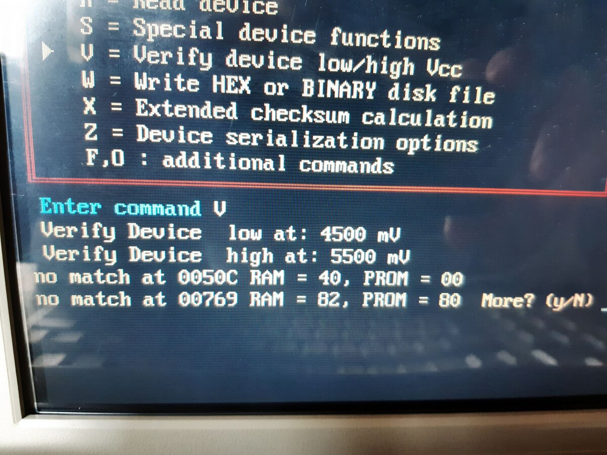
Meist liefert die höhere Spannung den richtigen Inhalt. Beim Beispiel im Anhang weicht der Verify high vom Verify nominal und Verify low ab. Da EPROMs der 27(C)xxx-Familie nach 0xFF löschen, ist das Image mit den meisten Nullen das richtige. 87(C)xxx löschen nach 0x00, da ist es umgekehrt.
-
Thread
EmbeddedWorld 2026, Catch-All – Bauteile, Stromversorgungen, Meshnetze uvam
zwei neue Controller nach folgendem Schema: [c] · Our New 32-bit MCU Lineup: Featuring the high-performance A34G34A (Cortex-M4F, 200MHz, 2MB Dual Bank) and the A31C144 entry-level series. The G43A demo showcases high-quality graphic LCDs powered by the LVGL library for modern appliance UIs. [
ins Rennen: [c] With the Proteus-IV and Ophelia-IV components, Würth Elektronik presents two new high-performance RF modules based on the latest Nordic nRF54L15-SoC semiconductor. The two modules differ only in terms of their firmware: Proteus-IV is a ready-to-use Bluetooth low-energy 6.0 module with
-
Thread
STM32I0 zum laufen (flashen) bringen (VSCode und PlatformIO)
mode : Software reset 21:39:52 : Device ID : 0x417 21:39:52 : Revision ID : Rev X 21:39:52 : Debug in Low Power mode is not supported for this device. 21:39:52 : UPLOADING OPTION BYTES DATA ... 21:39:52 : Bank : 0x00 21:39:52 : Address : 0x4002201c 21:39:52 : Size : 104 Bytes 21:39:52 : Bank : 0x01 21:39
haben einen Debug-UART integriert, und sie sind deutlich schneller, weil stärkerer Prozessor und High-Speed USB statt Full-Speed USB. https://www.reichelt.de/de/de/shop/produkt/in-circuit-debugger_-programmierer_fuer_stm32_usb-c-330303 fchk
-
Thread
[V] Spectro-Color Platinen CV12864B LCD Display Ersatzteile
genauer angesehen: Der Analog Frontend für den Sensor ist ein AD7888 (12-Bit ADC), dazu zwei AD822 (Low Power FET-Input Op Amp). Die Versorgungsspannung über die Buchse beträgt vermutlich 6 Volt (das ist die Mindestspannung, wie viel maximal erlaubt ist habe ich nicht ausprobiert), der Stift ist dabei
beiden anderen 2-Pin Stecker ist unklar, am Größeren der beiden liegen die Ausgänge des TC4427 (DUAL HIGH-SPEED, POWER MOSFET DRIVERS). Die Stiftleiste am Batteriefach ist für BDM des HC12, Belegung siehe Bild. Eine Firmware ist bei meiner Platine nicht im Flash, allerdings befindet sich eine Firmware
-
Thread
Frage zur Beschaltung eines PIC12F1840 zur Abfrage von Widerstandswerten
der Taster und des Potis > programmtechnisch realisiert? Man könnte den Pin kurz auf Ausgang und High schalten, dass der 10nF Kondensator geladen wird. Und dann den Pin auf Eingang umschalten und messen wie lange er braucht, um Low zu werden. So ähnlich wurden ganz ohne ADC z.B. die Joysticks am
-
Thread
Ladezustand Elektroauto (Typ2 Ladung)
relevante Kommunikation passiert über den CP Pin im Ladestecker. Dabei gibt es zwei Mechanismen. Low-Level Kommunikation: Die Ladesäule signalisiert über den Dutycycle eines PWM-Signals den maximal möglichen Ladestrom bzw. die Verwendung der Highlevel-Kommunikation. Das Fahrzeug ändert durch das Zuschalten eines Widerstands den Spannungspegel am CP Pin und signalisiert so seine Ladebereitschaft. High-Level Kommunikation: Ethernetpakete werden per Powerlinekommunikation auf den CP Pin zusätzlich aufmoduliert. Auch moderne AC-Wallboxen können damit gemäß ISO 15118 den Ladezustand des Fahrzeugs auslesen
-
Thread
Quelloffene Spracherkennung, LoRA am Raspberry Pi, neue Jetson-Module uvam
tracking, and overall preference. In terms of hit score, the gamers’ win rate improved by 38% at the highest level of 480Hz compared to the lowest level of 60Hz. Despite significant gains being achieved even at 240Hz, the win rate increased by an additional 10% at 480Hz. This indicates that gaming performance
-
Thread
Merten KNX-Netzteil 683829 - defekt
nicht ganz sicher ... wegen dem Aufdruck "5l" ?!? EE-A 47U 400B -- Elko radial, 47µF, 400V, 105°C,high ripple VF 100/16 P-D -- Elko SMD, 100µF, 16V, 2000h, low ESR
-
Thread
Neue Bauteile – kleine Relais, nicht durchbrennende LED-Serienschaltungen und Co
2.5mm) size. This product delivers highly efficient power conversion and stable performance under high-voltage conditions, making it suitable for onboard chargers (OBCs) in electric vehicles (EVs) and power supply circuits in high-performance consumer devices. [/c] ### Tektronix-Museum: Jahreskalender
den sonstigen RF-Eigenschaften vermeldet folgendes: [c] THE BIG DEAL y Wideband, DC to 30 GHz y Low Insertion Loss, Typ. 1.8 dB y High Isolation, Typ. 47 dB y High Input IP3, Typ. +46 dBm y Fast Rise/Fall Time, Typ. 23.1 ns/6.4 ns y 4x4 mm, 24-Lead QFN-Style Package [/c] ### Renesas - Gen6
-
Artikel
Fehlersuche
Schaltung an? Liegen die richtigen Signale an den Zwischenpunkten der Schaltung an? Sind Logikpegel sauber LOW und HIGH? Wenn nein, dann sind oft mehrere Ausgänge gleichzeitig auf einem Bus aktiv und ziehen in verschiedene Richtungen (Low und High). Oder Die Ausgänge sind zu schwach, um die Lasten zu treiben
um Zeitverhalten von Software zu messen, z.B. Interruptroutinen. Zum Beginn setzt man ein Pin auf HIGH, am Ende auf LOW, das kann man dann sehr einfach mit einem Oszilloskop messen Ebenfalls kann man mit so einem Testpin den Anfang eines speziellen Programmablaufs signalisieren, um ein Oszilloskop zu
-
 Bild
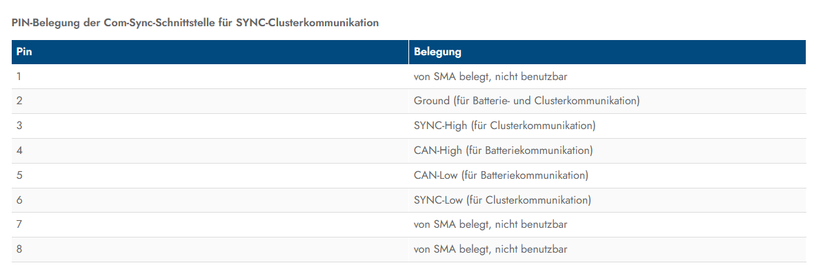
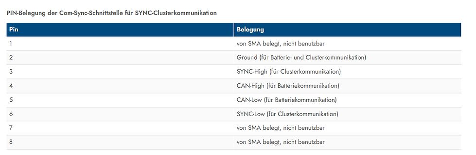
Tabelle der Pin-Belegung einer Com-Sync-Schnittstelle
1 | von SMA belegt, nicht benutzbar 2 | Ground (für Batterie- und Clusterkommunikation) 3 | SYNC-High (für Clusterkommunikation) 4 | CAN-High (für Batteriekommunikation) 5 | CAN-Low (für Batteriekommunikation) 6 | SYNC-Low (für Clusterkommunikation) 7 | von SMA belegt, nicht benutzbar 8 | von SMA belegt
-
Thread
FPGA verrechnet sich sporadisch
agiert. Auch der Kompressor springt bei 70% teilweise verfrüht an. Es wird also irgendwann ein Bit high, obwohl es noch low sein müsste. Ich nehme an, daß es ein Bit im Bereich (21 .. 20) ist, daß unzulässig mit aufaddiert wird. Leider kann ich es nicht testen, weil ich keinen debug core dort einsetzen
-
 Bild
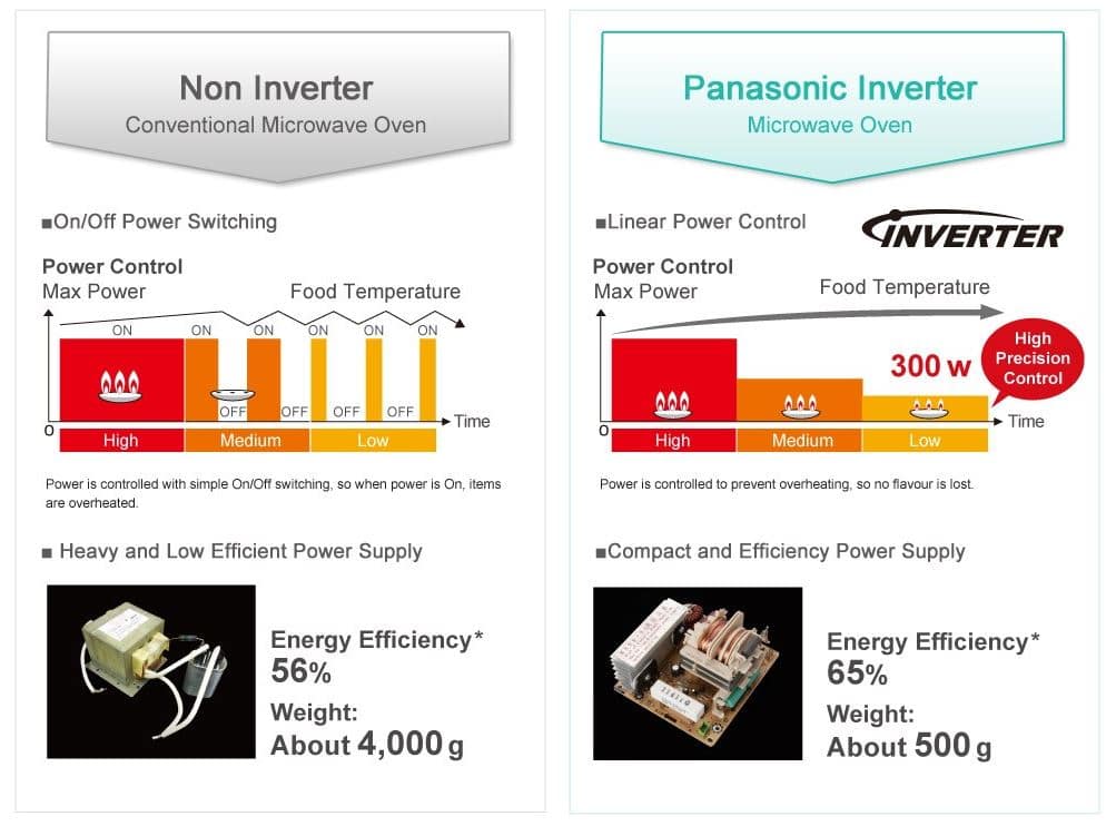
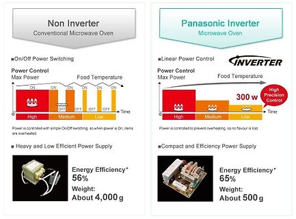
Vergleich Non-Inverter und Panasonic Inverter Mikrowellen-Technologie
Microwave Oven On/Off Power Switching Power Control Max Power Food Temperature ON ON ON OFF OFF OFF High Medium Low Time Heavy and Low Efficient Power Supply Energy Efficiency* 56% Weight: About 4,000 g Panasonic Inverter Microwave Oven Linear Power Control Power Control Max Power Food Temperature High
-
 Bild
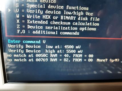
Textmenü eines Programms zur Geräteprüfung
S = Special device functions V = Verify device low/high Vcc W = Write HEX or BINARY disk file X = Extended checksum calculation Z = Device serialization options F,O : additional commands Enter command V Verify Device low at: 4500 mV Verify Device high
-
 Bild
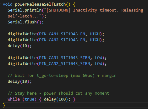
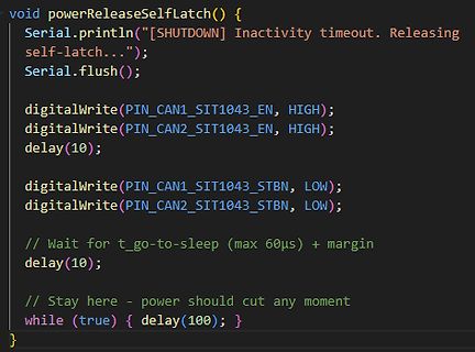
C++ Code für eine Shutdown-Funktion
Inactivity timeout. Releasing self-latch..."); Serial.flush(); digitalWrite(PIN_CAN1_SIT1043_EN, HIGH); digitalWrite(PIN_CAN2_SIT1043_EN, HIGH); delay(10); digitalWrite(PIN_CAN1_SIT1043_STBN, LOW); digitalWrite(PIN_CAN2_SIT1043_STBN, LOW); // Wait for t_go-to-sleep (max 60µs) + margin delay(10);
-
 Bild
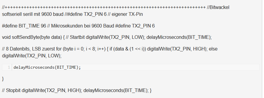
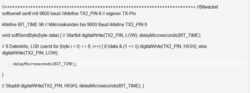
C++ Programmcode für Software-Serielle Schnittstelle
bei 9600 Baud #define TX2_PIN 6 void softSendByte(byte data) { // Startbit digitalWrite(TX2_PIN, LOW); delayMicroseconds(BIT_TIME); // 8 Datenbits, LSB zuerst for (byte i = 0; i < 8; i++) { if (data & (1 << i)) digitalWrite(TX2_PIN, HIGH); else digitalWrite(TX2_PIN, LOW); 1 delayMicroseconds(BIT_TIME); } // Stopbit digitalWrite(TX2_PIN, HIGH); delayMicroseconds(BIT_TIME); }
-
Artikel
Fahrroboter
Motoren werden über ein digitales Signal gesteuert (orangene Ader). Das Signal besteht aus einer High-Pegel-Phase und einer Low-Pegel-Phase. Die Dauer der High-Pegel-Phase bestimmt die Zielposition (1ms = Gegen den Uhrzeigersinn bis zum Anschlag; 2ms = Im Uhrzeigersinn bis zum Anschlag). Da weder Anschlag
gesteuert werden (1000µs = Vollgas gegen den Uhrzeigersinn; 1600µs = Langsam im Uhrzeigersinn). Auf die High-Pegel-Phase folgt eine Low-Pegel-Phase von mindestens 3ms. Die eingebauten Motoren sind sehr stark und bremsen den Roboter bei einem kurzen Impuls gegen die Laufrichtung auf der Stelle ab. Dabei erhöht
-
 Bild
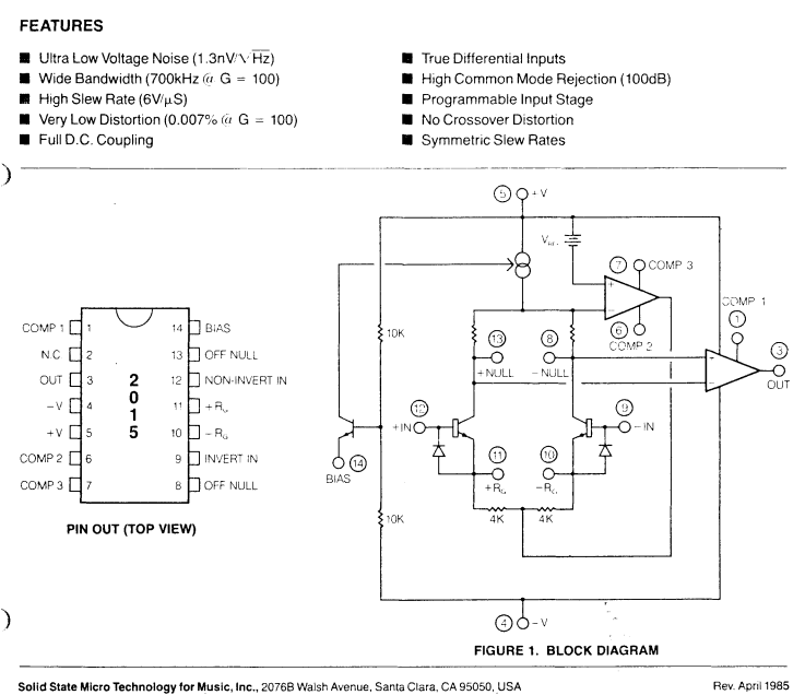
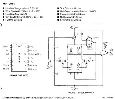
Datenblatt-Ausschnitt mit Pinout und Blockschaltbild eines Operationsverstärkers
FEATURES Ultra Low Voltage Noise (1.3nV/V Hz) Wide Bandwidth (700kHz (@ G = 100) High Slew Rate (6V/µS) Very Low Distortion (0.007% (@ G = 100) Full D.C. Coupling True Differential Inputs High Common Mode Rejection (100dB
-
 Bild
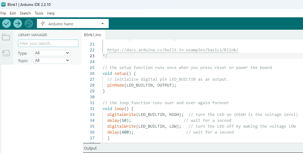
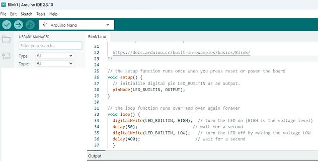
Arduino IDE Code für Blink-Beispiel
the loop function runs over and over again forever 31 void loop() { 32 digitalWrite(LED_BUILTIN, HIGH); // turn the LED on (HIGH is the voltage level) 33 delay(50); 34 digitalWrite(LED_BUILTIN, LOW); // turn the LED off by making the voltage LOW 35 delay(400); 36 } 37 Output
-
 Bild
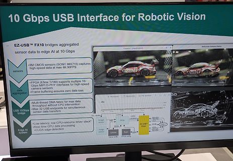
Präsentation einer 10 Gbps USB Schnittstelle für Robotic Vision
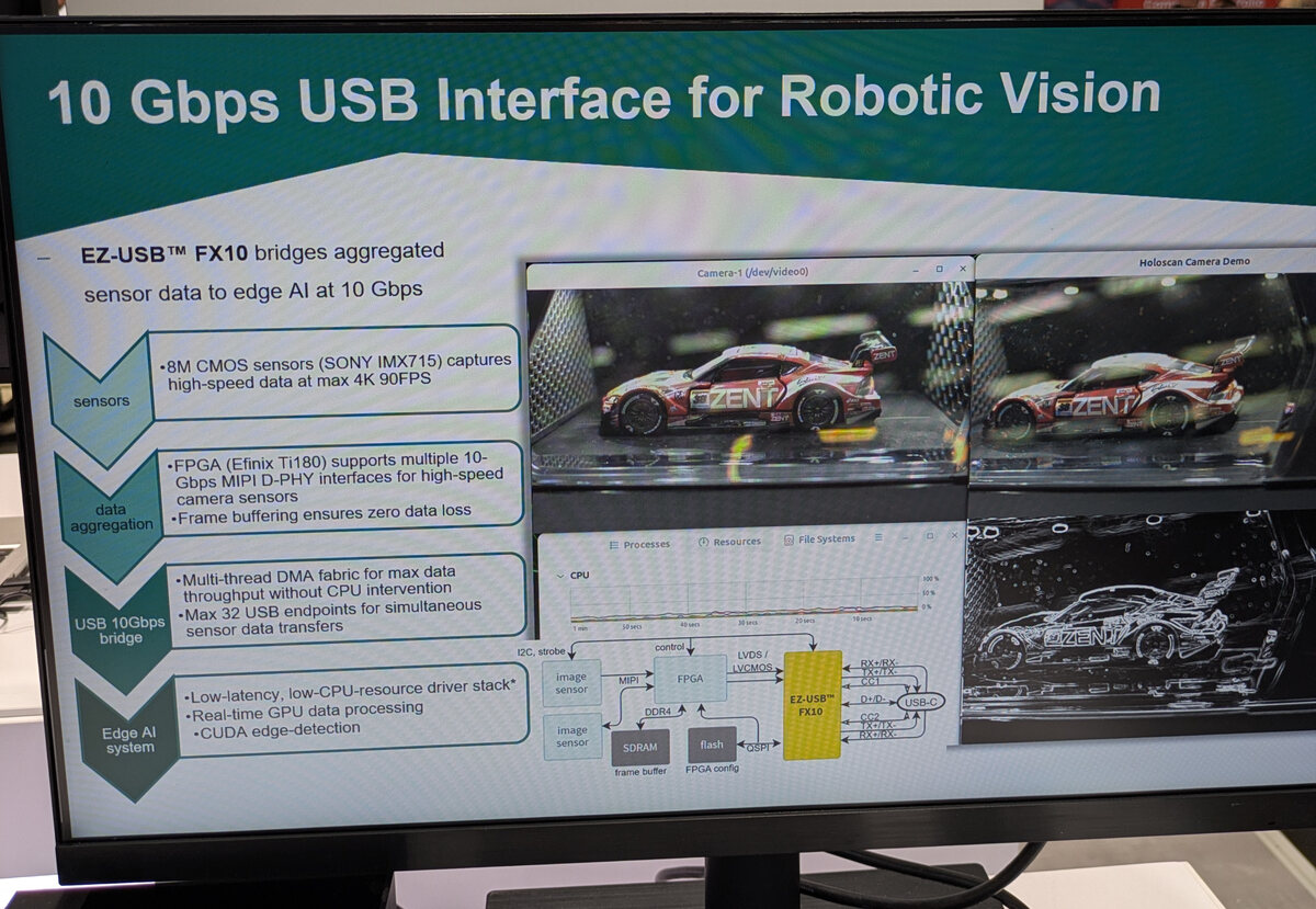
FX10 bridges aggregated sensor data to Edge AI at 10 Gbps 8M CMOS sensors (SONY IMX715) captures high-speed data at max 4K 90FPS FPGA (Efinix Ti180) supports multiple 10-Gbps MIPI D-PHY interfaces for high-speed camera sensors Frame buffering ensures zero data loss Multi-thread DMA fabric for max data throughput without CPU intervention Max 32 USB endpoints for simultaneous sensor data transfers Low-latency, low-CPU-resource driver stack Real-time GPU data processing CUDA edge-detection image sensor image sensor FPGA SDRAM flash frame buffer FPGA config I2C, strobe control LVDS / LVCMOS EZ-USB™
-
 Bild
Features eines Beschleunigungssensors
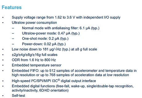
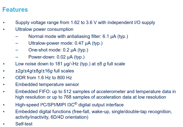
- Ultralow-power mode: 0.47 µA (typ.) - One-shot mode: 0.2 µA (typ.) - Power-down: 0.02 µA (typ.) Low noise down to 181 µg/√Hz (typ.) at ±8 g full scale ±2g/±4g/±8g/±16g full scales ODR from 1.6 Hz to 800 Hz Embedded temperature sensor Embedded FIFO: up to 512 samples of accelerometer and temperature data in high resolution or up to 768 samples of acceleration data at low resolution High-speed I2C/SPI/MIPI I3C® digital output interface Embedded digital functions (free-fall, wake-up, single/double-tap recognition