d-c-fix Klebefolien sind mir eher in unguter Erinnerung.
Hat schon mal jemand eine Türe mit d-c-fix beklebt, taugt das was? > Diese d-c-fix Klebefolien sind mir eher in unguter Erinnerung. Niemand tut so etwas? Was macht deine Zarge? Scharnier und Zarge passen nicht zueinander.
1MB. Da gab es auch Grafikkarten für CAD (Stichwort Weitek), schweineteuer, mehrere tausend DM. TIGA ist auch so ein vergessener Versuch: https://www.vogons.org/viewtopic.php?t=79599
gesehen. Oder gilt inzwischen 10 Ocken als Mondpreis heute ... Zu der habe ich noch zwei originale c't BIOSse. 1988/1989 als c't noch tief in der Hardware mitgemischt hat, konnte man entweder komplette BIOS-Chips bei heise bestellen, oder auch nur das File zum Flashen herunterladen. Zugriff auf die
sich laut Firmenangaben noch nach Jahren löten Eildienst 2h: Versand am selben Tag bei Einsendung bis 13:00 400€ für 2dm² B&B Sachsenelektronik GmbH. Homepage: Klein- und Musterserien, Spezialist Sondertechniken Zusätzliche Partner für Großserien in Asien mit eigenen Mitarbeitern Ein- und Doppelseitige
Leiter) 41,44 ? PCB Pool 50,27 100,54 Q-print/Q-PCB 55,62 95,89 mit Lötstopp, mit E-Test AISLER 31,13 31,13 Fischer Leiterplatten GmbH (10AT) 46,41 73,07 LEITON 88,79 147,39 Multi PCB Ltd. Leiterplatten (6AT) 78,06 156,13 M & V Leiterplatten - Vertriebs GmbH 62,83 125,66 Onlineshop WEdirekt 128,75 172,38
beurteilen. Es gibt Liebhaber, die fahren ihre bestens erhaltenen E34 nur bei Trockenheit und mehr als 15 °C, die wissen vielleicht um das Problem, das tritt bei diesen Fahrzeugen aber nicht auf, weil der Scheibenwischer quasi nie benutzt wird. Andere fahren die Autos herunter, denen ist das weitestgehend
auf Lager halten, teurer. Und dann erinnert euch mal an eure traurige Jugend, da waren Autos nach 13-14Jahre so verrostet das sie alle entsorgt wurden. Autos halten heute laenger wie frueher. Sind also besser geworden, haben mehr Funktionen und verbrauchen weniger Benzin, dabei fahren die Leute mehr
on a single low power FPGA. [/c] Interessant ist in der Pressemeldung auch die folgende Passage, die auf eine AI-Anwendung im Weltraum eingeht: [c] , Spacecraft Pose Network v2 (SPNv2), a neural network designed to estimate
2026 im Zeichen der “All Electric Society” Für die dieses Jahr vom 10. bis zum 13. November stattfindende Ausgabe der electronica wurde die Parole der “All Electric Society” ausgegeben: [c] The electronics industry provides the technological basis for the All Electric Society and
, ein LiFePo4 Akku, der draußen steht, muß beheizt werden, sonst ist das sinnlos. Unterhalb von 10°C Zellentemperatur muß der Ladestrom signifikant reduziert werden, bis auf Null bei ca. 0°C. Oliver
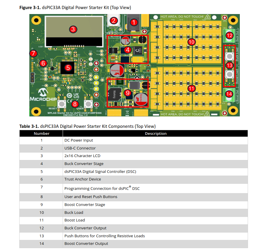
Programming Connection for dsPIC DSC User and Reset Push Buttons MPLAB Starter Kit for dsPIC33A912MPS506 DM30017-4 Rev 1.0 Table 3-1. dsPIC33A Digital Power Starter Kit Components (Top View) Number Description 1 DC Power Input 2 USB-C Connector 3 2x16 Character LCD 4 Buck Converter Stage 5 dsPIC33A Digital
Elektronikingenieure aus Russland haben es nachgebaut. Das ist mein Bauprojekt. https://www.youtube.com/watch?v=DM-f5JLvSmU
alten" Gerät grade recht. Oder wie sagte mein Freund, als ich ihm aufgezählt habe, was an meinem 13 Jahre alten Auto alles nicht funktioniert: "Sag doch gleich, dass du ein Neues willst!"
internal clocks again provide a transition. reset signal for the start F/F. www.national.com 18 D C Functional Description (Continued) 0 0 / A C 0 8 2 A D C 8 3 A D C 8 0 / A C 0 0 5 DS005671-13 Note 13: CS shown twice for clarity. Note 14: SAR= Successive Approximation Register. FIGURE 4. Block Diagram
Kleinstaufträgen verdient man ja nicht viel. Bei AISLER habe ich einmal bestellt, da gab es zwar € 10 µC.net Rabatt aber dort hatte ich das Gefühl mit meinen drei Platinchen mehr Aufwand zu erzeugen als dabei rum kommt. Jörg W. schrieb im Beitrag #8069134: > Noch vor wenigen Jahren mussten wir selbst
ausländische Hersteller nicht ausreichend bestrafen. Also nicht wundern, wenn du dann statt 3€ eben 60DM pro Platinen-Lieferung an den Zoll zahlen musst. Make Deutschen Zoll Great Again!
V5.04 CYPRESS PLD CY7C371i(TQ44) ADP-7C371-Q No Need WA7C37X V5.04 CYPRESS PLD CY7C372 ADP-7C371 No Need WA7C37X V5.04 CYPRESS PLD CY7C372i ADP-7C371 No Need WA7C37X V5.04 CYPRESS PLD CY7C373 ADP-7C374-PL/Q No Need WA7C37X
8 8052A/ B 4 8068A 71C03A B 2 B 1 FIGURE 8. ICL8052A-8068A/71C03A PLASMA DISPLAY CIRCUIT 13 ICL8052A/ICL71C03, ICL8068A/ICL71C03 A suitable circuit for driving a plasma-type display is shown driver circuit could be ganged
7.7 - h 10 mm 200-340 Neosid 5049 , 7 1/4 turns BV- nH Q 75 ( @ 40 MHz @ 270 nH ) 5049 2,20 □ 7 - h 13 mm 5 turns , 58 pF capacity coil Q > 65 ( 25 ÷ 85 MHz ) 210 - 400 resonance L+C = 35-47 MHz BV- 1,50 nH if it will be used as resonant circuit the m2019 frequency will be about 45 MHz □ 7 - h 13 mm 5
C 2 1 0 7 32 T 2 C0 C 9 1 8 1 823 32 3 P 4 C 3C C T P C 013C 2 2 T 913 4 P 0 P C 2 T 2 T 71 41 P P 3C 3C 02 T T 3C 0 5 6 3 6 13 5 P 5 1 13 C 30 T P C C T 5 P 2 T P T 0 1 GRUNDIG Service Chassis G5 E 3
_1 R Tot_1 R Tot_1 R Tot_1 c Δx PSR 1 R Total1 X TotlX Sat_2 Y Tota Y Sat_2 Z Tota ZSat_2 c Δy R Tot_2 R Tot_2 R Tot_2 PSR 2 R Total_2 = (13a) Δz X TotaX Sat_3 Y Tota Y Sat_3 Z Tota
MOS-FET. Gate threshold voltage : VGS(th) min. 0.1V max. 2V On resistance : R DS(on) max. 100 Ohm @ I = DmA, V = 2GSV Input capacitance : C iss max. 100 pF @ V DS1V, V GS= 0V Switching times : ton off max. 50 ns. Allowed drain current : D 10 mA or higher. Values of pull-up resistors and series resistors are
. Da s emo-Signalal von CH ANNEL 1 1 (K ANAL 1)trennnen und a nhand derna chstehendenen Schrit ean C HANNEL EL 2 (KA NAL 2) anlegen. 1-13 Inbettri bnahme D rchführen von M sungen ngen CHANNEL1 Al C Damae Lvl: V OsMAX.502 CHAWJEL2 <θ√ Z ≡C≥k rh Ö: Damags Lvi: 5Vrms MAX.502 M/ Freq & MΓ Ď / Ratio E R
/IP Stack inklusive. Leicht zu erlernen und viele Beispiele NuttX RTOS (ARM7TDMI port for TI TMS320C5471 also called a C5471 or TMS320DM180). Phoenix-RTOS PicoOS Prex is a portable real-time operating system for embedded systems. The small, reliable, and low power kernel is written in the C language
STMicroelectronics The RX MCU Design Contest und die Top 3 im Video bei Dave Jones auf EEVBlog.com ARM Cortex-M3 PSoC® 5 Design Challenge SparkFun Microcontroller Contest bis 13.02.2011 EFM32 Design-Wettbewerb von Elektronik, Avnet-Memec und Energy Micro Make It Challenge: Kinetis MCUs von Freescale 2010 SchmartBoard
on outputs 4, 6 and 8 of IC 13. The reset flip-flop FF1 is triggered at the end of pulse at the output of gate C resets the gate period selected by switch SI. IC14 . . . IC16. A new gate period Depending upon the position of the commences
S 9 0 A 2 0 0 H TO5 C r " Oo > TO"S C5 TO0 3 c o 3 13 iS = T O 0 3 T O T O 'O TO ■ O U J 0 3o TO C = 5 f , 3 3S wNi ^D V ) TO E i ? C TO TO v>TO < T O 3 TO ^^TO ^TO TO | | w T O T O! r £: Oo TO2 " ? C TO ^ 2 ^ 5 ■T O C 3

 Bild
Bild
 Bild
Bild
 Bild
Bild