Universal-Netzteil, 36 Watt. Die Spannung kann man am Gerät auf 5 V oder 6 V oder 7,5 V oder 9 V oder 12 V oder 13,5 V oder 15 V stellen. Der maximale Strom ist immer 2,4 A. Das könnte helfen. MfG egonotto
Möglicherweise lässt sich auf Grundlage eines Bausteins wie des TPS25772 (https://www.ti.com/lit/ds/symlink/tps25772-q1.pdf) etwas derartiges konstruieren. Hierfür gibt es auch ein Evaluation Board, dessen Dokumentation weitere Aufschlüsse bieten sollte, ob der Chip, dessen Datenblatt und Beschreibung
- Verpolungsschutz? und sehe auch nicht wie sie > genau verdrahtet ist. https://www.ti.com/lit/ds/symlink/lm2596.pdf Schau ins verlinkte Datenblatt. Wenn die hin ist, fabriziert sie einen Kurzschluss vom Ausgang nach Masse. Am Feedback Pin ist bei den einstellbaren Ausführungen ein Spannungsteiler
dc-constant-voltage-and-constant-current-with-led-voltmeter-step-down-power-module/ Auch die aufgedruckte Bezeichnung BTE13-001 findet ein paar Fotos https://www.thingiverse.com/thing:5904541 sogar ein 3d-gedrucktes Gehäuse dazu
wodurch der Entwicklung U3 12 Zeitkondensatorkreis von der Startschaltung getrennt wird. –(11-9) – 13,5–14,5 T1 (11-9) – 12 13,5–14,5 – Der Kondensator entlädt sich über den im Stromstabilisatorkreis T2 angeschlossenen Transistor T29-U3. Die Entladerate des (10,5-11,5) – –(10,1–11,1) – (11,0–10,4) –
current I (5) 0.8 A OS(5) Maximum sink current IOSI 1 A Gate drive pull-up resistance R V = 1V 8 Ω UP DS HS gate drive pull-down resistance RHS-DN V DS= 1V 1.2 4.3 Ω LS gate drive pull-down RLS-DN V DS= 1V 1 5 Ω resistance LS passive pull-down R LS-PDN 590 kΩ resistance LS automatic turn-on time LS At ENx
choice of low-side FET is a trade-off between P = 1 –- - - I 2 r (EQ. 10) conduction losses (r DS(ON) ) and cost. A good rule of thumb for Q2 VIN BAT DSON the rDS(ON) of the low-side FET is 2x the DS(ON) of the high-side FET. Choose a low-side MOSFET that has the lowest possible on- The LGATE
target/rp2040.cfg [/code] lautet übrigens: [code] Open On-Chip Debugger 0.12.0+dev (2026-03-13-15:21) Licensed under GNU GPL v2 For bug reports, read http://openocd.org/doc/doxygen/bugs.html adapter speed: 250 kHz Warn : Transport "swd" was already selected Info : [rp2040.core0] Hardware
https://pip-assets.raspberrypi.com/categories/610-raspberry-pi-pico/documents/RP-008276-DS-1-getting-started-with-pico.pdf?disposition=inline (Seite 19) sagt: Pico A GND -> Pico B GND Pico A GP2 -> Pico B SWCLK Pico A GP3 -> Pico B SWDIO Wo hast Du Dein Wiring her? "-c "transport
für den TL431 weniger stark runtergeteilt, und der Ripple weiter reduziert, in der Simulation von 13 Volt am Eingang auf 0.12 mV am Ausgang, das sind 100 dB.
bipolaren Transistoren bleiben. Der IRF820 hat recht viel nichtlineare Kapazität vor allem wenn V_DS klein ist. Der ist auch obsolet, wäre also nicht meine erste Wahl. Wenn du C8/R8 verwendest dann ziehst du die Regelschleife stark an, dann braucht es auch C6 damit die Verstärkung von Q3 nicht zu
Current CC(ST) V CC= 13.5 V 2 − 3 −4.5 −2.5 −1.2 mA Startup Current Biasing V CC(BIAS) ICC−500µA 2 − 3 8.0 9.6 10.5 V Threshold Voltage Normal Operation Average Switching Frequency fOSC(AVG) 8 − 3 58 65 72 kHz Switching Frequency
supply board for the following circuit description. Alarm Sensing LED Indicators. LED indicators (DS2 through DS8 and DS13) are placed on the input voltage side of the Power Supply Supervisor, U9. These indicators provide a quick visual check to see if the expected input voltages to U9 are present if
Bekanntlich greifen unter Windows 9x/Me Portzugriffe ungehindert zur Hardware durch, außer die durch VxDs abgefangenen.) Dann macht avrdude die üblichen IN+OUT-Befehle. Jeder dieser Befehle generiert eine (IMHO) Allgemeine Schutzverletzung, also Int13 (General Protection Fault #GP). Bevor die sattsam bekannte
null , damit wird die unnütze Ausgabe des Befehls verborgen. Siehe auch: mysmartUSB V2.11 und ATtiny 13. mysmartUSB V2.11 verlangt -cavr910 als Programmer. Leider ist in avrdude 5.10 immer noch nicht der ATtiny13 damit zu programmieren. Also in die avrdude.conf folgendes mit unter ATtiny13 aufnehmen, so
primary controller on InnoSwitch3-EP is a Quasi-Resonant (QR) UNDER/OVER INPUT VOLTAGE (V) Pin (Pin 13) flyback controller that has the ability to operate in continuous A high-voltage pin connected to the AC or DC side of the input bridge conduction mode (CCM), boundary mode (CrM) and discontinuous for
Technologies 1990-1992, 1999. [/c] (Unter https://www.pcbway.com/project/shareproject/Dallas_DS1225Y_FRAM_Adapter_3c961bed.html gibt es außerdem einen FRAM-Adapter, der auf der Hauptplatine des 53310A funktioniert) ### electronica 2026 im Zeichen der “All Electric Society” Für die dieses Jahr vom 10. bis zum 13. November stattfindende Ausgabe der electronica wurde die Parole der “All Electric Society” ausgegeben: [c] The electronics industry provides the technological basis for the All Electric Society and
Your Company GND Sheet: 1/1 Date: 2019-05-14 Drawn By: g3gg0.de 1 2 3 4 5 1 2 3 4 5 A VCC A R4 2k2 U9 DS18B20U+T&R TEMP_INT 1DQ VDD 2NC NC 3NC NC 4GND NC B B C C D D TITLE: Sheet_1 REV: 1.0 Company: Your Company Sheet: 1/1 Date: 2019-08-04 Drawn By: g3gg0.de 1 2 3 4 5 1 2 3 4 5 A A B B VCC5 VCC E13 E1 UDD32C05L01
data are ignored, and not displayed on the LCD screen. -19 of 28 - T6963C Application Notes Issue: 2/13/94 10.1.3 Example RAM Map for single screen drive LCD 0000H Graphic Ram Area (0000H-13FFH: 5120 bytes) 13FFH 1400H Attribute RAM Area 16FFH 1700H Text RAM Area (1700H-1BFF: 1280 bytes) 1BFFH 1C00H CG-RAM
by Equation 28: peak current into the switches is around 400 mA and the TJ Tamb maximum allowable R DS(on)for the MOSFET is given by Pmax + (28) Equation 29: Rth j R DS(on)(max) + P (29) Under the above conditionsJ T = (150−60)/150 = 600 mW DRMS 2 2 This value yields a zero safety margin because it assumes
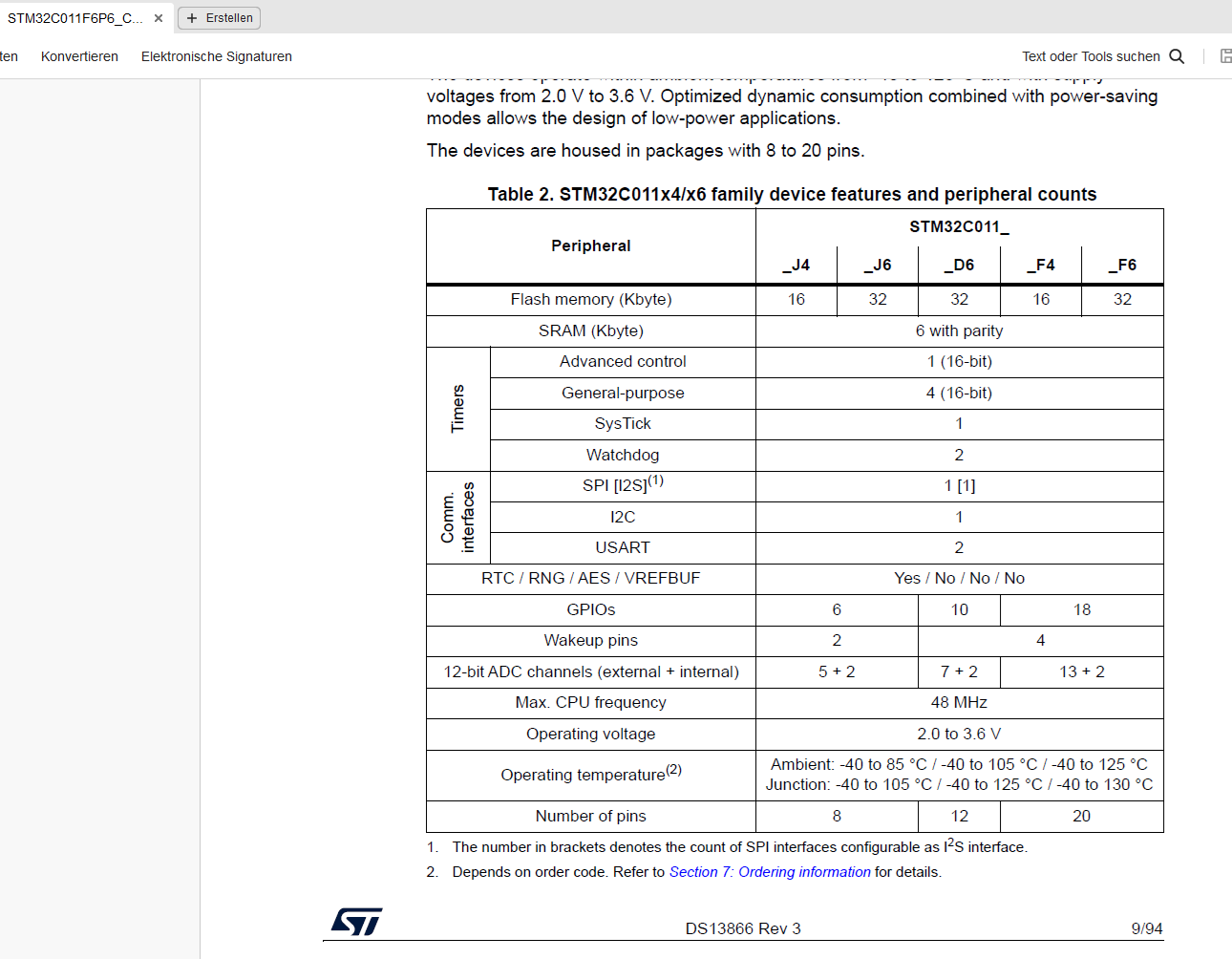
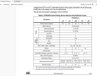
/ No / No / No
GPIOs 6 10 18
Wakeup pins 2 4
12-bit ADC channels (external + internal) 5 + 2 7 + 2 13 + 2
Max. CPU frequency 48 MHz
Operating voltage 2.0 to 3.6 V
Operating temperature (2) Ambient: -40 to 85 °C / -40 to 105 °C / -40 to 125 °C
Junction: -40 to 105 °C / -40 to 125 °C / -40 to 130 °C
Number of pins 8 12 20
ST DS13866 Rev 3 9/94
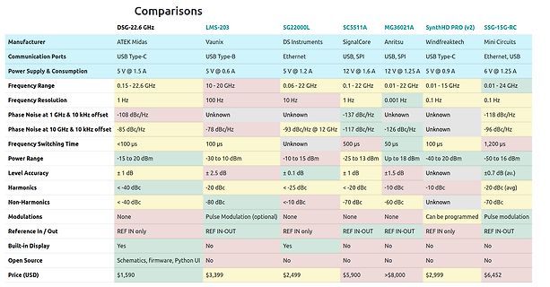
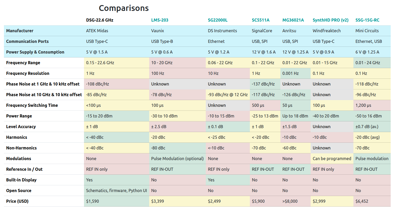
LMS-203, SG22000L, SC5511A, MG36021A, SynthHD PRO (v2), SSG-15G-RC
Manufacturer: ATEK Midas, Vaunix, DS Instruments, SignalCore, Anritsu, Windfreaktech, Mini Circuits
Communication Ports: USB Type-C, USB Type-B, Ethernet, USB, SPI, USB, SPI, USB Type-C, Ethernet, USB
Power Supply & Consumption: 5 V @ 1.5
explizit - an die Bedürfnisse der in der Abbildung gezeigten Module richtet. 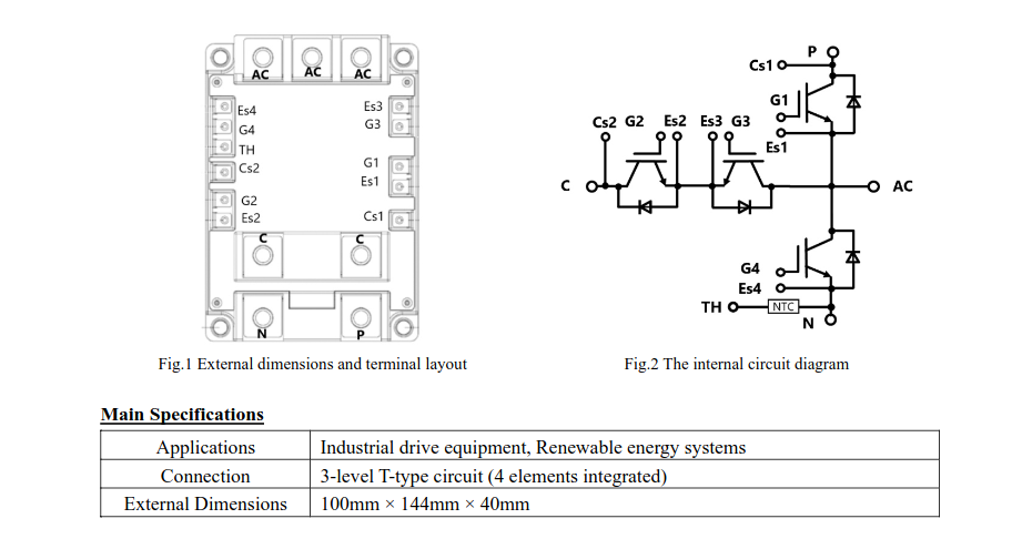 Bildquelle: Danfoss Zu den für Nutzer angebotenen Vorteilen vermeldet man dann das in der zweiten Abbildung gezeigte. 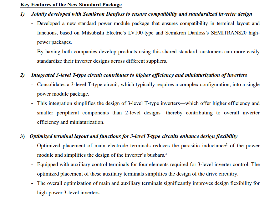 Bildquelle: Danfoss, beide via
BeagleV Ahead board uses an AP6203BM WiFi module connected to SDIO1. The Lichee Pi 4A has an RTL8723DS WiFi module also connected to SDIO1. The module reset line is driven through a PCA9557 GPIO expander on the I2C1 bus. --- https://lore.kernel.org/lkml/ah4lkWh2eD6l7W7n@x1/, via https://www.phoronix.com
FLA 206 Control unit A3 DMS Sense Low X6/1 Sense High Common Vref X6/2 + Input - Input X6/7 X6/5 X5 13 X6/6 14 Y X Y X A D S S Q D T Q R X8/1 Sense Low Sense High Common Vref + Input X8/2 s u - Input X8/7 B X8/5 T X7 A 13 X8 /6 e a 14 r Y X Y X A e D n S S I A10 13 14 13 14 Plug X13 X15 Q D T Q R X2 9
/ssl_tls13_client.c.obj [688/1714] Building C object esp-idf/mbedtls/mbedtls/library/CMakeFiles/mbedtls.dir/ssl_tls13_generic.c.obj [689/1714] Building C object esp-idf/mbedtls/mbedtls/library/CMakeFiles/mbedtls.dir
Packing) • Industrial Automation NFAQ1060L33T DIP38 400 / Box (Pb-Free) • Home Appliances ) , , ) ( ( ( DS 1 2 ( ( ( V V V V V T T P V V V HIN(U) HS1 LIN(U) LS1 HIN(V) Three channel HS2 HS1 HS2 HS3 half−bridge LIN(V) driver LS2 with HIN(W) protection HS3 LIN(W) circuits LS3 LS1 LS2 LS3 P V S O U R N N N C
Automation WW = Work Week • Home Appliances Device marking is on package top side ) )) ) ) ) ( (( DS 1 2 ( ( ( V V V V V T T P V V V ORDERING INFORMATION HIN(U) HS1 Shipping LIN(U) LS1 Device Package (Qty / Packing) HS1 HS2 HS3 HIN(V) Three channel HS2 NFAQ1560R43T DIP38 400 / Box half−bridge (Pb-Free
MOS-FET’S...............................................................................................13 4. WAVE FORMS OF THE LOGIC LEVELS...................................................................................................14 4.1 Shifting from a 3V to a 5V level............................

 Bild
Bild
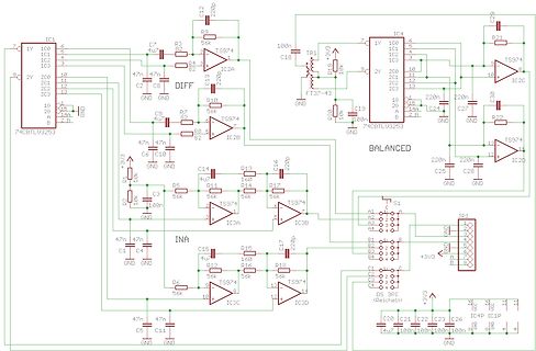
 Bild
Bild
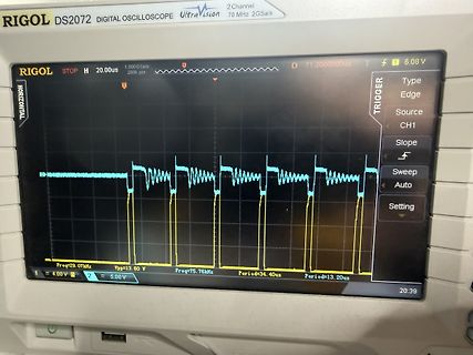
 Bild
Bild

 Bild
Bild
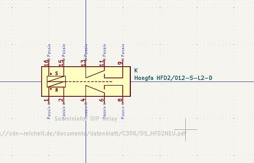
 Bild
Bild

 Bild
Bild
 Bild
Bild
 Bild
Bild
 Bild
Bild
 Bild
Bild