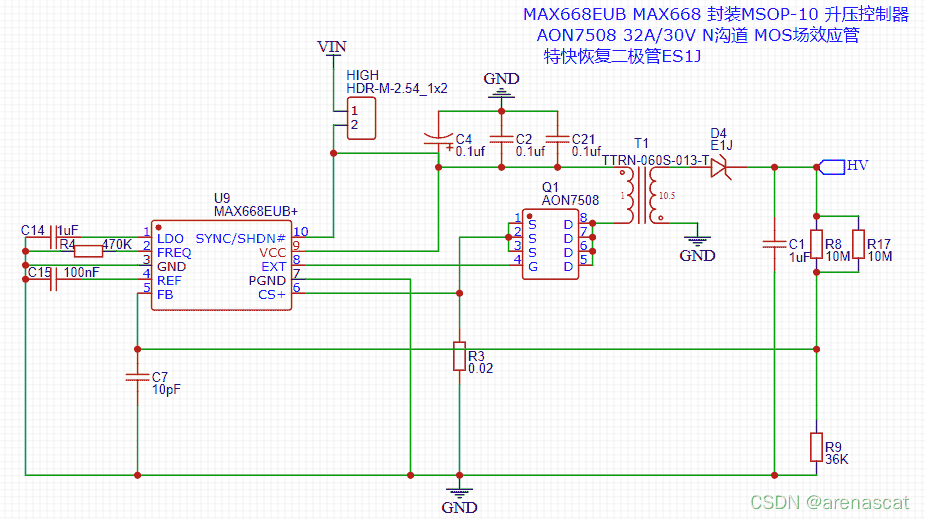
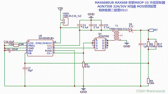
Chip antreibt. Sie unterscheidet sich von PGND und ist praktisch für die Hochspannungsisolierung. 4) REF ist ein Referenzspannungsausgang. Wenn er nicht verwendet wird, können auch andere ungefähre Kapazitäten gemessen werden. 5) FB ist der Feedback-Pin des Hochspannungseingangs. Zur Filterung wird hier
ground references may be at different potentials. Use with caution and avoid short circuits. 610-001247-02 A A A B C D E A B C D E 1 1 1 1 11 i C2 2 2 2 2 2 VB+ R R R R 330p VB(+) 330p R R R R R Ref Ref 5 5 5 5 5 5 5 5 5 5 2 2 2 2 2 Sig Sig 2 2 2 2 2 0 0 0 0 0 0 0 0 0 0 TP1a TP1b TP2b TP2a +5V i SwitchNode
XIN ELECTRONICS CO.,LTD SM2326E恒功率、 低THD高功率因数LED线性恒流控制芯片 QZSGIBV1.2 ESOP16 h c e - T i SyA1ol Mi0.02) c Ma0.08) b2 1.42 0.406 1.48 D n 9.80 0.203 9.85 E1 i 3.80 4.572 3.85 L2 X 0.35 2.413 0.65 u θ 0° 8° i J 注:如需最新资料或技术支持,请与我们联系 www.jiuxindzkj.com - 11 - JIU XIN ELECTRONICS CO.,LTD SM2326E恒功率、 低THD高功率因数
Unterspannung auf. 141 Personal Download for Hans-Jürgen Heidenreich | copyright Elektor 87 PR4401/02 im Doppelpack Leo Szumylowycz (D) Interessante Applikationen zu den ler Peripherie wünscht man sich manch- PR4401/02-Typen von PREMA gibt es mal noch einen etwas höherer Ausgangs- mittlerweileschoneinige
www.mikrocontroller.net/topic/261808#5532801 hab ich den ASSR-V621 gefunden: https://docs.broadcom.com/doc/AV02-0259EN https://de.aliexpress.com/item/32963227907.html (1,7€ pro Stück) Dieser Dual Channel Photovoltaic MOSFET Driver schafft 7V und die beiden genannten mosfet haben Gate Threshold Voltage 2-4
de.aliexpress.com/item/1005005899116574.html https://www.ti.com/lit/ds/symlink/lm74502.pdf?ts=1714137826663&ref_url=https%253A%252F%252Fwww.google.com%252F https://www.ti.com/lit/ab/slvafb3/slvafb3.pdf?ts=1714056386524&ref_url=https%253A%252F%252Fwww.google.com%252F Wenn die delays nur in microsecunden angegeben
Hi, V_ref und V_DD habe ich kontrolliert und beide sind bei ziemlich genau 5V (+/- 0.02V). Daten eingeben, funktioniert, soweit ich das mit Eingeben & Auslesen per Nak mit einer LED-Anzeige einschätzen kann
0,2V, wie er es nach Datenblatt sollte. > Bist du da um ein paar Zehnerpotenzen verrutscht? Ja 0,02V sollte das natürlich heißen. Danke für eure Hilfe! Dann hab ich jetzt einen Punkt, von dem ich weitermachen kann.
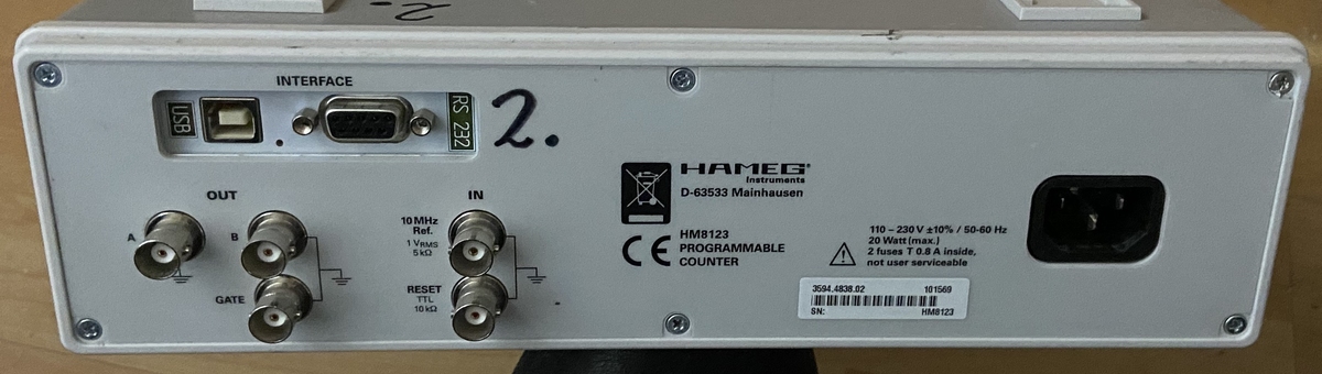
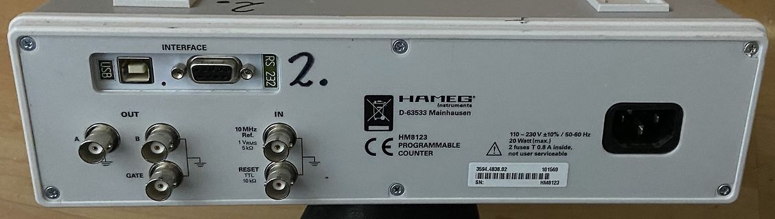
INTERFACE USB RS 232 2. OUT A B GATE RESET TTL 10 kOhm 10 MHz Ref. 1 VRMS 5 kOhm IN CE HM8123 PROGRAMMABLE COUNTER 110 - 230 V +/- 10% / 50-60 Hz 20 Watt (max.) 2 fuses T 0.8 A inside, not user serviceable 3594.4838.02 101569 SN: HM8123
altitude higher than 2000m(6500ft). ※Product Liability Disclaimer:For detailed information, please refer to https://www.meanwell.com/serviceDisclaimer.aspx File Name:IRM-01-SPEC 2023-02-20 1W Single Output Encapsulated Type IRM-01 series Block Diagram fosc : 130KHz EMI RECTIFIERS POWER RECTIFIERS +V I
bestimmten Zweck eine Schaltung sucht. https://www.ti.com/lit/wp/slyy062/slyy062.pdf?ts=1714290951143&ref_url=https%253A%252F%252Fwww.ti.com%252Fproduct%252Fde-de%252FLM5001 Natürlich bieten die ihr Zeug damit an, aber es steht auch viel Grundsätzliches in solchen Dokumenten.
August 2016 4 of 31 NXP Semiconductors PCA9532 16-bit I C-bus LED dimmer 6. Functional description Refer to Figure 1 “Block diagram of PCA9532”. 6.1 Device address Following a START condition, the bus master must output the address of the slave it is accessing. The address of the PCA9532 is shown in Figure
AMP VREF - SERIES PASS NOINPUT 5 + 10 VO REFT ERROR TRANSISTOR AMP +MP VREF 6 VOLT 9 V NON-INVERTING REF Z INPUT VOREGULATED OUTPUT V- 7 8 NC VZ CURRENT CURRENT LIMIT SENSE CA723C (CAN) V- TOP VIEW CURRENT LIMITER CURRENT LIMIT 10 TAB CURRENT 1 9 FREQ SENSE COMP V+ INPUTV 2 8 UNREG + INPUT NON-INV AMPOR
nicht ein optimales Beispiel sein, aber die vorige Ausgabe 0xeb 0x02 macht GAS leider nicht, sondern 0xe9 0x02 0x00 an der Adresse 0x2.
auf die schnelle) drei Links dazu gefunden: https://www.scs.stanford.edu/05au-cs240c/lab/i386/s16_02.htm https://stackoverflow.com/questions/14889643/how-encode-a-relative-short-jmp-in-x86 https://compas.cs.stonybrook.edu/~nhonarmand/courses/sp17/cse506/ref/assembly.html sprich: hängt sehr vom
0.20 e 0.10 n R1 R2 R3 R4 Ri (°C/W) τι (sec) o 0.1 0.05 R1 R2 R3 R4 s ττJ ττ 0.003454 13.68748 e 0.02 τ1 τ τ 0.17246 7.21E-05 l 1 2τ2 3τ3 ττ4 a 0.01 0.786312 0.001227 r Ci= τi/Ri 1.368218 0.007178 h 0.01 Ci i/Ri T SINGLE PULSE Notes: ( THERMAL RESPONSE ) 1. Duty Factor D = t1/t2 2. Peak Tj = P dm x Zthjc
jedes Beins ständig über von jedem Motor abgegebene Hall-Impulse berechnet. Die Beine einer einzelnen Refe- renz dürfen nicht mehr als +/- 5 Hall-Impulse unsynchron sein. Für ein Standard-Tischbein entspricht dies +/- 0,55 mm. »» Unterbrechungen an Motorkabeln werden ebenfalls als Fehler erkannt. oo Wenn
Architecture) programmer s interface. For information about low-level programming for the watchdog timer, refer to Application Note WdogP38x_E???.DOC, which you can request from Kontron technical support. For information about the JIDA programmer s interface refer to the JIDA BIOS extension section in the Appendix
and characteristics shown in this catalogue are subjected to modifications without notice. Always refer to ICEL S.r.l. web site, www.icel.it for products updated characteristics, last revision specifications, general data and information, products certifications and news. 0.2 Ed. 04 Rev. 02 12.2019 General
chip regularly. Users can just pull the SDN pin low all the time. 3. For more design details, please refer to “AN110 CMT221x-5x Schematic and PCB Layout Design Guideline. Table 7. BOM of Enhanced Anti-interference Typical Application Value (Match to λ/4 ANT) Designator Descriptions Unit Manufacturer 315
Anforderungen für einen Motor: Drehmoment: 10-15 Nm (Lagerreibungen?). Drehzahl: 10-12 U/min Leistung ca. 0,02 kW Soweit richtig? Grüße Bernd
einen Motor: > Drehmoment: 10-15 Nm (Lagerreibungen?). > Drehzahl: 10-12 U/min > Leistung ca. 0,02 kW stimmt. aber ein Schneckengetriebe das Selbsthemmend ist, hat normalerweise nicht mehr als 50% Wirkungsgrad. Ich denke dass es Sinn macht einen Schrittmotor für den Vorschub zu verwenden und
. Compensation output 6 ILoad Load current limitation Control 4 13 Overload 7 Csoft Soft start 8 V Ref Reference voltage 9 Mode Mode selection Comp. 5 12 High load 10 GND Ground 11 VS Supply voltage I 12 High load High load indication Load 6 11 VS 13 Overload Overload indication C GND 14 V Rö Ramp current adjust soft 7 10 15 V Sync. Voltage synchronization 16 Output Trigger output V Ref 8 9 Mode 95 11406 Series resistance 1 can be calculated as follows: ramp is determined by Cö and its charging currenö I . The charging current can be varied using Rö at Pin 14. The R 1max+ Vmains– V
white Sealing p/n 7158-3035 7158-3035 7158-3030-50 7158-3030-50 Pin p/n 7114-3250 7114-3250 7114-4102-02 7114-4102-02 Section [mm ]2 6.0 6.0 0.5 0.5 Table 6: Pinout description (*) For abbreviations see chapter Drive pin functions 8.2. NOTE: Never handle the fan module via the cable harness. All contents
H. schrieb im Beitrag #7629872: > Hg-Spektrum richtig anschauen! https://physics.nist.gov/PhysRefData/Handbook/Tables/mercurytable2.htm Die 185 kommen bei den wenigsten Lampen durch
-8708-kompatibilni-cssr-81735223.jpeg https://img.kleinanzeigen.de/api/v1/prod-ads/images/17/1789b02a-789c-4c3d-8665-a8980e33e5e5?rule=$_20.JPG /Versilbert/ aber waren sie im Westen, wenn überhaupt, dann nur sehr, sehr selten. Ich hab' mit meinen ersten EPROMs Anfang der 80er zu tun gehabt, aber
Aluguss-Gehäuse sind dafür gut geeignet. https://www.hammfg.com/electronics/small-case/diecast/1590z?referer=1353 ein alteingesessenes Unternehmen "In 1916, the company began in a backyard workshop in Guelph, Ontario, Canada." Die Gehäuse gibt es in vielen Größen zu kaufen, bis 400*230*180mm³
Eheschließung jünger sind als Männer https://www.destatis.de/DE/Presse/Pressemitteilungen/2024/02/PD24_N007_126.html Meine Mutter hat meinen Vater sogar um 30 Jahre überlebt (Altersunterschied bei Eheschließung: 14 Jahre).
tool chains. Please refer to this DVD-ROM, or to the Atmel web site, http://www.atmel.com/products/AT91/, for the most up-to-date information on getting started with the AT91SAM7A3-EK. Note that the AT91SAM7A3 microcontroller
transferred to the command register. For detail relationship 15 D/C# to MCU interface signals, please refer to the timing characteristics diagrams. When the pin is pulled high and serial interface mode is selected, the data at SDIN is treated as data. When it is pulled low, the data at SDIN will be transferred
Product Specification Part Name: OEL Display Module Customer Part ID: Allvision Part ID: QG-2832TSWEG02 Ver: A Customer: Approved by From: Allvision technology Inc. Approved by Allvision technology Inc. Http://www.szallvision.com Notes: 1.Please contact Allvision technology Inc. before assigning your product
is segment current reference pin. A resistor should be connected between this pin and V . Set the REF current lower than 12.5 μA SS Voltage output high level for COM signal 13 VCOMH This pin is the input pin for the voltage output high level for COM signals. A capacitor should be connected between this
: 0.635mm product. the physical information is inconsistent with the ordering information, please refer to the actual c - Address:Building B4,NO.777,Jianzhu Road,Binhu District,Wuxi City,Jiangsu Province 4/ 15 http://www.i-core. cn P.C.:214072 VER:2024-01-B1 Tab: 835-12-B4ORE Electronics Co., Ltd. Number
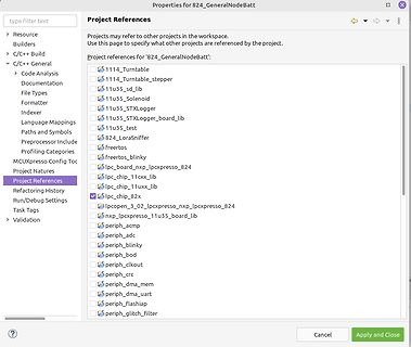
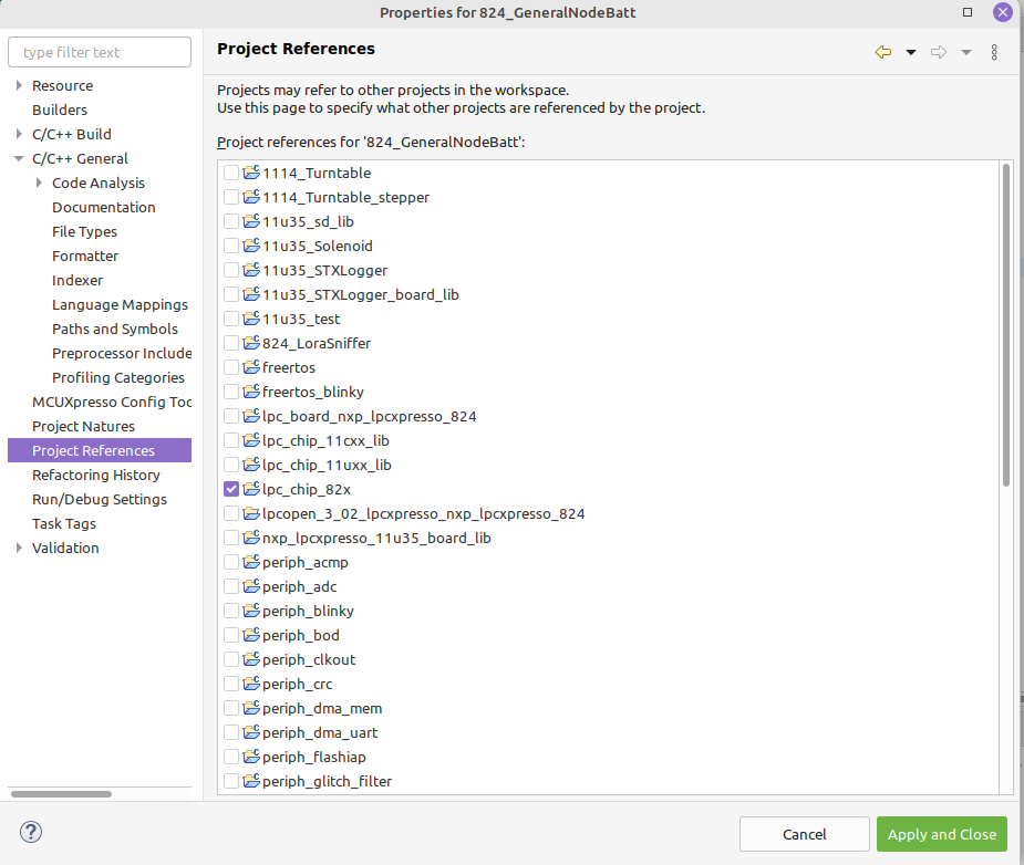
Properties for 824_GeneralNodeBatt
Projects may refer to other projects in the workspace.
Use this page to specify what other projects are referenced by the project.
Project references for '824_GeneralNodeBatt':
1114_Turntable
1114_Turntable_stepper
11u35
3 A/m Voltage dips, interruptions IEC/EN 61000-4-11 www.murata-ps.com/support D1U-H-2800-52-HBxC.B02 Page 3 of 5 D1U-H-2800-52-HBxC Series AC/DC Front End Power Supply OUTPUT CONNECTOR AND SIGNAL SPECIFICATION DC and Signal Connector: Tyco Part # 2-6450330-8, or FCI PowerBlade # 51939-180LF P1 P2 P3
the Timer/Counter0 Overflow interrupt is executed. The setting of this flag is dependent of the WGM02:0 bit setting. Refer to Table 14-8, “Waveform Generation Mode Bit Description” on page 103. 106 AT90USB82/162 7707F–AVR–11/10 AT90USB82/162 15. 16-bit Timer/Counter 1 with PWM The 16-bit Timer/Counter
out_mode_01 0 Use working temperature "T1" * out_mode_01 1 Use working temperature "T2" * out_mode_02 0 No identification. Temperature control by using the stored parameters. out_mode_02 1 Single identification of controlled system after the next start. out_mode_02 2 Continual identification of controlled
schrieb im Beitrag #7610007: > Die Berechnung erfolgt folgendermassen: > voltage = (adcValue * adcRefVoltage) / period; // ADC-Wert in eine Spannung umrechnen > adcRefVoltage = 3V > period = 4096 Du solltest also adcRefVoltage in deinem Code auf 3.3V ändern. Und laut Berechnungsformel im Datenblatt
schrieb im Beitrag #7610007: >> Die Berechnung erfolgt folgendermassen: >> voltage = (adcValue * adcRefVoltage) / period; // ADC-Wert in eine Spannung > umrechnen >> adcRefVoltage = 3V >> period = 4096 > > Du solltest also adcRefVoltage in deinem Code auf 3.3V ändern. Und laut > Berechnungsformel
0V to 2.6V. When it is form the COMP voltage, which is used to lower than the internal reference (REF), SS control the power MOSFET current. overrides REF so the error amplifier uses SS as the reference. When SS is higher than REF, During operation, the minimum COMP voltage REF regains control. is clamped

 Bild
Bild
 Bild
Bild
 Bild
Bild