-
PDF
STK625-728.pdf
possible.(Hi Active). • Single power supply drive is possible through the use of a built-in upper-side power-supply bootstrap circuit (Needs external capacitors). • Built-in simultaneous upper/lower ON prevention circuit to prevent arm shorting through simultaneous ON input for the upper and lower side
in „KI gefuehrte Fehlersuche an Waschmaschine Panasonic NA-168VG3“ · Analoge Elektronik und Schaltungstechnik ·
-
PDF
OWON_SDS_Series_-_Optimizing_Hardware_EN.pdf
into the case for it might be damaged when opening the case. The screws on the left and the right side differ a bit in length, be shure You know afterwards which screw belongs to which side. After removing the four screws there are additional snappers inside the case. One on the upper side und two on the down side. - 5 - OWON SDS Series – Optimizing the Hardware by BlueFlash - 6 - OWON SDS Series – Optimizing the Hardware by BlueFlash After opening the case You have to remove the switching supply. There is a
in „WELEC W2000A vs. OWON SDS8102“ · Mikrocontroller und Digitale Elektronik ·
-
PDF
Display_-_NL10276BC30-04D.pdf
1560 g (typ.) Contrast ratio 200:1 (typ.) Viewing angle (more than the • Horizontal: 65° (typ., left side, right side) contrast ratio of 10:1) • Vertical: 45° (typ., up side); 60 (typ., down side) Designed viewing direction • Widerviewing angle without image reversal : up side • Widerviewing angle withcontrast
in „VIA Nano Board LVDS Connector“ · Mikrocontroller und Digitale Elektronik ·
-
PDF
Display_-_NL10276BC30-04D.pdf
1560 g (typ.) Contrast ratio 200:1 (typ.) Viewing angle (more than the • Horizontal: 65° (typ., left side, right side) contrast ratio of 10:1) • Vertical: 45° (typ., up side); 60 (typ., down side) Designed viewing direction • Widerviewing angle without image reversal : up side • Widerviewing angle withcontrast
in „günstiges ITX Mainboard mit LVDS Connector“ · Mikrocontroller und Digitale Elektronik ·
-
PDF
LQ043T1DG01_SP_072106.pdf
Corporation Product No.: 6298 Bottom contact type) ※ The Bottom contact type can be selected according to side of mounted connector and terminal side of FPC. Terminal Signal Function No. 1 VLED- LED Power Source Input terminal (Cathode side) 2 NC No Connection 3 NC No Connection 4 VLED+ LED Power Source Input terminal (Anode side) 4-3.Touch panel 1mmP 4Pin FPC (Reference Connector: J.S.T. Mfg Co., Ltd, Product No.: 0.4(1.0)9FLH-SM1-GB-TB) Terminal No. Terminal name Description T1 YU Y (12 o’clock side) T2 XL X (left side) T3
in „Ansteuerung LQ043T1DG01“ · Mikrocontroller und Digitale Elektronik ·
-
PDF
VFD_Clock_Assembly_Manual_rev_3.pdf
Mount the 330 Ω resistors R1 ... R18 on the backside of the PCB. Mount the RGB LEDs on the front side of the PCB. Watch the polarity, the flat side of the LED goes where the PCB symbol is marked with a dash. Push the LEDs through the holes until they don't go any further. Be careful not to overheat
in „ESP32 DevKit-C“ · Mikrocontroller und Digitale Elektronik ·
-
PDF
n2pk_ad8307_power_meter.pdf
C5 use the above solid ground plane. output. This is displayed as 0 dB, within ground plane on one side and a section Trimming the module leads and about 0.5 dB, or essentially no meter of the metal plane on the other side. The keeping the components and wiring deflection. remainder of the split plane
-
PDF
LTC2945.pdf
2b. LTC2945 Derives Power from Figure 3b. LTC2945 Derives Power Through Low-Side a Wide Range Secondary Supply Shunt Regulator in High-Side Current Sense Topology GND RSHUNT V RSNS IN VOUT 0V TO 80V INTVCC SENSE + SENSE– VDD 2.7V TO 5.9V INTVCC C1 LTC2945 VDD LTC2945 GND C2 SENSE
in „U/I/P Metrer für Netzteile“ · Mikrocontroller und Digitale Elektronik ·
-
PDF
2945f.pdf
2b. LTC2945 Derives Power from Figure 3b. LTC2945 Derives Power Through Low-Side a Wide Range Secondary Supply Shunt Regulator in High-Side Current Sense Topology GND RSHUNT V RSNS IN VOUT 0V TO 80V INTVCC SENSE + SENSE– VDD 2.7V TO 5.9V INTVCC C1 LTC2945 VDD LTC2945 GND C2 SENSE
in „I2C mit Bascom Fehlersuche bei LTC2945“ · Mikrocontroller und Digitale Elektronik ·
-
 Bild
Bild
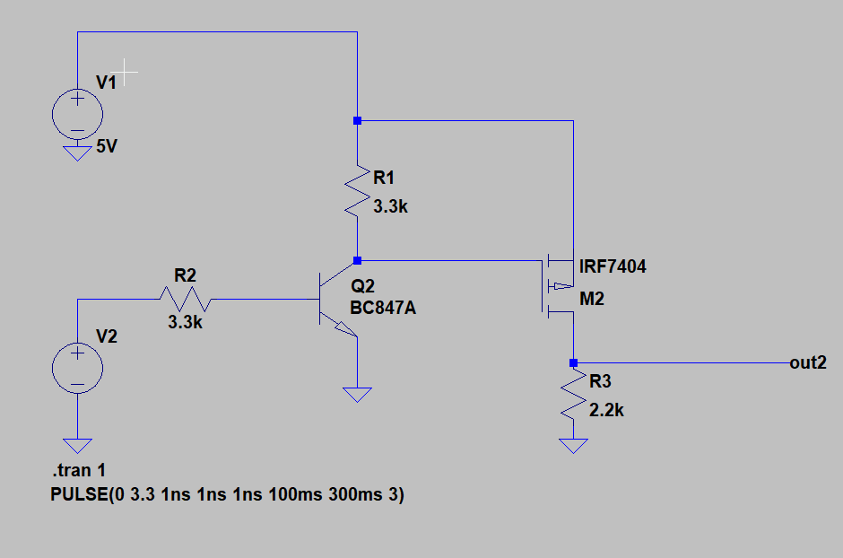
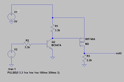
Schaltplan mit Transistor und MOSFET
V1 5V R1 3.3k Q2 BC847A R2 3.3k V2 IRF7404 M2 R3 2.2k out2 .tran 1 PULSE(0 3.3 1ns 1ns 100ms 300ms 3)
in „High Side Switch Mosfet“ · Analoge Elektronik und Schaltungstechnik · · Schaltpläne
-
 Bild
Bild
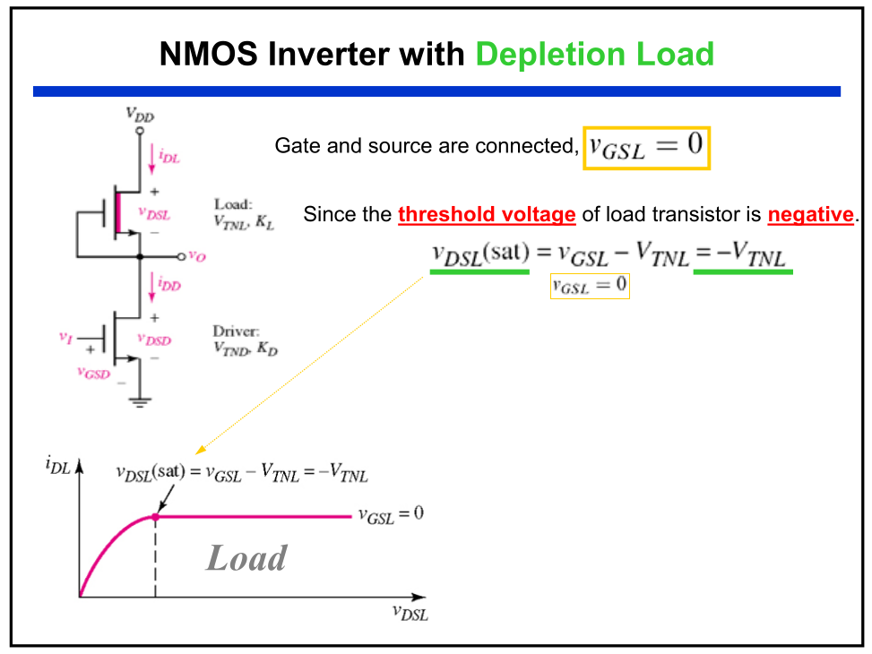
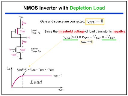
NMOS Inverter mit Depletion Load Erklärung
NMOS Inverter with Depletion Load VDD iDL + vDSL Load: VTNL, KL Gate and source are connected, vGSL = 0 Since the threshold voltage of load transistor is negative. vDSL(sat) = vGSL - VTNL = -VTNL vGSL = 0 vi + vDSD Driver: VTND, KD - VDD iDL vDSL(sat) = vGSL - VTNL = -VTNL vGSL = 0 Load vDSL
in „Schaltung mit 2 N-Kanal Mosfet“ · Analoge Elektronik und Schaltungstechnik · · Diagramme
-
 Bild
Bild
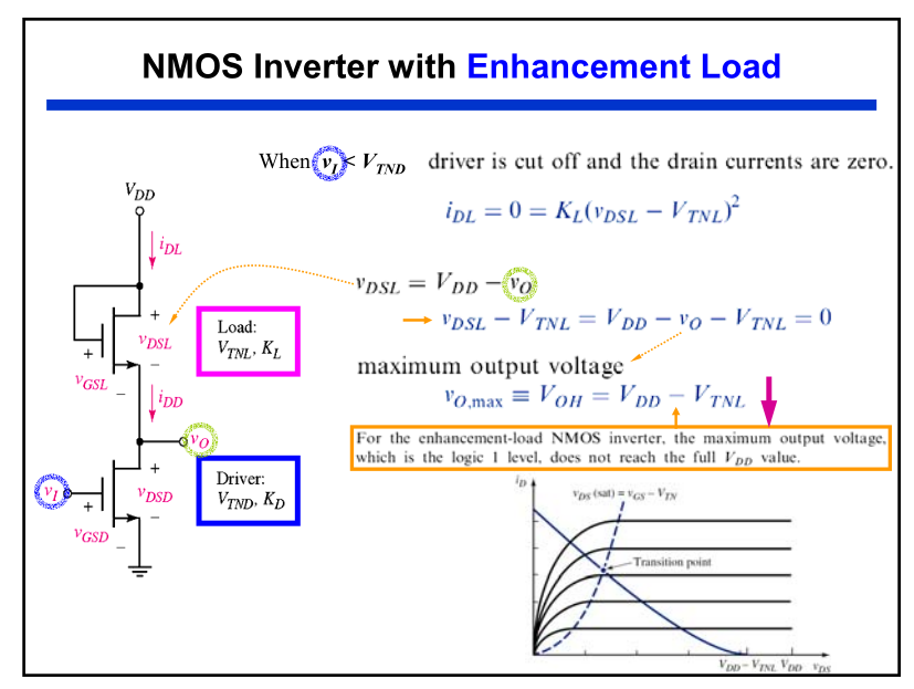
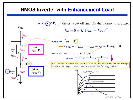
NMOS Inverter mit Enhancement Load Schaltplan und Kennlinie
NMOS Inverter with Enhancement Load When vI < VTND driver is cut off and the drain currents are zero. iDL = 0 = KL(vDSL - VTNL)^2 vDSL = VDD - vO vDSL - VTNL = VDD - vO - VTNL = 0 maximum output voltage vO,max = VOH = VDD - VTNL For the enhancement-load NMOS inverter, the maximum output voltage, which is the logic 1 level, does not reach the full VDD value. Load: VTNL, KL Driver: VTND, KD iD vDS (sat) = vGS - VTN Transition point vDD - VTNL vDD vDS
in „Schaltung mit 2 N-Kanal Mosfet“ · Analoge Elektronik und Schaltungstechnik · · Diagramme
-
PDF
drv8711.pdf
the time when driven at full current, or excessive power will be dissipated in the FET. During high-side turnon, the low-side gate is pulled low. This prevents the gate-source capacitance of the low- side FET from inducing turnon. The predriver circuits include enforcement of a dead time in analog circuitry
in „UV-Laserdrucker II“ · Platinen ·
-
PDF
lm5642.pdf
connection. It serves as the positive supply rail for the Channel 2 top-side gate drive. Connect this pin to VDD2 (Pin 19) through a diode, and connect the low side of the bootstrap capacitor to SW2 (Pin16). VDD2 (Pin 19) The supply rail for the Channel 2 low-side gate drive
in „Komisches Verhalten von LM5642MTCX“ · Analoge Elektronik und Schaltungstechnik ·
-
PDF
ADC_DelSig_v3_20.pdf
. Side Effects: None int8 ADC_Read8(void) Description: This function simplifies getting results from the ADC when only a single reading is required. When called, it will start ADC conversions, wait for the
in „Dev-Board mit mind. 4 x Delta-Sigma-ADC & CAN-BUS“ · Mikrocontroller und Digitale Elektronik ·
-
PDF
drv8833.pdf
IOUT(RMS) (2) where P TOT is the total power dissipation, HS - RDS(ON) is the resistance of the high side FET, LS - R DS(ON) is the resistance of the low side FET, and I OUT(RMS) is the RMS output current being applied to the motor. Note that R DS(ON)increases with temperature, so as the device heats, the
in „TI DRV8833 Muss man den PWM Pin wechseln?“ · Mikrocontroller und Digitale Elektronik ·
-
PDF
Speedballmanual_02-03-14.pdf
PC board with two #4 x ¼" screws. Attach and solder the red wire from 2U to the B+ pad on the left side of the PC board. 24 Attach and solder the black wire from 7L to the O pad on the left side of the PC board. Attach and solder the black wire from 3U to the G pad on the right side of the PC board. Attach
in „150V DC für Röhrenverstärker erzeugen“ · Analoge Elektronik und Schaltungstechnik ·
-
Datei
main.c
** * Function: void RestoreEEPromValues(void) * PreCondition: None * Input: None * Output: None * Side Effects: None * Overview: Restores the Factory State to all available CVs * CV1 CV2 CV3 CV4 CV5 CV7 CV8 CV11 * (0x03, 0x00, 0x07, 0x07, 0x7F, 0x7F, 0xA5, 0xFF); * CV19 CV29 CVx CVx CVx CVx CVx CVx *
in „DCC Lokdecoder PIC16F628“ · Mikrocontroller und Digitale Elektronik ·
-
PDF
PCB_Design_Optimization_Starts_in_the_CAD_Library.pdf
Styles Ball Grid Array Bump Grid Array Bottom Grid Array Column Grid Array Pillar Grid Array Flat Side Convex Side Concave Side Corner Concave Inward L Gull Wing Outward L J-Lead End Cap Under Body L Flat Flat Bottom No-Lead Through-hole Rounded Rectangular Land Shape Used For These Component Lead
in „Altium Mechanical Layer 13 und 15“ · Mikrocontroller und Digitale Elektronik ·
-
PDF
SM-Oven.pdf
Using a clean, dry cloth, insert the new bulb. 5. Reinsert the bottom of the glass cover (smooth side out) into the bottom clip, and firmly push the top of the cover into the upper clip until it snaps into place. 6. Restore power to the unit. 4.3.1.2 Halogen Side Lamp (Horizontal-style) 1. Remove racks
in „Einbaubackofen streikt mit Fehlercode E 101“ · Haus & Smart Home ·
-
Datei
ADC_Interface.vhd
std_logic; --enable_in : in std_logic; Real_in_from_ADC : in std_logic_vector(9 downto 0);--receiver side i/p -- imag_in_from_ADC : in std_logic_vector(9 downto 0); --receiver side i/p Dout : out std_logic_vector(9 downto 0);--receiver side 0/p -- Dout2 : out std_logic_vector(9 downto 0);--receiver side
in „Programmieren des LTC2287 Dual 10-Bit ADCs“ · FPGA, VHDL & Co. ·
-
PDF
Apex_MSA240.pdf
portion of the PCB layout does not pass over low-level R K L 2 A analog signal traces on the opposite side of the PCB. Capacitive C C K R C coupling through the PCB may inject switching voltages into the PWM AMPLIFIER analog signal path. Further, make sure that the power side of the PCB layout does not come close to the analog signal side. Fast rising output signal can couple through the trace-to-trace FIGURE 1. EXTERNAL OSCILLATOR CONNECTIONS capacitance on the same side of the PCB. SHUTDOWN DETERMINING THE OUTPUT STATE The MSA240 output
in „Linear-Amp oder PWM Amp mit H-Brücke?“ · Analoge Elektronik und Schaltungstechnik ·
-
PDF
IGBT_Gate.pdf
windingofthepowertransformerisusedtodrivethe turning on T2, and clamping the voltage at point P, high side switch as a synchronized slave of the causing D to become reverse biassed. Turning on T2 causes Zener Z2 to clamp the IGBT gate voltage grounded low side switch; when the low side switch at 6V, limiting
in „Abschaltvorgang IGBT - Frage“ · Analoge Elektronik und Schaltungstechnik ·
-
PDF
Optical-Incremental-Encoder-Modules.pdf
6 MountingConsiderations * 3. * FOR WINDOW OPTION MEASUREMENT = 3.22 (0.127) Figure2.MountingPlaneSideA. Figure3.MountingPlaneSideB. Figure4.MountingasReferencedtoSideA. Figure5.MountingasReferencedtoSideB. 7 Connectors Mounting Manufacturer PartNumber Surface AMP 1203686-4 Both 640442-5 Side B DuPont 65039-032 with Both 4825X-000 term. HP HEDS-8902 Side B with 4-wire leads (see Fig. 6) Molex 2695 series with Side B 2759 series term. Figure6.HEDS-8902Connector. OrderingInformation HEDS-9000 Option 0 0 HEDS-6100 Option Resolution ShaftDiameter (Cycles
in „Inkrementalgeber HEDS 9000, TTL, Impulsmessung“ · Mikrocontroller und Digitale Elektronik ·
-
PDF
TTester_096k.pdf
combinations of measurement 14 4.1 Measurement of Semiconductors One probe pin is assumed to be the negative side of the component. Another pin is assumed to be the positive side of the component. For a ▯rst test, the components positive side is directly connected to VCC. The negative side is connected with the
-
PDF
TTester_096k.pdf
combinations of measurement 14 4.1 Measurement of Semiconductors One probe pin is assumed to be the negative side of the component. Another pin is assumed to be the positive side of the component. For a ▯rst test, the components positive side is directly connected to VCC. The negative side is connected with the
-
PDF
bd623x.pdf
1.2 1.6 2 Output Current: IOUT [A] Output Current: IOUT [A] Output Current: IOUT [A] Fig.16 High side body diode (0.5A class) Fig.17 High side body diode (1A class) Fig.18 High side body diode (2A class) 0.8 1.6 2 85°C 85°C 85°C 25°C 25°C 25°C ] -40°C ] -40°C ] -40°C [ 0.6 [ 1.2 [1.5 T T T O O O : :
in „2x Motoren (12V / 2A) mit PWM ansteuern (µC PIC)“ · Mikrocontroller und Digitale Elektronik ·
-
PDF
LSIsforLCDs.PDF
*1 New drive technology : A drive technology which drives LCDs with low voltage of 5 V on segment side, and drives LCDs with high voltage on common side. Driving with low voltage on segment side enables LCDs to reduce power consumption and shadowing. *2 Conventional drive technology : A drive technology
in „LEXIBOOK LCD-Konsole mit 120 Spiele“ · Mikrocontroller und Digitale Elektronik ·
-
PDF
4fach_7segment.pdf
tinted green segments or untinted segments. Package Dimensions 88:88 0.56" Four Digit Display FRONT SIDE RIGHT SIDE 2 – ∅1.70 7.80 (0.067) (0.307) 10.00° PIN 12 PIN 8 + + A A A A B B DP3 F 6.00 14.22 19.10 15.24 F G F G G B F G B (0.236) (0.560) (0.752) (0.600) E C E C E CE C DP2 + + D D D D PIN 1 PIN
in „7 Segment Anzeige - SAA1064 + 4stellige Anzeige“ · Mikrocontroller und Digitale Elektronik ·
-
PDF
semi_eng_aqh-1299268.pdf
Tube Tape and current style style Picked from the Picked from the reel state voltage 1/2/3/4-pin side 5/6/8-pin side 0.3 A AQH0213 AQH0213A AQH0213AX AQH0213AZ 0.6 A AQH1213 AQH1213A AQH1213AX AQH1213AZ 0.9 A Zero-cross AQH2213 AQH2213A AQH2213AX AQH2213AZ 1 tube contains AC 1.2 A AQH3213 AQH3213A AQH3213AX
in „Ansteuerung von ElTako (Stromstoßschalter)“ · Haus & Smart Home ·
-
PDF
lcd_datasheet.pdf
designing-stage as below: ‧ The degrees of unbalance: < 10% ‧ The ratio of wave heigh:<√ 2 ±10% Ip Ip:high side peak I-p I-p:low side peak A:The degrees of unbalance =︱Ip – I-p︱/ Irms ×100 (%) B:The ratio of wave height = Ip (or I-p) / Irms *2) Lamp Current measurement method (The current meter is inserted in
in „Laptop LCD inverter board frage“ · Analoge Elektronik und Schaltungstechnik ·
-
PDF
CLAA154WA05AN_ASUS_A6JC_display.pdf
designing-stage as below: ‧ The degrees of unbalance: < 10% ‧ The ratio of wave heigh:<√ 2 ±10% Ip Ip:high side peak I-p I-p:low side peak A:The degrees of unbalance =︱Ip – I-p︱/ Irms ×100 (%) B:The ratio of wave height = Ip (or I-p) / Irms *2) Lamp Current measurement method (The current meter is inserted in
in „Laptop LCD ansteuern wollen // FPGA einstieg ?“ · Mikrocontroller und Digitale Elektronik ·
-
PDF
p200912.pdf
and 1.3-in height. The distance between the centers of the resonators to each of the three closest side walls along the orientation of the resonator is fixed, which is always half of the cavity width. For example, the distance between the center of resonator 1 to each of the three vertical side walls is
in „Topfkreis - Leistungsdimensionierung“ · HF, Funk und Felder ·
-
PDF
3999fa-1.pdf
a square wave voltage pulse on the of the cycle. Leaving the ILIM/SS pin unconnected will primary side of a center tapped transformer. The diodes disable the programmable current limit and the LT3999 on the secondary side rectify the voltage and generate will default to its internal current limit. the
in „Halbbruecke Fragen“ · Analoge Elektronik und Schaltungstechnik ·
-
PDF
info-uiir2156.pdf
measured under board mounted and still air conditions. Symbol Definition Min. Max. Units VB High side floating supply voltage -0.3 625 VS High side floating supply offset voltage VB- 25 VB+ 0.3 V High side floating output voltage V - 0.3 V + 0.3 V HO S B VLO Low side output voltage -0.3 V CC+ 0.3 IOMAX
in „Leuchtstoffröhren Vorschaltgerät 24V Reparatur-Tipp gesucht“ · Fahrzeugelektronik ·
-
 Bild
Bild
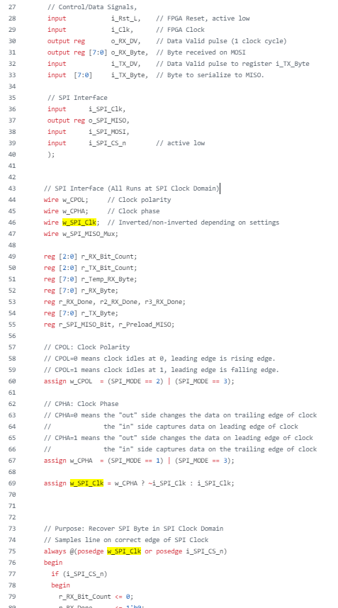
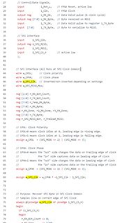
Programmcode für eine SPI-Schnittstelle
(SPI_MODE == 2) | (SPI_MODE == 3); 61 62 // CPHA: Clock Phase 63 64 65 // CPHA=0 means the "out" side changes the data on trailing edge of clock 66 // the "in" side captures data on leading edge of clock 67 // CPHA=1 means the "out" side changes the data on leading edge of clock 68 // the "in" side
in „FPGA als SPI Slave“ · FPGA, VHDL & Co. · · Screenshots
-
PDF
TFDS4500_69428.pdf
Capable of Surface Mount PCs, Palmtop Computers (Win ▯ Wide Operating Voltage Range Solderability to Side- and CE, Palm PC), PDAs (2.7 to 5.5 V ) Top-View Orientation ▯ Digital Still and Video Cameras ▯ Low Power Consumption ▯ Directly Interfaces with Various ▯ Printers, Fax Machines, (1.3 mA Supply Current
in „Pollin Netbox“ · Mikrocontroller und Digitale Elektronik ·
-
Datei
xlcd.c
********* * Function : void XLCDInit(void) * PreCondition : None * Input : None * Output : None * Side Effects : None * Overview : LCD is intialized * Note : This function will work with all Hitachi HD447780 * LCD controller. ********************************************************************/ void
in „PIC 18f2550 und LCD mittels Maestro“ · Mikrocontroller und Digitale Elektronik ·
-
 Bild
Bild
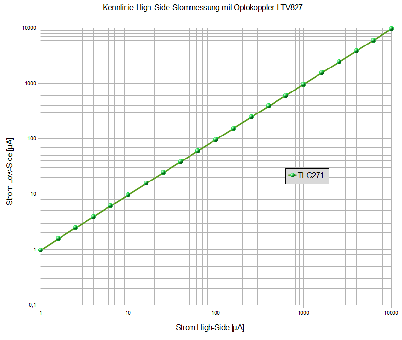
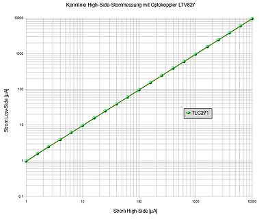
Kennlinie High-Side-Strommessung mit Optokoppler LTV827
Kennlinie High-Side-Strommessung mit Optokoppler LTV827 10000 1000 100 10 1 0,1 Strom Low-Side [µA] Strom High-Side [µA] TLC271
in „Isolierte Spannungsversorgung“ · Analoge Elektronik und Schaltungstechnik · · Diagramme
-
 Bild
Bild
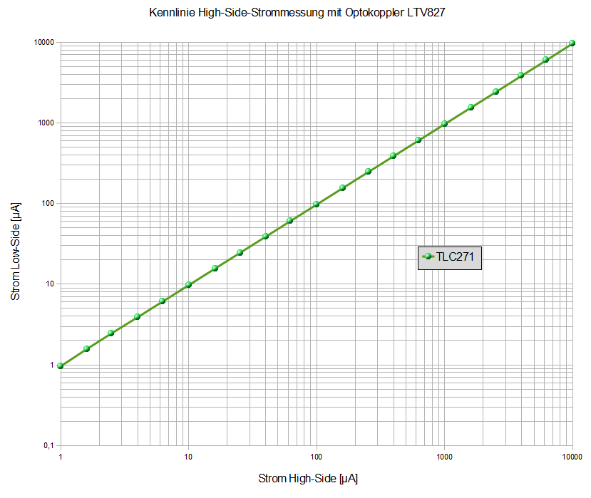
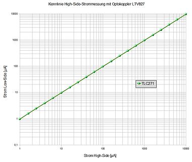
Kennlinie High-Side-Strommessung mit Optokoppler LTV827
Kennlinie High-Side-Strommessung mit Optokoppler LTV827 10000 1000 100 10 1 0,1 Strom Low-Side [µA] 1 10 100 1000 10000 Strom High-Side [µA] TLC271
in „Lineare High-Side-Strommessung mit Optokopplern“ · Analoge Elektronik und Schaltungstechnik · · Diagramme
-
PDF
rs232_datasheet.pdf
electronics where sensible computer equipment needs to be protected. All inputs (primary and secondary side) are protected against ESD and withstand 15kV discharges on the human body model. The secondary side RS232 input and supply voltages range from 1.8V to 5.5V. Input and supply voltages Overview need to be matched. The secondary side current consumption is <20mA at 1.8V, reducing to <10mA @ 3.3V. A true-green LED shows presence of supply Primary power. Only RX and TX signals are isolated. All other Chipset FT231 RS232 signals are
in „[V]USB to RS232 Isolator & Voltage Translator“ · Markt ·
-
PDF
rs232_datasheetv2.pdf
electronics where sensible computer equipment needs to be protected. All inputs (primary and secondary side) are protected against ESD and withstand 15kV discharges on the human body model. The secondary side uart input and supply voltages range from 1.8V to 5.5V. Logic Level and supply voltages need to be matched. The secondary side Overview current consumption is low. A true-green LED shows Primary presence of supply power. Only RX and TX signals are isolated. All other RS232 signals are not available. Chipset FT231 The primary-side
in „[V]USB to RS232 Isolator & Voltage Translator“ · Markt ·
-
PDF
GLCD_unit_testboard_V1.pdf
1 VCC P3 1 2 1 VSS 0 1 3 4 2 9 D VDD 7 PWR_FLAG Contr. 5 6 3 Contr. S VCC RS/CS 7 8 4 RS/CS 0 _ RW/SID 9 10 5 2 6 P1 RW/SID 9 8 2 1 E/CLK 11 12 6 E/CLK 7 2 Contr. 4 3 RS/CS DB0 13 14 7 DB0 T _ RW/SID 6 5 E/CLK DB1 15 16 8 DB1 S D DB0 8 7 DB1 DB2 17 2 18 9 _ L 0 DB2 4 G DB2 10 X 9 DB3 DB3 19 2 20 10DB3
in „KiCad - Luftlinie für nicht vorhandene Verbindung“ · PC Hard- und Software ·
-
PDF
MegaBoardV1.4.pdf
Atmel Experimentier Board V1.4 erstellt von Ulrich Radig Single Side AVR Experimentier Board Version 1.4 erstellt von Ulrich Radig 1 Atmel Experimentier Board V1.4 erstellt von Ulrich Radig Inhaltsverzeichnis: 1. Vorwort S.3 2. Spezifikation S.4 3. Beschreibung S.5 4
in „ATMEGA128 funzt nicht“ · Mikrocontroller und Digitale Elektronik ·
-
PDF
t69b1.pdf
provide power to the PIC, therefore the Pgm Header board must be powered while programming. the top side of 20Mhz resonator Vpp n/c Pgc Pgd Gnd the pcb Reset 1uf 1uf u Pin1 f Pin1 I 2 4.7k m u R IC1 PIC mcu u L The female 2x10 header must be D f 2 t D mounted from the BOTTOM side of he 9 2 o H F m a pcb
in „LCD240128A an PIC 18F4550“ · Mikrocontroller und Digitale Elektronik ·
-
PDF
Datasheet-HE144-20120601.pdf
Offset Voltage, up I1= I1N B = 0 T 1.0 sec to 3 min. after power ∆ V 0 not specified mV up Supply side internal resistance , B = 0 T R10 900...1250 Ω typical 1000 Temperature coefficient of the Supply side TC R10 typical 0.35 %/K internal resistance, B = 0 T Hall side internal resistance , R20 900...1700 Ω B = 0 T typical 1000 Temperature coefficient of the Hall side TC R20 typical 0.35 %/K internal resistance, B = 0 T Linearity of Hall voltage B = 0…0.5 T ∆ V < ± 0.2 % 20-0.5 (or L-0.5 typical ≤ ± 0.1 B = 0…1.0 T ∆ V20-1 ≤ ± 0.2 % (or L-1 typical ≤ ± 0.1 B = 0…
in „"Hallsonde für Oszilloskop" im Eigenbau?!“ · Analoge Elektronik und Schaltungstechnik ·
-
PDF
uTracer3plus_con_man.pdf
components to the PCB, allow for some time to let the solder flow through the contact holes to the front side of the PCB. This will create an additional conductive path between front- and back-side contact pad. 7. The PCB is designed for both standard size 5 mm pitch Xtals as well as miniature 2.5 mm pitch
in „Röhrenprüfer/ Kennlinienschreiber utracer kaputt“ · Analoge Elektronik und Schaltungstechnik ·
-
PDF
drag_specialties_mini_tach_pn_2211-0057005801190120.pdf
the light terminal on the ignition switch. 4. Connect the green wire on the tach to the negative side of the coil, the tach lead on the ignition, or to a tach adapter ▯▯▯▯Y▯RU▯/LJKW▯FLUFXLW depending on your application. The negative side of the coil ▯▯▯▯Y ▯▯▯▯Y is the side leading to the ignition module. (On stock bikes this is usually a blue or pink wire.) The positive side of the coil supplies 12 volts from the ignition switch. 7$&+20(7(5▯:▯/('▯,//80,1$7('▯)$&( WARNING!: Before operating the motorcycle, be sure all hardware is tight. 3501 Kennedy Rd, PO Box 5222, Janesville
-
PDF
klassed_facharbeit.pdf
38. Der Lowside Mosfet wird tollerierbare Stromspitze. ausgeschaltet und der Hi side eingescahltet. Der Ch1: Gatespannung HI-Side Mosfet Vorgang läuft korrekt ab. Ch2: Gatespannung Low-Side Mosfet Ch1: Gatespannung HI-Side Mosfet Ch2: Gatespannung Low-Side Mosfet Abbildung 40: Völlig
in „Suche Schaltplan für PWM Endstufe“ · Mikrocontroller und Digitale Elektronik ·
-
PDF
MP2363_r1.3.pdf
Voltage Gain AVEA 400 V/V Error Amplifier Transconductance G EA ∆ICOMP= ±10µA 500 800 1120 µA/V High-Side Switch On-Resistance (4) R DS(ON)1 100 mΩ Low-Side Switch On-Resistance R DS(ON)2 6 Ω High-Side Switch Leakage Current V = 0V, V = 0V 0.1 10 µA EN SW Short Circuit Current Limit 4.5 5.7 A Current Sense
in „Schaltregler gesucht“ · Mikrocontroller und Digitale Elektronik ·