function Explanation Low voltage protection Below the minimum voltage value for normal operation of the inverter. Overload protection The load exceeds the rated overpower. High voltage protection Higher than the maximum voltage
Hier sind ein paar Tips zur Messung: https://www.flir.com/de-de/discover/rd-science/use-low-cost-materials-to-increase-target-emissivity/
Übersetzung.. hier der Link zum englischen Artikel: https://www.flir.com/discover/rd-science/use-low-cost-materials-to-increase-target-emissivity/ HTH und nix für Ungut
. Daher auch die Anforderung der Messung kleiner Ströme nur bin ich nicht sicher ob das besser Low Side oder High Side gemacht werden soll. Die Isolation hat mich bei der Planung bisher eher zu dem Scgluss gemacht es auf der Low Side zu machen.
stm32wba25ce.pdf Im Bereich des Funkmoduls hebt STMicroelectronics die folgenden Attribute hervor: [c] High‑performance radio delivering stable connectivity with +10 dBm max output power Supports Bluetooth® LE, Zigbee, and Thread for broad protocol compatibility Programmable Tx power in 1 dB steps
precisely tune energy consumption and extend battery life Flexible power‑control leveraging ultra-low-power STM32 MCU architecture for longer battery life [/c] Interessant ist, dass sich im Abschnitt zu den geringen Kosten nach folgendem Schema auch ein Hinweis auf die Optimierung des Layouts
bandpass circuit as shown in Figure 11 10k 15(a), can be used. 470k Figure 13. MC1377 Output with VB Low Resolution RGB Inputs X X X X Figure 12. Delay of Chroma Information a G Luminance 1.0 2.0 3.0 3.58 4.0 5.0 (a) Encoder Output with Low Resolution Inputs Chroma and No Bandpass Transformer The Chroma
CA-C03 Specifications Features 1. Small size SMD patch antenna with size only 5.5 X 2.0 X 1.0 mm. 2. Low energy loss, high antenna efficiency. 3. High stability under temperature and humidity changes. Structure 1. Antennafeeder 2. Feeder identificationmark 3. Antenna welding fixed end Size Three View symbol
data is received by the UART and an RX Timeout occurs // This is a callback function executed from a high priority monitor task // All data will be buffered into RX Buffer, which may have its size set to whatever necessary void fill_UART_RX_Buffer() { uint8_t i=0; while (Serial.available()) { uart_buffer
manchen Dingen "befremdlich" aus, ein "digitalWrite" ... herjeh... und dann auch noch eine Angabe von "HIGH" und "LOW"... anstelle von 1 und 0 (ich weiß, dass ich auch 1 und 0 angeben kann). Aber das ist eben der Lauf der Dinge, wie heute Sachen verstanden werden (das ist jetzt keine Wertung von positiv
Das unbekannte IC im PDF ist ein High/Low Side Gate Treiber. C14 und D1 sind die Charge Pump für den oberen Transistor, da sollten ca. 10V relativ zum Mittelabgriff zwischen den Ausgangstransistoren anliegen. Die DC Messwerte an allen
USB 2.0) Usb300 : 0 (no, port not supports USB 3.0) ReservedMBZ : 0x00 Flags : 0x00 DevIsOpAtSsOrHigher : 0 (Device is not operating at SuperSpeed or higher) DevIsSsCapOrHigher : 0 (Device is not SuperSpeed capable or higher) DevIsOpAtSsPlusOrHigher : 0 (Device is not operating at SuperSpeedPlus or higher) DevIsSsPlusCapOrHigher : 0 (Device is not SuperSpeedPlus capable or higher) ReservedMBZ : 0x00 ---------------------- Device Descriptor ---------------------- bLength : 0x12 (18 bytes) bDescriptorType : 0x01 (Device Descriptor
USB 2.0) Usb300 : 0 (no, port not supports USB 3.0) ReservedMBZ : 0x00 Flags : 0x00 DevIsOpAtSsOrHigher : 0 (Device is not operating at SuperSpeed or higher) DevIsSsCapOrHigher : 0 (Device is not SuperSpeed capable or higher) DevIsOpAtSsPlusOrHigher : 0 (Device is not operating at SuperSpeedPlus or higher) DevIsSsPlusCapOrHigher : 0 (Device is not SuperSpeedPlus capable or higher) ReservedMBZ : 0x00 ---------------------- Device Descriptor ---------------------- bLength : 0x12 (18 bytes) bDescriptorType : 0x01 (Device Descriptor
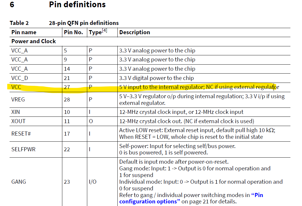
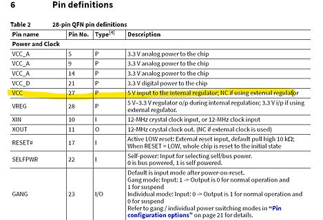
clock input
XOUT 11 O 12-MHz crystal clock out. (NC if external clock is used)
RESET# 17 I Active LOW: External reset input, default pull high 10 kΩ; When RESET = LOW, whole chip is reset to the initial state
SELFPWR 22 I Self-power: Input for selecting self/bus power. 0 is bus powered, 1 is self powered
CY7C65642 EZ-USB™ HX2VL low-power multiple transaction translator USB 2.0 hub controller Features • High-performance,low-power USB2.0hub,optimized for low-cost designs with minimumbill-of-material (BOM). • USB 2.0 hubcontroller
zum Übersetzen und Flashen des Controllers habe ich auch hinzugefügt, der ATtiny hat Fusesettings: LOW: 0xE4, HIGH: 0xDF, EXT.: 0xFF. Dieses entspricht einem Takt von 8 MHz intern, der Chip benötigt also keinen externen Quarz. Wer es brauchen kann: bitte bedienen! Gruß, Ralph
auf 0 und umschalten nur über DDR habe ich gemacht und funktioniert: [code] #define i2c_setpins_low() { i2c_port &= ~(1<<sda_bit); i2c_port &= ~(1<<scl_bit); } #define sda_high() (i2c_ddr &= ~(1<<sda_bit)) #define sda_low() (i2c_ddr |= (1<<sda_bit)) #define scl_high() (i2c_ddr &= ~(1<<scl_bit
has higher impact with 4 programmed levels MLC can store twice the bits per square mm Cost high medium low silicon Swissbit AG Revision: 1.04 Industriestrasse 4 TLP: Swissbit public Template: Doc-4991 CH-9552
Ladungsverstärker, Instrumentenverstärker, ....). Alles mit Antenne oder Ton lieber symmetrisch. Und für die High-Side Strommessung mit OP und Transistor brauchst Du quasi einen anderen OP, der auf der High-Side an seinen Rail kommt (Ja, es gibt auch Rail to Rail, aber die kommen mit anderen Nachteilen) Früher
Instrumentenverstärker, ....). > > Alles mit Antenne oder Ton lieber symmetrisch. Und für die High-Side > Strommessung mit OP und Transistor brauchst Du quasi einen anderen OP, > der auf der High-Side an seinen Rail kommt (Ja, es gibt auch Rail to > Rail, aber die kommen mit anderen Nachteilen
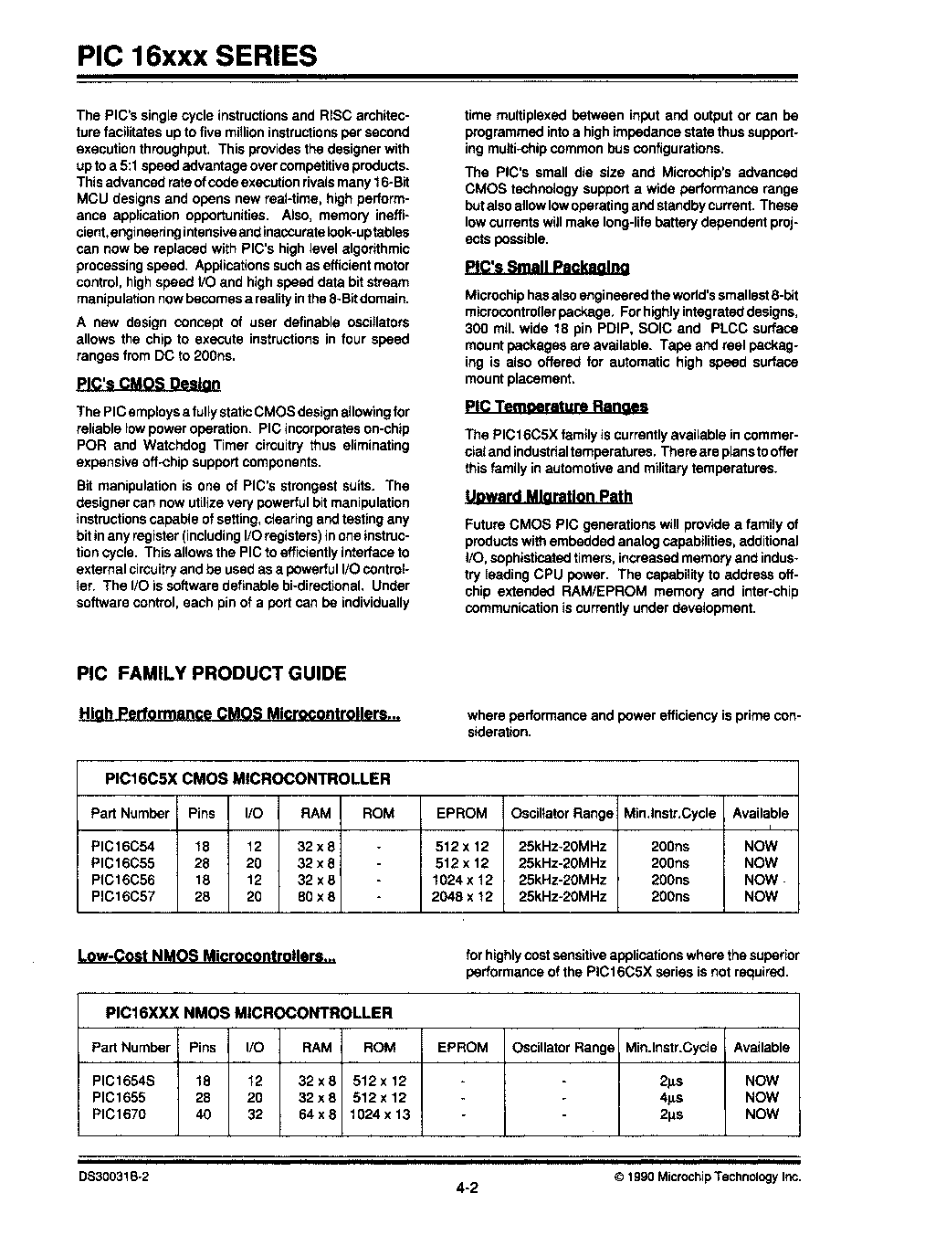
Design
PIC's Small Packaging
PIC Temperature Ranges
Upward Migration Path
PIC FAMILY PRODUCT GUIDE
High Performance CMOS Microcontrollers...
PIC16C5x CMOS MICROCONTROLLER
Part Number Pins I/O RAM EPROM Oscillator Range Min.Instr.Cycle Available
PIC16C54 18 12 32 x 512 x 25kHz-20MHz 200ns NOW
PIC16C55
Sensors, wenn der Elektronenstrahl und Masse zu schalten; Rxx setzt die Widerstandsänderung in einen LOW-ng Impuls um. reitet und digitalisiert. Die Ansprechschwelle läßt sich dabei mit deme- Trimmwiderstand TR1 einstellen. Liegt der Impuls über der Schwelle, löst er über den LP-Eingang des 6845 und über
nicht. Auch das Umstellen von low-aktiv auf high-aktiv habe ich erfolglos versucht. Kann da bitte mal Jemand mit mehr Erfahrung drüberschauen? Wenn garnichts hilft, dann löte ich einen Inverter zwischen FT2232D und EEPROM, aber mit
not limited the signal transmission, but only depends on the speed of signal transmission. LED with low driving voltage, environmental protection and energy saving, high brightness, scattering angle is large, good consistency, low power, long life and other advantages. The control chip integrated in LED
mount contact The AMP family of Low The low profile housing is M Profile Plastic Leaded Chip only 4.6 [.181] high, maxi- Top contact slots allow test Carrier (PLCC) Sockets for mum* allowing high density 7 probing with PLCC device in
of 5V or lower. Their I/O levels are: LOW level input voltage V IL min. -0.5V max. 0.3V DD HIGH level input voltage V IH min. 0.7V DD max. V DDmax+0.5V LOW level output voltage V OL1 min. 0V max. 0.4V HIGH level
SMD markings“ führen zu einem plausiblen Ergebnis. Mit „9K“ kommt man zum PLVA2653A von Nexperia: Low-voltage avalanche regulator double diodes. Hier würde sogar "p9K" passen, mit "p" als Produktionsland. Ich glaube aber nicht an Dioden (siehe unten). Zu „3D“ gibt es zahlreiche Treffer für Dioden und
Kollektor eines anderen Transistors. Das würde zu einem NPN-Transistor passen, also z.B. zum MMBTA44 high voltage transistor. Warum high voltage? Der Schaltungsteil hängt sehr nah an der Netzspannung. Hat jemand eine Idee, welches Bauteil das sein könnte? Kann jemand diese Markierung auflösen? Besten
Das passiert hier aber nicht. Sieht soweit OK aus. Die Pegel werden am Ende der Übertragung auf HIGH (D+) und LOW(D-) gezogen. So weit, so gut. > Was auffällt, in Verbindung mit der Platine sieht das Signal vom Gerät > auf der orangen Datenleitung ganz anders aus als die korrespondierende > lila
sollte? Ich habe bisher immer andere Protokolle verwendet, und da waren die Pegel immer deutlich high/low, aber nichts dazwischen. Nur zur Info, so wie es aussieht, hat das Gerät intern keine Busterminierung und keine Pullups/Pulldowns.
not, maybe reinstalling the app could fix things. Or perhaps changing the display settings to a higher contrast mode would help the new one with better visibility. Wait, what about the firmware? Maybe that's where the problem lies. I'll need to check if there are any known issues or patches for my specific
drivers are active in either case, with readings result. each digit lasting 200 counts with Pin 2 high (2 / digit) and 1 20 counts for Pin 2 low (32 digit). 8 ICL8052A/ICL71C03, ICL8068A/ICL71C03 RUN/HOLD (PIN 4) BUSY (PIN 28) When high (or open) the A/D will free-run with equally BUSY goes high at the
175 mA 700 ns R LED ILED= 80 mA 440 TF LED fall time ILED= 175 mA 360 ns ILED= 80 mA 320 TLO EN/PWM low time 1 ms T HI EN/PWM high time 5 ms T PWRDWN EN/PWM low time to shutdown delay 4 8 ms THI TPWRDWN TLO EN/PWM SHUTDOWN POWERDOWN SHUTDOWN 0 mA TP2 T 1.2 V F ILED+ 100 T PS TP1 TR RSET 90% LED CURRENT
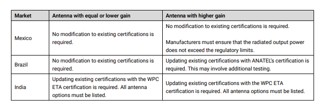
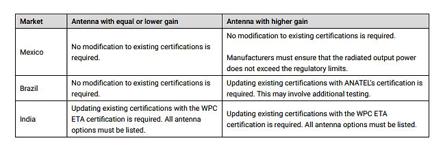
Market | Antenna with equal or lower gain | Antenna with higher gain
Mexico | No modification to existing certifications is required. | No modification to existing certifications is required. Manufacturers must ensure that the radiated
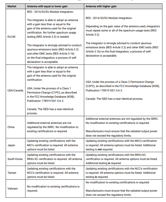
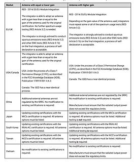
Market | Antenna with equal or lower gain | Antenna with higher gain
EU/UK | RED - 2014/53/EU Module Integration: The integrator is able to adopt an antenna with a gain less than or equal to the gain of the antenna used for the original
/1005010466566322.html Das ist ein ST32H7R3, der läuft mit 600MHz und hat vor allen Dingen USB HIGH Speed im Chip. Und einen 16Bit Bus bis 50MHz. Da habe ich ein Board hier aber auch noch nichts damit gemacht. Ist leider nur ein Blink Demo drauf ohne USB.
Noch ist nichts dafür geschrieben, ich bin gespannt. Ich habe mir vorgenommen mit Cube-IDE aber LowLevel auf Registerebene ohne HAL zu arbeiten. Leider hänge ich immer noch an der RCC-Konfig und bekomme meinen Wunschtakt nicht hin. Diese H7 sind schon etwas tricky...
DS1220Y 6. If the CE low transition occurs simultaneously with or later than theWE low transition in write cycle 1, the output buffers remain in a high impedance state during this period. 7. If the CE high transition occurs prior to or simultaneously with thWE high transition, the output buffers remain in a high impedance state during this period. 8. If WE is low or theWE low transition occurs prior to or simultaneously with CEe low transition, the output buffers
Min Max Min Max Min Max t WRITE cycle time 70 150 200 ns AVAV tAVWL Address valid to WRITE enable low 0 0 0 ns tAVEL Address valid to chip enable 1 low 0 0 0 ns WLWH WRITE enable pulse width 50 90 120 ns tELEH Chip enable low to chip enable 1 high 55 90 120 ns WHAX WRITE enable high to address transition
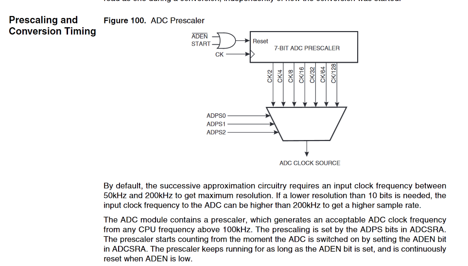
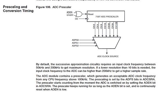
circuitry requires an input clock frequency between 50kHz and 200kHz to get maximum resolution. If a lower resolution than 10 bits is needed, the input clock frequency to the ADC can be higher than 200kHz to get a higher sample rate.
The ADC module contains a prescaler, which generates an acceptable ADC
Schaltnetzteilen. Kann ich es im ausgebauten Zustand einschalten? Und wenn ja, wie. Pin 8 auf LOW/HIGH (Spannung? 3,3V ,5V ...) Grüße, Werner PS: Ich habe im Internet bezüglich dieses Netzteils nichts gefunden.
sbi PORTC, 0 ;PWM2 mit Port C0 sbi PORTD, 4 ;PWM3 mit Port D4 cbi PORTD, 5 ;PWM4 mit Port D5 ldi AL, LOW (51200) ;0xC800 sts Motb, AL ldi AL, HIGH (51200) sts Motb+1, AL clr AL sts Motb+2, AL ldi AL, LOW (512) ;Schritte/U durch 100 für Winkelberechnung sts Moth, AL ldi AL, HIGH (512) ;Schritte/U durch
time of rainy weather From the classroom to the 2 cafeteria, the fox you campus 1.8 million to read. High efficiency: 83% (typical), sufficient 60 years old, fat East founder in 3 the east, announced the Spring Using solar cells 320,000 Reading Guo Shiqiang reiterated the Less peripherals: only one inductor selection criteria of the 53 million Reading Low-voltage battery protection function The input current can be adjusted by the inductance Sohu Scope of application What is the history and Funny n… culture of Wuxi County and the famous people? Solar
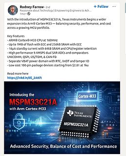
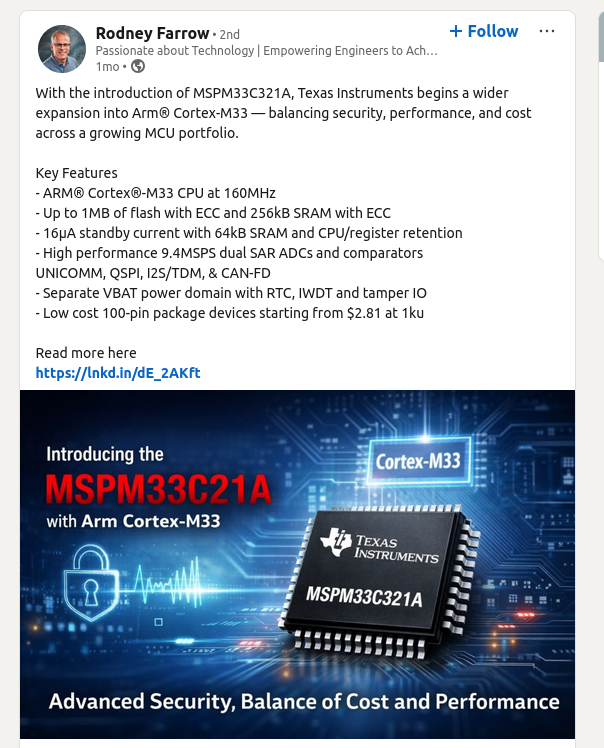
with ECC and 256kB SRAM with ECC
- 16µA standby current with 64kB SRAM and CPU/register retention
- High performance 9.4MSPS dual SAR ADCs and comparators
UNICOMM, QSPI, I2S/TDM, & CAN-FD
- Separate VBAT power domain with RTC, IWDT and tamper IO
- Low cost 100-pin package devices starting from $2.81 at
Einen wakeup-Puls (200 µs low) hast Du vor der Abfrage gesendet? Die Dinger sind darauf trainiert, sich energiesparend zu verhalten. Daher kann es gut sein, dass sie jeden anderen Traffic auf dem Bus erstmal ignorieren.
Power-MOSFET, 100 V CanPAK MN G Features D • Pb-free plating; RoHS compliant • Dual sided cooling • Low profile (<0.7 mm) • Excellent gate charge xDS(on)product (FOM) • Very low on-resistance DS(on) S • Optimized for high switching frequency DC/DC converter S D • Low parasitic inductance • Halogen-free

 Bild
Bild
 Bild
Bild
 Bild
Bild
 Bild
Bild
 Bild
Bild
 Bild
Bild
 Bild
Bild
 Bild
Bild