-
Thread
Fehler zum nachbauen :-)
Seek-Thermal-Compact-Imaging-Camera-iPhone-iOS-Infrared-Heat-Sensor-Night-Vision/263416225905?epid=2255628542&hash=item3d54d4a071:g:~roAAOSwB4BaS-vb
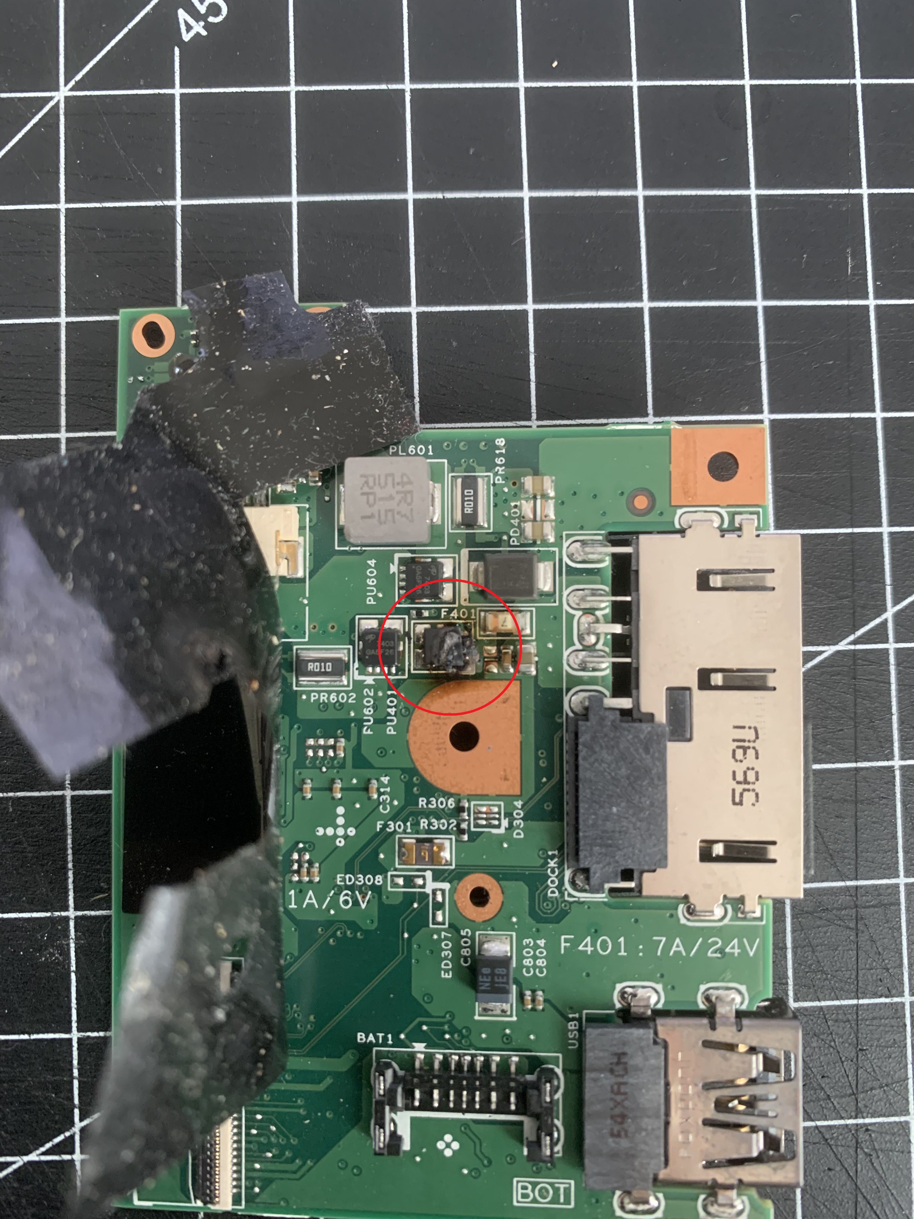
nicht lustig. Habe mir eine China Platine gekauft diese kam gestern auch darauf waren 5 Sicherungen a 5A mt 20x5 so weit ok nur brauchte ich 8A. also andere Sicherung verbaut. Dabei fiel mir der dicke Draht in der alten 5A Sicherung auf und ich wollte wissen, ob die auch wirklich bei 5A trennen.
-
Thread
LTspice OpAmp Radio Simulation
Gleichrichtereffekt Die Signale in der Simu sind sehr klein. Das 1mV an R2 führt zu Strömen im sub-µA Bereich. Das läuft immer noch über die Kapazität und "Leckströme" der Dioden, ohne dass der zweite OPV seinen Ausgang um eine Diodenspannung springen lassen müsste. Wenn das Signal vor der Gleichrichterstufe
der > begrenzten GBW bzw. Slewrate des OPV Mit den Bauelementen OPV *LT1028* und Schottkydiode *BAT54* simuliert bringt gute Werte. Größere Ausgangspannung und Gleichrichtung
-
Thread
Ostern- Vielleicht mal wieder Detektorempfänger ? Gesperrt
e88cc-tube-PAIR-d-getter-6922-CCA-CV2492-pinched-waist-GOLD-valve-preamp-valvo/254823657678?hash=item3b54ac70ce:g:B98AAOSwzmZf8G5W https://www.ebay.de/sch/m.html?_odkw=&_ssn=wege_high_tubes&hash=item3b0ef536a3%3Ag%3AgXAAAOSwkWNZmHSG&item=253654021795&_osacat=0&_from=R40&_trksid=p2046732.m570.l1313&_nkw
Mini-Fundus eine passende Röhre gefunden, aber sie steht nicht in der RTT von 1968. Die Bezeichnung ist A411, das ist mittig gedruckt, da fehlt nichts davor oder dahinter. Lt. Tabelle gibt es aber nur A415=A408=RE084, A409=RE074, A4110=REN904.
-
Thread
Checksumme im Funkprotokoll von Thermo_Hygro-Sensor
. Jedes Mal ein Reset - ich wollte gleiche Werte bekommen. Dann 2x 2gleiche Werte. [code] low-Bat?;Temp HH.H;99% 11 1110 0101 1001 1011 0111 0000 1011 1100 11 1101 1101 0 1101 0 0010 1001 1001 0001 0111 1101 1111 1001 1100 1110 ---------------- 21.9°C;54% 11 1110 0100
Ohne Parity, in Bitreihenfolge 1111 1001 0 F9 1101 0101 1 D5 0111 0011 1 73 0111 1010 1 7A 1010 0110 0 A6 1000 0011 1 83 1010 0010 1 A2 1100 1111 0 CF 1001 0100 1011 1001 94B9 z.B also: F9D5737AA683A2CF94B9 Parameters: polynom : 0x8689 order :
-
Thread
20Euro Embedded System mit ARM, 128MB ram und 256MB Flash
wlan0: STA 00:22:fb:93:66:a8 RADIUS: starting accounting session 4C83F3A3-0000001
Jedoch weiß ich im Moment nicht, was ich für eine Batterie verwenden soll. Der Spannungsabfall am BAT54 wird wohl 0,5V sein. Mit 2x 1,2V = 2,4V - 0,5V = 1,9V sollte ich wohl hinkommen. Nur habe ich gerade keinen Halter dafür zur Hand.
-
Thread
Pollin MOTOROLA VIP1710
signiert. Der Kernel Public RSA-Key lautet: Modul: 0xffffffff65b0e4da4f5bc26c97677ddde52f71c7a2f8a38d58011384ff319811d1022965ebecfbefbf205e7d15c1c08318f0dda0670ba4ddda360d8785cfc2160402dcbd02732b9f51b59df46576089700b61573838561fc2c2a857bbf7247995d44a4ed534080dc6af1f582f8d8267e54fb0ee5b982e014c4d855a8c734a9df
v1.4 - External heatsink - with flash So only 2 out of 5 with flash :-( Now for streaming from a Dreambox 7000-S , MPEG-TS. Should i start with the ones with flash or those without ? I have an Ubuntu Server with TFTP & Apache. And I am currently running DHCP from a WRT54G (DD-WRT). Where
-
Thread
Minutengenaue 24 Stunden-Wortuhr - wer will mitbauen?
Link zum Zipfile https://rawgit.com/code-creator/wordclock2scrnv/master/WordClock2.zip SHA-1 0ae4bc0192d96df5df6ae16e618521113e2cf6cc wordclock2.exe SHA-256: F814A93E5E3949184226BB86D37CFD7AE4F247EB93EC81994398D02621F989AA Virengeprüft bei Virustotal.com mit 0/54.
Hier noch der Debug-Output: [c] sending: 'AT+CWJAP?<0d>' AT+CWJAP?<0d><0d><0a>+CWJAP:"fm7170"<0d><0a><0d><0a>OK<0d><0a> sending: 'AT+CIFSR<0d>' AT+CIFSR<0d><0d><0a>192.168.10.119<0d><0a> sending: 'AT+CIPMUX=0<0d>' AT+CIPMUX=0<0d><0d><0a><0d><0a>OK<0d><0a> sending: 'AT+CIPSTART
-
Artikel
Standardbauelemente
Sperrspannung, trr<50ns bzw 75ns 3A, 50..1000V R D BAT46 0,10 Kleinsignal-Schottky-Diode 150mA D,R D BAT54(A/C/S) 0,04 sehr schnelle Kleinsignal-(Doppel-)Schottky-Diode 200mA R,D,I D SB120..SB160 0,13 Schottky-Diode 1A 20-60V R,I D 1N5817
=40mA, Quad: TS914 PDF alle 0,80 LMC6484 4 1,5 0,9 3 2 pA 4 pA Vcc+0,2V Vee-0,2V over the rail Vcc-0,2V Vee+0,2V @2kΩ 5V 3 Iout=16mA@5V Iout=28mA@15V PDF R 2,35 OPA2340 2 5,5 6 0,150 1 pA 1 pA Vcc+0,5V Vee
-
 Bild
Bild
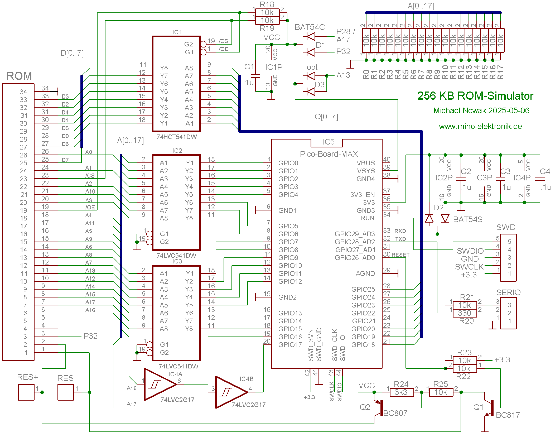
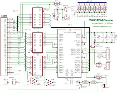
Schaltplan eines Pico-Board-MAX ROM-Simulators
GPIO23 GPIO24 GPIO25 GPIO26 GPIO27 GPIO28 GPIO29 GPIO30 GPIO31 GPIO32 SWDIO GND SWCLK GND RESET SWD BAT54S C1 1u C2 1u C3 1u C4 1u R21 10k R20 330 R23 10k R22 10k R24 3k Q1 BC807 Q2 BC807 IC4A 74LVC2G17 IC4B 74LVC2G17 IC3 74LVC541DW IC2 74LVC541DW IC4A A17 A16 A15 A14 A13 A12 A11 A10 A9 A8 A7 A6 A5 A4 A3 A2 A1 G2 G1 G1 G2 P32 RES+ RES- +3.3
-
Thread
Epidemiologischer Verlauf und Analyse von Krankheiten Gesperrt
/wissenschaft/medizin/neues-coronavirus-welche-menschen-durch-covid-2019-besonders-gefaehrdet-sind-a-261c0cf4-2ca3-4a42-a85b-d3dc546faa98
@ A.K. (PRX) Danke! Namaste
-
Thread
Mini-Farbdisplay (+mehr) für 1 Euro
dasmx -a -c65c02 miuchizflash.bin
,0,127,73,73,73,54 , 0,62,65,65,65,34" ...oder sollte man besser DATA benutzen: ======================================== DATA 0,126,17,17,17,126 'A DATA 0,127,73,73,73,54 'B DATA 0,62,65,65,65,34 'C DATA 0,127,65,65,65,62
-
Thread
Datenblatt IE 500 (DBM)
in meinen alten Akten auch nichts gefunden. Was man im Net findet ist, dass IE500, MD108, SBL1 u.v.a.m. immer in den gleichen Topf geworfen werden. Das gibt es ja heute noch: http://www.amidon.de/contents/de/d188.html Zu IE in Frankfurt meine ich mich zu erinnern, dass das nur ein Vertrieb war
MHz-Konverter mit normalen 1N4148 [1]. Doppel-Schottky-Dioden im SOT23 gibts auch zu Genüge, z.B. BAT54. Wenn du einen besonders niedrigen Frequenzbereich haben willst, kannst du hier bequem mit verschiedenen Kernmaterialien und Windungszahlen experimentieren. Beste Grüße, Marek [1] TenTec-Kit
-
 Bild
Bild
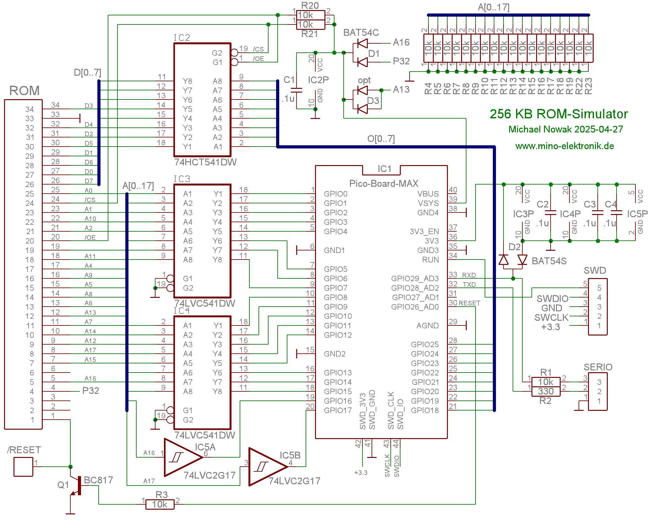
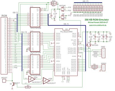
Schaltplan Pico-BOARD-MAX mit ROM und Logikbausteinen
R20 10k, R21 10k, BAT54C, D1, P32, A[0..17], IC2, 256 KB ROM, Michael Nowak 2025-04-27, www.mino-elektronik.de, IC1, Pico-BOARD-MAX, VBUS, 3V3, GND4, 3V3_EN, 3V3, GND4, R4 bis R22 10k, IC3, 74HCT541DW, D[0..7], A[0..17], IC5A, 74LVC541DW, IC5B, 74LVC2G17, IC5C, 74LVC2G17, SWDIO, SWCLK, GND, +3.3, SWD_DIO, SWD_CLK, SWD_GND, SERIO, R1 10k, R2 330, Q1 BC817, R3 10k
-
 Bild
Bild
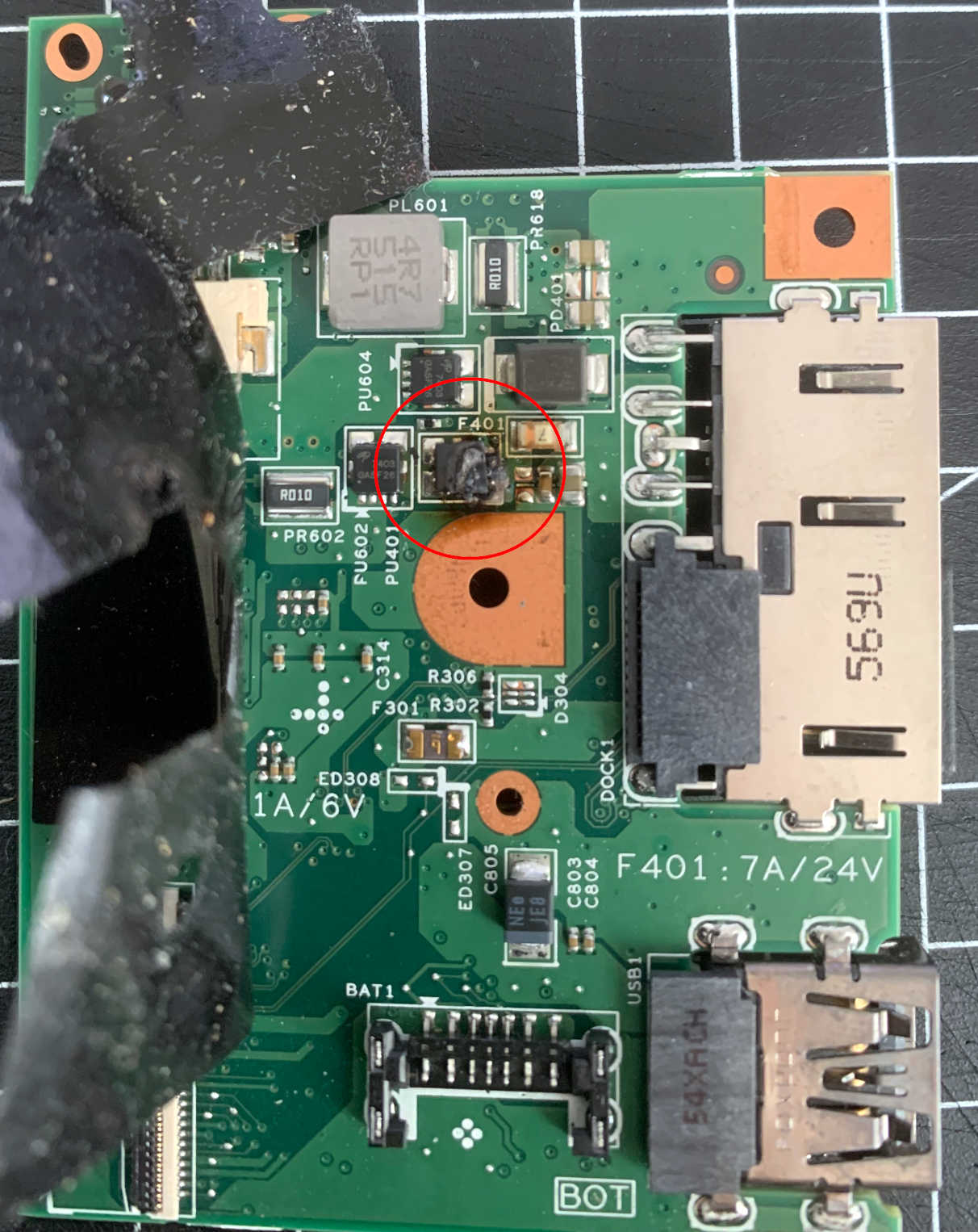
Nahaufnahme einer beschädigten Leiterplatte mit Brandspuren
PL601 PR618 R5P1 R010 PD401 PU604 F401 R010 PR602 PU401 C314 R306 F301 R302 D304 ED308 DOCK1 1A/6V C805 ED307 C803 C804 USB1 F401:7A/24V BAT1 USB1 54XACH BOT
-
 Bild
Bild
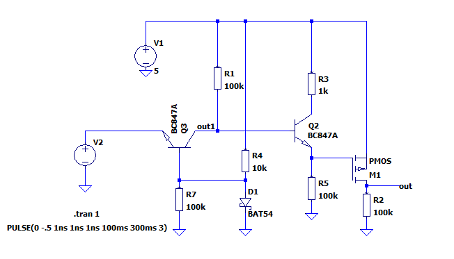
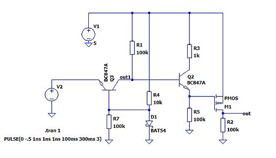
Schaltplan einer Transistorschaltung
V1 5 R1 100k Q3 BC477A out1 R4 10k V2 Q2 BC847A R3 1k D1 BAT54 R7 100k R5 100k M1 PMOS R2 100k out .tran 1 PULSE(0 -0.5 1ns 1ns 100ms 300ms 3)
-
Thread
Anforderungssammlung CAN Hausbus mit PIC µC
einen, der die Anforderungen erfüllt. - Schaltregler und Befilterung hinzu - Referenz-Diode für A/D hinzu. - Frei gewordene Pins auf Stiftleisten legen. Villeicht ändere ich die Stiftleisten auf SMD, der RM 2,54 soll aber bleiben. Dadurch wird das Modul universeller, der Einbau in meine
einfachen Layouts....... Kein Schaltregler, bei so wenig Strom, finde ich, ist es unnötig. Bißchen BAT54S und ....Watchdog sei dank, es geht. Gruß Helmut
-
Artikel
Compact Plus Blutzuckermessgerät-Hardware
(TFDU2201) Buzzer Piezo Schallwandler D1 BAT54W T2 ZXTN23015CFH (NPN) XTAL1 32 Khz XTAL2 4 Mhz Pinbelegung Mega168. Wie oben mittles Messungen ermittelt. Ohne Garantie auf Vollständigkeit und Richtigkeit. Pin Port Funktionen Verwendung 1 PD3 (
/OC0B/T1) VCC enable (12 V step-up) 10 PD6 (PCINT22/OC0A/AIN0) frei 11 PD7 (PCINT23/AIN1) direkt an Batteriespannung 12 PB0 (PCINT0/CLKO/ICP1) an Transistor T1 (schaltet 12 V über 100Ω gegen GND als Grundlast bzw. zum Entladen) 13 PB1 (PCINT1/OC1A) Display
-
Thread
Projekt : GPS Tracker
Y•ŒŽ|" "000000070 8C 8C 8E CC 0A C4 B9 BE-08 8A 88 88 4C 8A 4A 4C |ŒŒŽÌ.Ĺ¾ ŠˆˆLŠJL|" "000000080 8C 8C 8A 0C 8A 48 88 0C-8C 88 0C 0A 8C 08 0C 8A |ŒŒŠ ŠHˆ Œˆ .Œ Š|" "000000090 88 8A 4E 88 28 F3 77 49-49 49 2A 6A 59 4C 8A 8C
,,25,03,273,*78 $GPGSV,4,4,13,19,50,296,42*4D $GPGLL,4959.54084,N,00854.61071,E,162954.00,A,A*60 $GPZDA,162954.00,27,10,2008,00,00*65 $GPRMC,162955.00,A,4959.53980,N,00854.60471,E,10.994,272.74,271008,,,A*54 $GPVTG,272.74,T,,M,10.994,N,20.373,K,A*39 $GPGGA,162955.00,4959.53980,N,00854.60471
-
Thread
Beispielprogramm für RFM12 433MHz Funk-Module
uart_puts("Falsch!"); } } [/c] Das Ergebniss ist: [c] S e n d e r l a e u f t ! \n F a l s c h ! F a l s c h ! F a l s c h ! F a l s c h ! F a l s c h ! F a l s c h ! F a l s c h ! F a l s c h ! F a l s c h ! F a l s c h ! F a l s c h ! F a l s c h ! F a l s c h ! F a l s c h ! F a l s c h ! F a l s c h ! F a l s c h ! F a l s c h ! F a l s c h ! F a l s c h ! F a l s c h ! F a l s c h ! F a l s c h ! F a l s c h ! F a l s c h ! F a l s c h ! F a l s c h ! F
-
Thread
AX81 - ZX81 im AVR
m.ebay.co.uk/itm/Sinclair-ZX80-ZX81-Spectrum-16k-Jupiter-Ace-Emulator-PCB-AX80-/182657572231?hash=item2a873d5d87%3Ag%3AKRgAAOSwuq9ZYK~R&_trkparms=pageci%253Afd149a91-6534-11e7-b753-74dbd18045fb%257Cparentrq%253A2b15225015d0abd99a0e4813ffed08a7%257Ciid%253A7 Their going fast. Only 5 left.
Picture of board nearing completion. A few errors have been noted. Keyboard connector pin 5 has no track to the atmega, due to typo on schematic. The two keyboard connectors are not at the correct spacing, out by 2.54mm as they overlap,
-
Thread
Speedport W700V Call & Surf Comfort/T-ISDN ???
anschaffen und wenn ja eher direkt am W700V oder am NTBA anschließen. Danke für einen Tip! Gruß A. S.
Haaren herbeigezogen; eine andere (an ebenfalls recht langen Haaren herbeigezogene) Variante wäre: A feiert krank, ist aber bei seiner Freundin B. Beim Anruf in seiner Firma möchte A natürlich nicht, daß die Rufnummer seiner Freundin übermittelt wird ...
-
Artikel
Xilinx USB-JTAG-Adapter
SMD0805 1 R14 360 SMD0805 4 R27, R28, R29, R55 2,2K SMD0805 23 R1-R12, R26, R30, R31, R47, R48, R53, R54, R58, R59, R64, R65 10K SMD0805 1 R46 15K SMD0805 13 R13, R16, R33, R35, R36, R38, R39, R41, R42, R50, R56, R57, R63 20K SMD0805 1 R62 47,5K oder 200K** SMD0805 1 R61 64,9K oder 270K** SMD0805 2 R45,
TPS71718DCK SC70-5L 1 IC13 MCP1825S-33 oder MIC2920A-3.3V SOT223 * Je nach Verfügbarkeit bestücken. Falls bestückt können mehrere JTAG-Kabel gleichzeitig benutzt werden. + Rest Menge Bauteil Wert Größe 1 D1 1SMA5915BT3G SMB 2 D2, D3 BAT54 SOD323-W 1 D4
-
 Bild
Bild
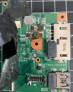
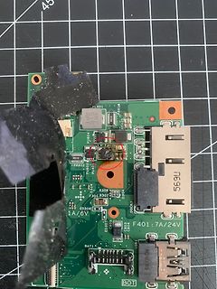
Foto einer beschädigten Leiterplatte mit Brandspuren
BAT1 ED307 C805 C803 F401 7A/24V USB1 54XACH DOCK1 569U ED308 C314 R301 FU602 PU401 PU604 R51 PR601 R401 R304 D304 R10 PD401 PX618 DL601
-
Thread
AIS-Position von der Ostsee, aber werbefrei
geschichte/buckelwal-in-der-ostsee-warum-fuer-unsere-vorfahren-die-party-begann-wenn-ein-wal-strandete-a-75f4056a-7cc9-4669-9f0f-782fcea016cf
nicht über die Rettung, sondern um die Kadaver." https://cdn.prod.www.spiegel.de/images/187d90e5-4a8d-41e3-8dc5-c9372e0ab486_w960_r1.5_fpx24.35_fpy54.99.webp Was sollen die beiden Röhren auf dem Kopf darstellen?