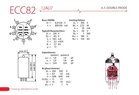
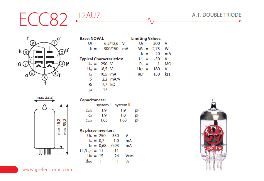
ECC82 12AU7 A. F. DOUBLE TRIODE Base: NOVAL Uf = 6,3/12,6 V If = 300/150 mA Limiting Values: Ua = 300 V Wa = 2,75 W Ik = 20 mA Typical Characteristics: Ug = -50 V Rg = 1 MΩ Ia = 10,5 mA S = 2,2 mA/V Ri = 7,7 kΩ μ = 17 Ua = 250 V Ug = -
power transistor BD330 FEATURES PINNING • High current (max. 3 A) PIN DESCRIPTION • Low voltage (max. 20 V). 1 emitter 2 collector, connected to metal part of APPLICATIONS mounting surface 3 base • Powerswitchingandamplification,especiallyinportable equipment or e.g. car radio output stages. DESCRIPTION
) and symbol. QUICK REFERENCE DATA SYMBOL PARAMETER CONDITIONS MIN. TYP. MAX. UNIT VCBO collector-base voltage open emitter − − 32 V VCEO collector-emitter voltage open base − − 20 V CM peak collector current − − 3 A P total power dissipation T ≤ 45 °C − − 15 W tot mb hFE DC current gain IC= 0.5 A; CE
Philips_IC02a_Video.pdf Aber der TS9347 macht wohl das endgültige Videosignal. Vielleicht ist es ein normgerechtes BAS mit 50 Hz Halbbildfrequenz, 312,5 Zeilen pro Halbbild sieht gut aus.
eingespeisten Videosignal, die sollen nicht aus den Grafikcontrollern > kommen. Aus dem TS9347 kommt doch BAS, also Luminanz + Composite Sync. Solange der Monitor nicht unnötigerweise noch separat HSync und VSync bekommt, sollte es also reichen, dahinter aufzutrennen und das externe (F)BAS-Signal einzuspeisen
Continue with item 6.5. – Check that CH II variable gain knob is set to CAL. positi- on. – Set time base to 0.5 ms/div. 6.5 CH II 20 mV/div (3% accuracy) – Press CH I/II pushbutton (IN position) to select channel II. – Set attenuator CH II to 20 mV/div. – Connect a 100 mV pp (accuracy ± 0.1%), 1 kHz square
die Größe mit Beinchen betrachten, schließlich nehmen > auch die Platz auf der Platine weg. Der BAS4002A mit SOT143 ist da unschlagbar, mit Beinchen 2,9x2,4 mm
Primary lithium battery LSH 20 3.6 V Primary lithium-thionyl chloride (Li-SOCl ) 2 High power D-size spiral cell Benefits ● High voltage response, stable during Cell size references UM1 – R20 – D most of the lifetime of the application
geht nicht, Herr Dr. Mandelbrotmenge? Ca. 1984: GFA Basic für DOS. Ein Beispielprogramm: MANDEL.BAS, im Kopf mit "MANDELBROT" betitelt.
Bei 6, spätestens sieben ist es dann aber deutlich "mandelbrotig". Ob erste Spuren von Chaos bei 20 oder 30 losgehen, darüber mag man auch wieder vortrefflich streiten können.
RATINGS (Ta = 25°C) CHARACTERISTIC SYMBOL RATING UNIT Collector−Emitter Voltage V 25 V CEO Collector−Base Voltage V 35 V CBO Collector Current I 150 mA / ch C Input Voltage VIN(Note 1) 20 V Input Current IIN(Note 2) 10 mA Power Dissipation PD(Note 3) 0.75 W Operating Temperature Topr −40~85 °C Storage Temperature
Die Firma Exicon hat MOSFETs für den Linearbetrieb im Angebot. Ein Beispiel wäre z.B. der ECX10N20 im TO-247 Gehäuse.
wäre das optimal gewesen. Hier auf der Seite ganz unten: https://jlcpcb.com/quote/pcbOrderFaq/Base%20Material Ich hatte überlegt das auszuprobieren, aber die Erklärung, wie man solche Inseln definieren muss, war mir schon nicht klar. Und es hätte auch mehr gekosten. Frank O. schrieb im Beitrag
Stable Region 0.1 mF U T SR T 40 - 2.0 O E O T 1 ,t U Unstable Region for 0.1 mF capacitor only Vo20 - 4.0 T LP2951CN O 0.1 Lower unstable region is for 0.1 mF only. 0 - 6.0 1 mF and 100 mF show no instability with low ESR values. 0 5.0 10 15 20 25 30 35 40 0.01 0 10 20 30 40 50 60 70 80 90 100 Vin
from embedded files -ext[+] EXT (-extension) Process files with specified extension -F[OFFSET] (-fixBase) Fix the base for maker notes offsets -fast[NUM] Increase speed when extracting metadata -fileOrder[NUM] [-]TAG Set file processing order -i DIR (-ignore) Ignore specified directory name -if[NUM] EXPR
Ok, ich schaue mir mal die Datenblätter dazu an. Bestellen wäre bequemer gewesen ;-) Habe so an die 20 verschiedene 6-Beiner da.
ohne Signal, so ist der Opto aktiv. Der zweite Pfad sind Kondensatoren von TTL-Signal direkt auf die Basen der Transistoren im HV-Teil. Je nach Geschwindigkeit des Fehlers kann man den Zweig identifizieren.
6. ID Definitions Command Type MX25L12835F RDID 9Fh Manufacturer ID Memory type Memory density C2 20 18 Electronic ID RES ABh 17 REMS 90h Manufacturer ID Device ID C2 17 Manufacturer ID Memory type Memory density QPIID AFh C2 20 18 P/N: PM1795 Rev. 1.6, July 22, 2016 26 M X 2 5 L 1 2 8 3 5 F 9-7. Read
During voltage transitions, all pins may overshoot Vss to -2.0V and Vcc to +2.0V for periods up to 20ns, see the figures below. Figure 44. Maximum Negative Overshoot Waveform Figure 45. Maximum Positive Overshoot Waveform 20ns 20ns 20ns Vss Vcc + 2.0V Vss-2.0V Vcc 20ns 20ns 20ns 12-2. CAPACITANCE TA
During voltage transitions, all pins may overshoot Vss to -2.0V and Vcc to +2.0V for periods up to 20ns, see Figure 4, 5. Figure 4.Maximum Negative Overshoot Waveform Figure 5. Maximum Positive Overshoot Waveform 20ns 20ns 20ns Vss Vcc + 2.0V Vss - 2.0V 20ns Vcc 20ns 20ns CAPACITANCE TA = 25 C, f =°1.0
Updated and revised the technical content. No changes to the meaning, language, or formatting of the 5/20/2014 5.0 None technical content. 6/30/2015 6.0 Major Significantly changed the technical content. 10/16/2015 7.0 Major Significantly changed the technical content. 5/10/2016 8.0 Major Significantly changed
Generatorausgangs bestimmt. Wie hoch soll der Basisstrom denn werden? Laut Dablamaximal 100 mA Base Current IB 0.1 Ad https://www.onsemi.com/download/data-sheet/pdf/bd676-d.pdf ciao gustav
zur Erkennung der Bewegungsrichtung), der kostet ungefähr 10-mal so viel, wie ein 1-kanaliger, also 20 - 30€. Natürlich darf sich nichts Nennenswertes im Erfassungsbereich ändern, weil das als Objekt erkannt werden würde. Das schränkt die Einsatzmöglichkeiten ein.
operating area. Because allowable MOSFET SOA current falls off at high drain-to-source voltages, the 20V avalanche diode D6, in conjunction with R9, R11, and Q3 provides extra current into the timer network when the IN-to-OUT voltage exceeds 20V plus Q3’s base-emitter volt- age. The 4.7V avalanche diode
click “OK”. 7. Click your mouse inside the Filename: box and edit the filename. This will be the base filename for all of the Gerber files. Remember this name as you will need it when generating the drill files. I recommend placing a version number and a date in the filename for reference. 18 8. Check
Es sind +/- 12V, also (mit 2V Restspannung pro Darlington) 20Vpp = 7.07Veff entsprechend ~16W an 3Ohm. Deine 6W stimmen bei unipolarer Betriebsspannung.
> Es sind +/- 12V, also (mit 2V Restspannung pro Darlington) > 20Vpp = 7.07Veff entsprechend ~16W an 3Ohm. > Deine 6W stimmen bei unipolarer > Betriebsspannung. Stimmt, habe ich übersehen. - Deswegen ein "Like" von mir.
SCON.2; // timer2 run enable C_T2 : sbit absolute SCON.1; // timer2 clock source selection: 0=timer base internal clock, 1=external edge counter base T2 falling edge CP_RL2 : sbit absolute SCON.0; // timer2 function selection (force 0 if RCLK=1 or TCLK=1): 0=timer and auto reload if count overflow or T2EX
schlechten Verkabelung geschuldet. Nicht ohne Grund wurde auch die Anschlußleitung Western-Western der Basen deutlich gekürzt. Da reichte schon ein knapper Meter, dass die Basen nicht mehr stabil synchronisieren. > Dafür war die OpenCom Serie um so besser.:) Leider inkompatibel, nannte sich "DECT 2"
Verkabelung geschuldet. > > Nicht ohne Grund wurde auch die Anschlußleitung Western-Western der > Basen deutlich gekürzt. Da reichte schon ein knapper Meter, dass die > Basen nicht mehr stabil synchronisieren. Das Szenario ist denn wie alt bitte, u. mit welcher Schnittstellentechnik zur Basis von
released. 2. This clock should be switched after the PLL clock oscillation is fully stabilized. Figure 7.20 State Transition When Using the On-chip Oscillator Clock R01UH0220EJ0120 Rev.1.20 Page 127 of 642 Sep 10, 2013 R32C/152 Group 7. Clock Generator 7.7.2 Wait Mode The base clock stops in wait mode, so
Phase Phase 60 0 pF 80 60 80 0 pF 50 60 50 60 100 pF 1000 pF 100 pF 40 40 P 40 P a 40 a s s d30 500 pF 20 M B30 500 pF 20 M − 1000 pF a d Gain a n20 0 g −20 0 g a n a n G Gain − G − 10 −20 e 10 −20 e g g 0 Vs = 5.0 V −40 0 Vs = 5.0 V 0 pF −40 RL= 600 Ω 100 pF 500 pF RL= 100 kΩ −10 0 pF −60 −10 CL= 0 pF 100
Ich hatte früher (als ich noch aktiv war) bei größeren Schaltungen (auch gelegentlich mehr als 20 Seiten) eigene Subsheets für die Versorgungspins der ICs. Es kommen halt noch ein paar Seiten hinzu - PDF(-Papier) ist geduldig 😀. Entweder man muss bei Fehlern in der Versorgung suchen, dann hat man
transistors (BJTs). In BJT technology, the collector is one of the main terminals (the others being the base and emitter). Over time, however, VCC has become a more general term used to denote the positive power supply voltage in circuits, regardless of whether they use BJTs or not. VDD: This term stands
. Ambient temperature at running —— 0~40°C (32~104 °F) Temperature at storage —— -20~55°C (-4~131 °F) 0 Temperature at tranportation —— -20~60°C (-4~140 °F) o O Air Humidity O At running —— 5%~85%, no condensationor freezing At storage — 5%~95% o www sakohzcom/ 04 Chapter 3 Installation
e 4 O 9 a 3 ) G o 6 S 2 D V R 3 1 0 0 0 2 4 6 8 10 12 14 16 18 20 0 3 6 9 12 15 Q - Gate Charge (nC) VGS - Gate-to- Source Voltage (V) G001 g G001 1 An IMPORTANT NOTICE at the end of this data sheet addresses availability, warranty, changes, use in safety-critical
Genau da sitzt das Problem, Weil >10x der Impulsstrom zum Laden des Elkos (jeweils 2...8µF, 10...20Ω) vor dem Wandler den Schalter ganz schnell verschleisst, sofern es kein Kondensatornetzteil ist. Zweitens entsteht durch den Einschaltstromimpuls ein Überschwinger. Bei geeigneter Anordung klappt
Herstellers das Verhältnis Einschaltstrom zu Nennstrom weit variieren. Bei den von mir oben verlinkten LED BASE CLASSIC A von Osram/LEDVANCE liegt der Einschaltstrom bei der 8,5W Version, die etwa einer 60W Glühlampe entspricht, bei 7,5A. Bei etwas mehr als der doppelten Leistungsaufnahme als der 4W LED ist der
getan. Selbst günstige 0815 Consumerware unter den ADC sind heute oft viel bessser als das was vor 20 Jahren bei State Of the Art Messtechnik verbaut wurde. Zudem haben sich auch die Möglichkeiten der Digitalen Signalverarbeitung enorm weiterentwickelt. Das macht ja z.B. diesen Wahnsinnigen Preisverfall
minutes under the specified operation temperature. Temperature Range: Operating 0℃ to +50℃ Time Base Accuracy: ±1.5 ppm ± 1 ppm/year[/pre]
Typprüfung ... der hier: https://colorcomputerarchive.com/repo/Documents/Manuals/Programming/Introl-C%20Compiler%20Reference%20Manual.pdf). *) das hier: https://www.cs.otago.ac.nz/homepages/andrew/poly/OmegasoftPascal.pdf
spart die Ressourcen auf Deinem µC ein, die für die Erzeugung des BAS-Signals benötigt werden.
counter within the >current psect. This means that the addresses set with ORG are relative to >the base address of the psect, which is not determined until link time. > >Note: The much-abused ORG directive does not move the location counter to >the absolute address you specify.
Eproms, die Anfang der 90er mit 'intelligenten' Algorithmen gebrannt wurden, sind oft nach 20 Jahren schon nicht mehr komplett lesbar (hier schon öfter aufgeschlagen). Also, lesbar schon, aber es steht Grütz drin. Wenn, dann brennt man so einen Stein also mit dem sturen 50ms per Byte Algorithmus
garantiert so lange hält. Alternativ könnte man die Daten auf ein Blatt Papier drucken. Vorne base64 codiert (das wird man in 18 Jahren mit Sicherheit erkennen und lesen können) und hinten als QR Code, um eine Alternative zu haben.
wandler angeschlossen und gescannt. Ist 250kbaud seriell. Bild 1 oberer kanal das kommt alle 20ms, keine daten drin. unterer kanal sind offenbar RX und TX gemischt. Wie unterscheide ich was RX und was TX ist? Bild 2 Das sind daten zwischen dan 20ms sync. Dann habe ich einen seriell-usb
ganz gut. Das macht immerhin 30W Unterschied. Ist aber schon komisch, dass deine Daly-Anzeige bei 20A Ladestrom peaks bis 40A misst.
data set-up time 250 - 100 [5] - 50 - ns n SU;DAT R o tr rise time of both SDA and SCL signals - 1000 20 300 - 120 ns e e . n tf fall time of both SDA and SCL - 300 20 × 300 20 × 120 [8] ns 6 i [3][6][7][8] [9] — o signals (VDD / 5.5 V) (VDD / 5.5 V) 4 m t set-up time for STOP condition 4.0 - 0.6 - 0.26
memory and could check for data in a particular handle name's expanded memory pages. Use Function 20 (Set Handle Name subfunction) to assign a handle name to an EMM handle or Function 21 (Search for Named Handle subfunction) to obtain the EMM handle associated with the handle name. In addition, you
SrcHandle, SrcSegment, SrcOffset, DstHandle, DstSegment, DstOffset) 'Copies memory from EMS or base memory to EMS or base memory, where: ' 'Length& = Length of memory to copy in bytes 'SrcHandle = EMS handle of source memory (use 0 if source is base memory) 'SrcSegment = Segment of
Offset of source memory 'DstHandle = EMS handle of destination memory (use 0 if destination is base memory) 'DstSegment = Segment of destination memory (or page number if destination is EMS) 'DstOffset = Offset of destination memory 'Determine the source and destination memory types by

 Bild
Bild