-
PDF
nokia_6085_rm-198_service_schematics_v2.pdf
Gnd ACITx GENIO41 42 GENIO40 10n { GENIO42 Y15 41 GENIO41 10 UI MR SENSOR DIG_AUDIO(5:0) 1 W8 EarDataL GENIO43 AA15 43 } 1.8V: flip open GND GND 2 Y8 EarDataR GENIO44 R14 44 68 GENIO68 CAM_CLK 0 CAM_CTRL_CMT(4:0) 3 Y9 MicData GENIO45 V14 45 53 GENIO53 CAM_ENABLE (xshutdown) 1 0 R10 W14 46 52 4 0V: flip
in „H179IT01 1,7" TFT aus Nokia Handy - Daten?“ · Mikrocontroller und Digitale Elektronik ·
-
PDF
SSD1332_R1.61.pdf
( . COM62 RES# r . COM60 CS# i . D/C# D E (RD#) r n . R/W#(WR#) d o . | BS2 c m . D o . COM2 BS1 A l C . COM0 BS0 e R c . U f D S C e G r . D7 M I G D6 D5 SA0 D4 . SB0 D3 . SC0 D2 SA1 D1 . D0 e . SB1 r . SC1 D . n . | m . e S . V DD . SA95 VSS . SB95 SC95 . . r r g E k . n r t a n a l e L l ) a d l
in „OLED und 8051“ · Mikrocontroller und Digitale Elektronik ·
-
PDF
Displaytec_404B.pdf
Executio Command RS R/W DB 7 DB6 DB5 DB4 DB 3 DB2 DB1 DB0 n Time Remark (osc 250kHz) DISPLAY CLEAR L L L L L L L L L H 1.64ms RETURN HOME L L L L L L L L H X 1.64ms Cursor move to first digit ENTRY MODE L L L L L L L H I/D SH 42μs • I/D : Set cursor move direction SET H Increase I/D L Decrease • SH : Specifies shift of display H Display is shifted SH L Display is not shifted DISPLAY ON/OFF L L L L L L H D C B 42μs • Display H Display on D L Display off • Cursor H Cursor on C L Cursor off • Blinking H Blinking on B L Blinking off SHIFT L L L L L H S
in „LCD Display läst sich nich Initalisieren“ · Projekte & Code ·
-
PDF
Displaytec_404B.pdf
Executio Command RS R/W DB 7 DB6 DB5 DB4 DB 3 DB2 DB1 DB0 n Time Remark (osc 250kHz) DISPLAY CLEAR L L L L L L L L L H 1.64ms RETURN HOME L L L L L L L L H X 1.64ms Cursor move to first digit ENTRY MODE L L L L L L L H I/D SH 42μs • I/D : Set cursor move direction SET H Increase I/D L Decrease • SH : Specifies shift of display H Display is shifted SH L Display is not shifted DISPLAY ON/OFF L L L L L L H D C B 42μs • Display H Display on D L Display off • Cursor H Cursor on C L Cursor off • Blinking H Blinking on B L Blinking off SHIFT L L L L L H S
in „LCD KS0066U geht nach initialisierung aus“ · Mikrocontroller und Digitale Elektronik ·
-
PDF
f726564e-8600-11ed-b9f3-173507b98fa1.pdf
CONTROL TERMINAL TM2 HAUPTKLEMMEN TM1 MAIN TERMINAL TM1 1 3 5 7 9 11 13 15 TM2 2 4 6 8 10 12 14 16 TM1 L1 L2 L3 T1 T2 T3 P R 7H2-75H2 L1 L2 L3 P N T2 TM1 T1 T3 110H2-220H2 TM1 L1 L2 L3 T1 T2 T3 4S0-22S0 11 ANSTEUERUNG CONTROL 4.2. HAUPTANSCHLÜSSE TM 1 MAIN CIRCUIT TERMINALS TM 1 Klemme Nr. Beschreibung Anmerkung Terminal No. Description Comment L1(R,L) S0-Serien/series: 1x/ 3x200-230 VAC±10% Einphasenanschluß: Input terminal of 50/60 Hz±5% an L1 und L2 L2(S,N) AC line power H2-Serien/series: 3x380-460 VAC±10% Single phase supply: L3(T) 50/60
in „Frequenzumrichter Ersatzteil fuer QM15TB-2H“ · Analoge Elektronik und Schaltungstechnik ·
-
PDF
High_Performance_EMI_Filter.pdf
type) n Optional safety versions (A type) Technical specifications Typical electrical schematic Cx L R Cx L1 Maximum continuous operating voltage: 250VAC, 50/60Hz P P‘ Operating frequency: dc to 400Hz Rated currents: 1 to 16A @ 40°C max. N N‘ High potential test voltage: P –> PE 2000VAC for 2 sec P
in „Netzstörungen filtern“ · Mikrocontroller und Digitale Elektronik ·
-
PDF
High_Performance_EMI_Filter.pdf
type) n Optional safety versions (A type) Technical specifications Typical electrical schematic Cx L R Cx L1 Maximum continuous operating voltage: 250VAC, 50/60Hz P P‘ Operating frequency: dc to 400Hz Rated currents: 1 to 16A @ 40°C max. N N‘ High potential test voltage: P –> PE 2000VAC for 2 sec P
-
PDF
sender_Empf_LCD.pdf
Command Execution Command RS R/ DB 7 DB 6 DB5 DB 4 DB 3 DB2 DB1 DB0 Time Remark W (osc 250kHz) DISPLAY L L L L L L L L L H 1.64ms CLEAR RETURN L L L L L L L L H X 1.64ms Cursor move to first digit HOME ENTRY MODE L L L L L L L H I/D SH 42μs • I/D : Set cursor move direction SET H Increase I/D L Decrease • SH : Specifies shift of display H Display is shifted SH L Display is not shifted DISPLAY L L L L L L H D C B 42μs • Display ON/OFF H Display on D L Display off • Cursor H Cursor on C L Cursor off • Blinking H Blinking on B L Blinking off SHIFT L L L L L H S
in „Adressvergabe für Ram und LCD ??“ · Mikrocontroller und Digitale Elektronik ·
-
PDF
smith_chart_aufgabe.pdf
# # # # # ▯▯(▯ ▯ #▯ ▯▯▯▯ ▯▯▯▯▯▯▯▯ # +-/-324.6-#2#9;0#-<9=+6699?#82# # B#,#-5:--5:,2#939F-0G,-:2HJLM53-1/9:8=2# I EO10PQR9G>68618:#5=3-66-N652-2#=9=2# F,-82-TSULM53,-V/32:>WSXXZ#7-N/82\8992# <-3#,1289-6?2#-3?1=>2-#--,26:>-3>[_-?# .LI`;# # # # # # # # # P#5^-# # 7#---#:,-V66-529:-9F0-G3863HLIM23># I 1/
-
PDF
74HC164_STM.pdf
OUTPUT EQUIVALENT CIRCUIT TRUTH TABLE INPUTS OUTPUS CLEAR CLOCK SERIAL IN QA QB ...........QH A B L X X X L L ............L H X X NO CHANGE ............ H L X L QAn QGn H X L L QAn ...........QGn ............ H H H H QAn QGn X:Don’tCare QAn -QGn : Thelevel of QA-QG,respectively. before the most-recent
in „11110000 im Schieberegister rotieren lassen“ · Mikrocontroller und Digitale Elektronik ·
-
PDF
o_ring_material_guide_ger.pdf
Tabelle V Materialspezifikation für Standard NBR NBR 70 NBR 80 NBR 90 Shore A Shore A Shore A Härte DIN 53 505 Shore A 70 ±5 80 ±5 90 ±5 ASTM D 2240 Zugfestigkeit DIN 53 504 MPa > 14 > 12 > 10 ASTM D 412 N/mm@ Bruchdehnung DIN 53 504 % > 200 > 150 > 100 ASTM D 412 Druckverformungsrest 24h / 100 °C DIN ISO
-
Bild
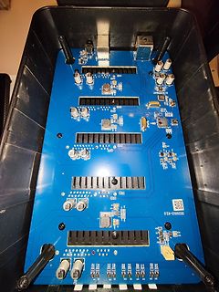
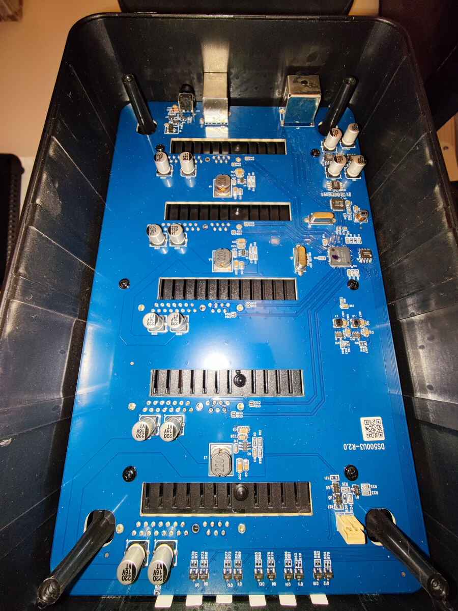
Blaue Leiterplatte in schwarzem Gehäuse
DS500U3-R2.0 220 16V 220 16V 220 16V 220 16V L1 L2 L3 L4 L5 L6 L7 L8 L9 L10 L11 L12 L13 L14 L15 L16 L17 L18 L19 L20 L21 L22 L23 L24 L25 L26 L27 L28 L29 L30 L31 L32 L33 L34 L35 L36 L37 L38 L39 L40 L41 L42 L43 L44 L45 L46 L47 L48 L49 L50 L51 L52 L53 L54 L55 L56 L57 L58 L59 L60 L61 L62 L63 L64 L65 L66 L67 L68 L69 L70 L71 L72 L73 L74 L75 L76 L77 L78 L79 L80 L81 L82 L83 L84 L85 L86 L87 L88 L89 L90 L91 L92 L93 L94 L95 L96 L97 L98 L99 L100 L101 L102 L103
in „Unbrick JMicron JMS567“ · Mikrocontroller und Digitale Elektronik · · Platinenfotos
-
PDF
30670055.pdf
Volumenteilen mit ver- schiedenen Materialkonstanten 47 1.7. Energieumwandlungen im elektromagnetischen Feld 53 1.7.1. Allgemeine Beziehungen 53 1:7.2. Der Poyntingsche Vektor 56 1.7.3. Energieströmung in stationären Feldern 58 1.7.4. Die Energiegleichung bei sinusförmigem zeitlichem Verlauf 62 1.7.5. Einige weitere
in „Wofür brauche ich Theoretische Elektrotechnik?“ · Ausbildung, Studium & Beruf ·
-
Bild
Leiterplatte eines Schaltnetzteils
CAUTION: FOR IMPROPER PROTECTION AGAINST RISK OF FIRE, REPLACE ONLY WITH SAME TYPE AND RATING OF FUSE. L1, L2, L3, L4, L5, L6, L7, L8, L9, L10, L11, L12, L13, L14, L15, L16, L17, L18, L19, L20, L21, L22, L23, L24, L25, L26, L27, L28, L29, L30, L31, L32, L33, L34, L35, L36, L37, L38, L39, L40, L41, L42, L43, L44, L45, L46, L47, L48, L49, L50, L51, L52, L53, L54, L55, L56, L57, L58, L59, L60, L61, L62, L63, L64, L65, L66, L67, L68, L69, L70, L71, L72, L73, L74, L75, L76, L77, L78, L79, L80, L81, L82, L83
in „Suche nach Bauteil“ · Analoge Elektronik und Schaltungstechnik · · Platinenfotos
-
PDF
buz30a.pdf
energy,periodic limitedjmaxT EAR 12 mJ Avalanche energy, single pulse EAS D = 21 A, DD = 50 V, GS = 25 L = 1.53 mH,jT = 25 ˚C 450 Gate source voltage V ± 20 V GS Power dissipation P W tot T = 25 ˚C 125 C Operating temperature T -55 ... + 150 ˚C j Storage temperature Tstg -55 ... + 150 Thermal resistance
in „Elektronische Last mit 2 MOSFETs“ · Analoge Elektronik und Schaltungstechnik ·
-
PDF
te2200.pdf
57 P41/AD1 P04/INTP4 20 56 P40/AD0 P05/INTP5 21 55 P87/A7 P06/INTP6 22 54 P86/A6 AVDD 23 53 P85/A5 AV REF0 24 52 P84/A4 P10/ANI0 25 51 P83/A3 26 2728 29 30 31 32 33 34 35 36 37 38 39 40 41 42 43 44 45 46 47 48 49 50 I 2I3 I 5I6 I I I S 0 1 E I 2 K I 1 K C UZ A 0 L A A A A A A A A A A A N N
in „LCD identifizieren.“ · Mikrocontroller und Digitale Elektronik ·
-
PDF
HBIS51V120.pdf
org 8100h 0011 8100 START: 0012 8100 12 0F52 lca l lIPLA 1 ;Scha l t e r s t e l lles e n 0013 8103 12 0F36 lca l lOPLA1 ;Zum Ausgab e p o r sch r e i b e n 0014 8106 30 B4 F7 jnb T0,START ;Wie d e r h o l bis T0=1 0015 8109 7F 00 mov r7,#0 0016 810B 12 20C5 lca l lOPLA1 ;Zu l e t z 00h ausge b e n 0017 810E 12 135F lca l lCLRAUTO ;Au t o s t a r t - Kennulös c h e n 0018 811 1 02 0000 l jmp 0 ;Neus t a r t 0019 8114 0020 8114 END 6.1.3 Bit abfragen Wird die INT0
in „8051 - Programm und Daten in einem 128kB Chip ohne Overlap“ · Mikrocontroller und Digitale Elektronik ·
-
PDF
Powersoft_DigiMod_1000_schematic.pdf
* 51 51 0 F F R t 1 V V V 1.0u5/16V A C 0 T 4 52 52 / 1 1 1 fl 5 ± 0 0 0 D 3 6 3 GND VDD 6 3 1 1 1 53 53 u C 0 0 C 2 . R ▯ / / / N 1 R50 54 54 9 0 N 0 0 N CN12 ▯ 0 u u u G 4 5 V 4 IN B OUT B 5 V 1.00K▯ ±1% 55 55 C . 5 5 ¡ 1 9 9 9 5 . V / H 1 0 R82 2 8 8 2 1 3 3 3 I HCPL-0611 1 5 TC4423EPA 1 1 A C m CN9
in „Powersoft DigiMod 1500 Endstufe - DC Offset am Ausgang“ · Analoge Elektronik und Schaltungstechnik ·
-
Bild
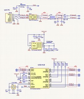
Schaltplan eines USB-Hubs mit CY7C65642-28LTXC
+5V_IN +3,3V_D L50 60 Ohm -3,3V_D -3,3V_A -3,3V_A GND-PAD C53 100nF C54 100nF C55 100nF CY7C65642-28LTXC VCC+3,3V USB-HUB R56 10K R57 10K R58 10K R59 10K D-Upload_N D-Kamera_N DM-1 DP+1 D-Kamera_P DM-1 DP-1 D-Upload_P
in „USB-Hub funktioniert nicht.“ · Mikrocontroller und Digitale Elektronik · · Schaltpläne
-
PDF
plan3.pdf
_P2 K5 3 R96 3 2 2 BC327-40 R79 BC327-40 1 1 T66 2 2 1 1 2 2 2 T54 2 R97T65 1 2K R80 K21 R98 2K 1 T53 FEDERKRAFTKLEMME605_T1_P2 IRF3205 3 1 2 1 1R81 2 1 3 IRF3205 2 271 127 2 2K 2K FEDERKRAFTKLEMME605_T1_P2 K6 3 BC327-40 R99 R82 3 BC327-40 2 T68 2 2 T56 1 1 R100 2 2 1 1 2 2 2 T67 1 2K 2K 1 T5583 K22
-
PDF
vergleichstabelle.pdf
.+165 °C >90 dB 0,12 dB 0,40 dB 0,73 dB 1,08 dB 2,08 dB Huber+Suhner Draht Ø 0,92 mm Ø 2,93 mm Ø 3,53 mm 4,14 mm 1179W 373W 215W 152W 87W l S 04272 B 18 GHz Cu vs PE-F AlF+CuG vz PE -40...+85 °C >90 dB 0,07 dB 0,24 dB 0,48 dB 0,75 dB 1,65 dB Low Loss b Huber+Suhner Draht Ø 1,4 mm Ø 3,83 mm Ø 4,48 mm
-
PDF
AMIS-30543-D.pdf
to EMC[1:0] = 01 140 V/ms MOTxx 10% EMC[1:0] = 10 70 V/ms EMC[1:0] = 11 35 V/ms DIGITAL OUTPUTS tH2L DO Output fall−time frominHto inL Capacitive load 400 pF and 50 ns ERR pullup resistor of 1.5 kW CHARGE PUMP CP CPN CPP Charge pump frequency 250 kHz tCPU MOTxx Startup time of charge pump Spec external
in „Puls aus Sinuswelle herausrechnen“ · Mikrocontroller und Digitale Elektronik ·
-
PDF
schema_stm32_primer2_1_2.PDF
220K 2 2 AUDIO_SDA 48 PB11/I2C_SDA PE2/TRACECLK/ FSMC_A23 1 CS_MEMS 2 1 1 AUDIO_I2S2_WS 51 2 JOYSTICK_L D11 D12 AUDIO_I2S2_SCK 52 PB12/SPI2_NSS PE3/TRACED0/FSMC_A19 3 JOYSTICK_R AUDIO_SPI_MISO 53 PB13/SPI2_SCK PE4/TRACED1/FSMC_A20 4 JOYSTICK_U AUDIO_I2S2_SD 54 PB14/SPI2_MISO PE5/TRACED2/FSMC_A21 5 JOYSTICK_D
in „STM32 USB Virtual COM Port“ · Mikrocontroller und Digitale Elektronik ·
-
Bild
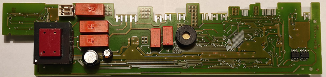
Foto einer bestückten Leiterplatte
L1, L2, L3, L4, L5, L6, L7, L8, L9, L10, L11, L12, L13, L14, L15, L16, L17, L18, L19, L20, L21, L22, L23, L24, L25, L26, L27, L28, L29, L30, L31, L32, L33, L34, L35, L36, L37, L38, L39, L40, L41, L42, L43, L44, L45, L46, L47, L48, L49, L50, L51, L52, L53, L54, L55, L56, L57, L58, L59, L60, L61, L62, L63, L64, L65, L66, L67, L68, L69, L70, L71, L72, L73, L74, L75, L76, L77, L78, L79, L80, L81, L82, L83
in „Bauteil gesucht - Transformator“ · Analoge Elektronik und Schaltungstechnik · · Platinenfotos
-
Bild
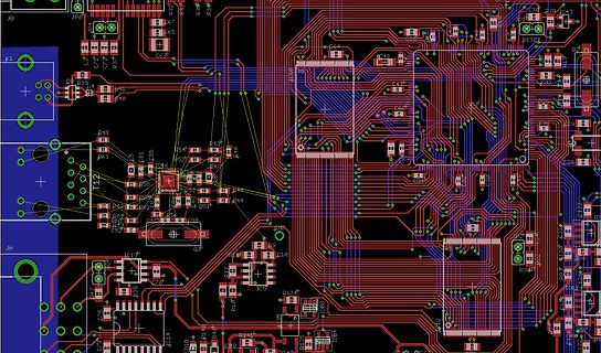
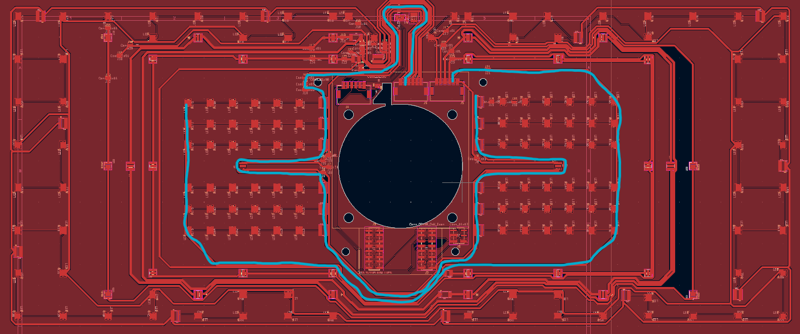
CAD-Ansicht eines Leiterplatten-Layouts
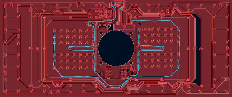
L1, L2, L3, L4, L5, L6, L7, L8, L9, L10, L11, L12, L13, L14, L15, L16, L17, L18, L19, L20, L21, L22, L23, L24, L25, L26, L27, L28, L29, L30, L31, L32, L33, L34, L35, L36, L37, L38, L39, L40, L41, L42, L43, L44, L45, L46, L47, L48, L49, L50, L51, L52, L53, L54, L55, L56, L57, L58, L59, L60, L61, L62, L63, L64, L65, L66, L67, L68, L69, L70, L71, L72, L73, L74, L75, L76, L77, L78, L79, L80, L81, L82, L83
in „LED-Platine summt“ · Analoge Elektronik und Schaltungstechnik · · Layouts
-
Bild
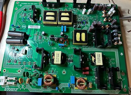
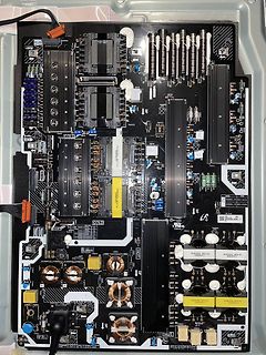
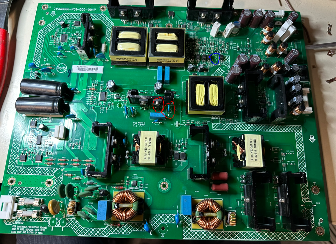
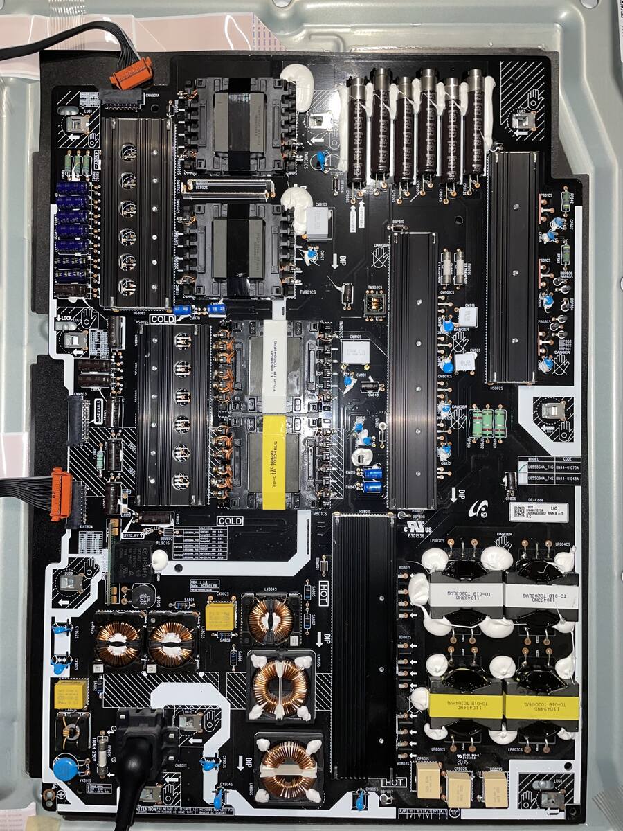
Leiterplatte eines Netzteils mit Kühlkörpern und Spulen
COLD HOT L1, L2, L3, L4, L5, L6, L7, L8, L9, L10, L11, L12, L13, L14, L15, L16, L17, L18, L19, L20, L21, L22, L23, L24, L25, L26, L27, L28, L29, L30, L31, L32, L33, L34, L35, L36, L37, L38, L39, L40, L41, L42, L43, L44, L45, L46, L47, L48, L49, L50, L51, L52, L53, L54, L55, L56, L57, L58, L59, L60, L61, L62, L63, L64, L65, L66, L67, L68, L69, L70, L71, L72, L73, L74, L75, L76, L77, L78, L79, L80, L81, L82, L83
in „Fernseher Defekt: Netzteil Schuld?“ · Analoge Elektronik und Schaltungstechnik · · Platinenfotos
-
PDF
441.pdf
Scheiben-Varistoren Aufbau SR: l Rechteckiger Varistorkörper in Vielschichttechnologie l Umhüllung: Epoxidharz, schwer entflammbar nach UL 94 V-0 l Anschlüsse: Kupferdraht, verzinnt S: l Runder Varistorkörper l Umhüllung: Epoxidharz
in „Fehlersuche bei Elektronischer Motorbremse: Phase vertauscht. Bauteile identifizieren“ · Analoge Elektronik und Schaltungstechnik ·
-
PDF
Command_Reference.pdf
Setting the change of direction............... 49 U ... Setting the error correction mode.......... 21 l (Pipe) ... Reading out the current record.....42 u ... Setting the minimum frequency............. 46 L ... Masking and demasking inputs..............29 l ... Setting the limit switch behaviour ......
in „SMCI-33 Schrittmotorsteuerung mit microcontroller“ · Mikrocontroller und Digitale Elektronik ·
-
PDF
DCF_77.pdf
Empfänger-IC 8; der,, Kleine” un terscheidet Versorgungsspannung Stromaufnahme (im Betrieb) :600 f l (< 1 mA) sich hiervon aber nur unwesentlich. (im Stand-by) :2@(<lOl_IA) Al A2 E3 AP2 CD CR Schaltstrom an PON (bei UPON= HIGH) : -15 f l ( < -50 @) APl Eingangsspannungsbereich Nachverstärker : 30...450 PV HF-Verstärkung an Al :53dB El Demodulator-Ausgangsspannung : 200 mVss Ausgangsstrom (Io,,) :max.lO@ Ausgangsstrom (Io, bei Ua I 200 mV) :min. 60 @ Ausgangsimpulsbreite (bei LOW-Bits) :100ms(c120ms) (bei HIGH-Bits) :200 ms (>
in „DCF77: Welcher Parallelkondensator?“ · HF, Funk und Felder ·
-
PDF
SSD1351-Revision_1.5.pdf
edge of E signal. Table 8-3 : Control pins of 6800 interface Function E R/W# CS# D/C# Write command ↓ L L L Read status ↓ H L L Write data ↓ L L H Read data ↓ H L H (1)e ↓ stands for falling edge of signal (2H stands for HIGH in signal (3L stands for LOW in signal In order to match the operating frequency
in „OLED128x128 SSD1351 RGB Initialisierung Color Farbe bunt SPI 3.3V AVR ATmega8 ATmega328p Assembler“ · Projekte & Code ·
-
Bild
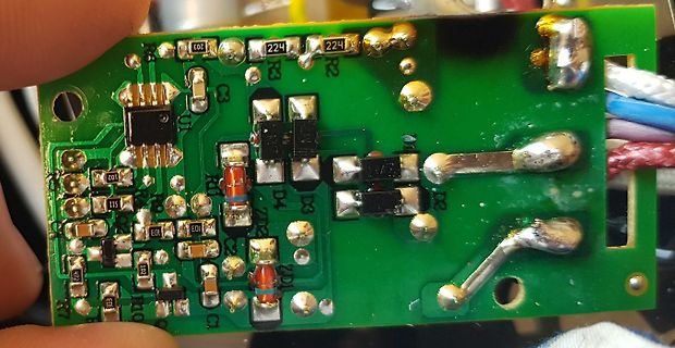
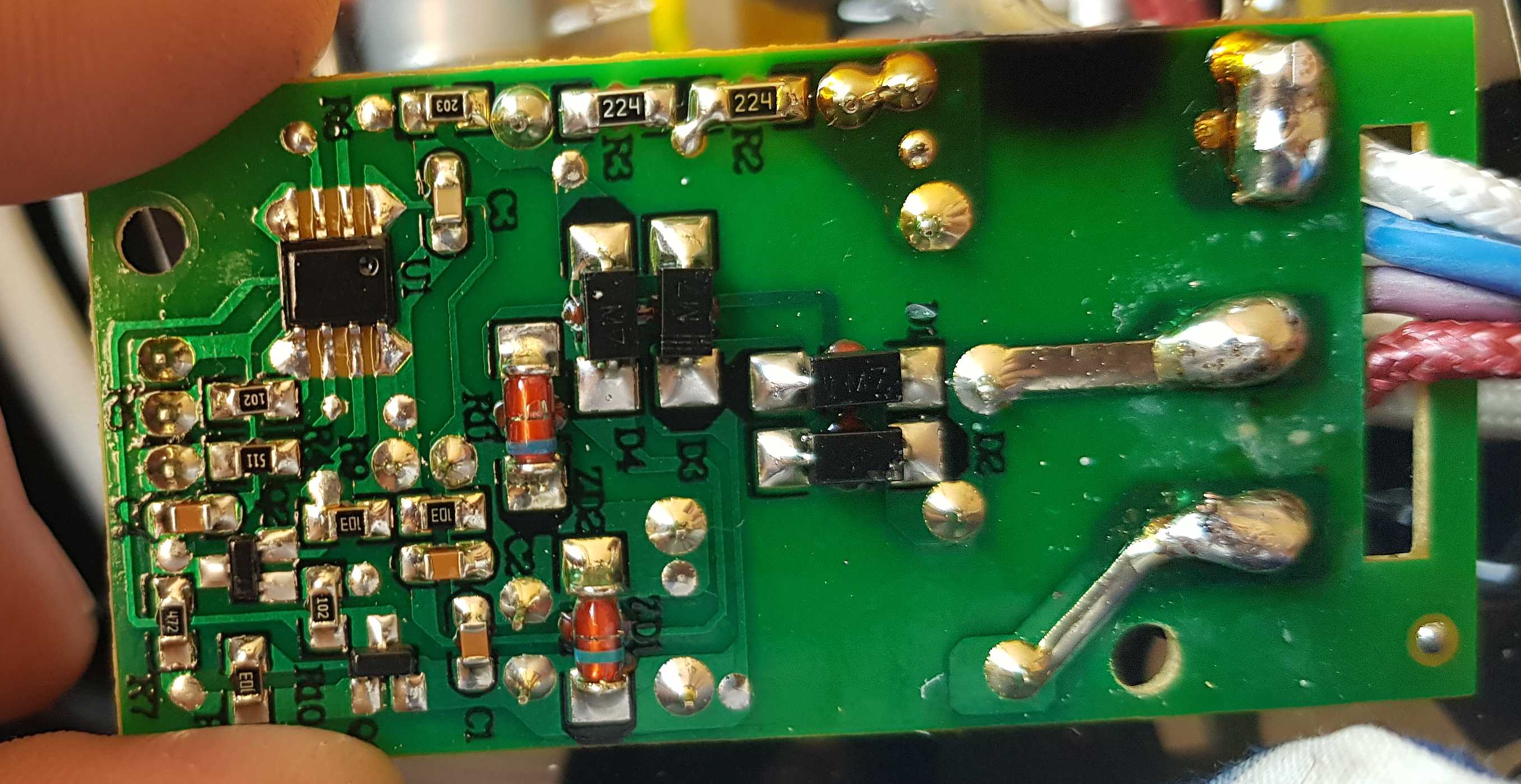
Foto einer bestückten Leiterplatte
C2, C3, R2, R3, D1, D3, D4, Q1, Q2, Q7, L1, L2, L3, L4, L5, L6, L7, L8, L9, L10, L11, L12, L13, L14, L15, L16, L17, L18, L19, L20, L21, L22, L23, L24, L25, L26, L27, L28, L29, L30, L31, L32, L33, L34, L35, L36, L37, L38, L39, L40, L41, L42, L43, L44, L45, L46, L47, L48, L49, L50, L51, L52, L53, L54, L55, L56, L57, L58, L59, L60, L61, L62, L63, L64, L65, L66, L67, L68, L69, L70, L71, L72, L73, L74, L75, L76, L77, L78, L79, L80, L81, L82, L83
in „Wert des Widerstandes“ · Analoge Elektronik und Schaltungstechnik · · Platinenfotos
-
Datei
Synth.asm
0 ldi rkeyoff, 0 loop: ; 1. Phasenakkumulation ;aus SRAM laden ldd rpkl, Y+1 ldd rpkh, Y+2 ldd rp1l, Y+3 ldd rp1h, Y+4 add rp1l, rpkl adc rp1h, rpkh std Y+3, rp1l std Y+4, rp1h ;Low interessiert mich nich mehr ;rp1h hat jetzt 256 bits Aufloesung, mov rmp, rp1h ;Position der Daten auf der LUT ldi ZH
in „Attiny2313 Timer16 Bit, Normal Mode, unsauber“ · Mikrocontroller und Digitale Elektronik ·
-
PDF
DOC1473.pdf
detected brge fault ;within 130ms then exit sbic PIND,INPUT ;Wait for start bit rjmp start1 clr timerL ;Measure length of start bit start2: cpi timerL,17 ;If startbit longer than 1.1ms, brge fault ;exit sbis PIND,INPUT rjmp start2 ;Positive edge of 1st start bit mov temp,timerL ;timer is 1/2 bit time clr timerL mov ref1,temp lsr ref1 mov ref2,ref1 add ref1,temp ;ref1 = 3/4 bit time lsl temp add ref2,temp ;ref2 = 5/4 bit time start3: cp timerL,ref1 ;If high period St2 > 3/4 bit time brge fault ;exit sbic PIND
in „IR-Empfänger“ · Mikrocontroller und Digitale Elektronik ·
-
PDF
AVR410_RC5_IR_Remote_Control_Reciver.PDF
detected brge fault ;within 130ms then exit sbic PIND,INPUT ;Wait for start bit rjmp start1 clr timerL ;Measure length of start bit start2: cpi timerL,17 ;If startbit longer than 1.1ms, brge fault ;exit sbis PIND,INPUT rjmp start2 ;Positive edge of 1st start bit mov temp,timerL ;timer is 1/2 bit time clr timerL mov ref1,temp lsr ref1 mov ref2,ref1 add ref1,temp ;ref1 = 3/4 bit time lsl temp add ref2,temp ;ref2 = 5/4 bit time start3: cp timerL,ref1 ;If high period St2 > 3/4 bit time brge fault ;exit sbic PIND
in „Universeller RC5-Fernbedienungsempfänger“ · Mikrocontroller und Digitale Elektronik ·
-
Datei
spicemodel.txt
ORDER 1=Vcc 2=IN 3=Vee 4=SINK 5=NC 6=SOURCE .SUBCKT ZXGD3009DY 1 2 3 4 5 6 Q1 10 2 60 N Q2 30 2 40 P L1 1 10 1p L2 3 30 1p L3 4 40 100p L4 6 60 100p .MODEL N NPN(IS=6E-14 BF=500 NF=.98 ISE=1E-14 NE=1.25 ISC=3.3E-14 BR=15 NR=1 NC=1.12 CJE=36.592p VJE=.75 MJE=.37 CJC=9.674p VJC=.5 MJC=.33 VAF=28 IKF=1 RC
in „LTSpice - hierarchische Blöcke“ · Analoge Elektronik und Schaltungstechnik ·
-
Datei
NTC.html
org/2000/svg' viewBox='0 0 16 16'%3e%3cpath fill-rule='evenodd' clip-rule='evenodd' d='M12 5c-.28 0-.53.11-.71.29L7 9.59l-2.29-2.3a1.003 1.003 0 00-1.42 1.42l3 3c.18.18.43.29.71.29s.53-.11.71-.29l5-5A1.003 1.003 0 0012 5z' fill='white'/%3e%3c/svg%3e"); } .bp3-control.bp3-checkbox input:indeterminate ~
in „NTC auto kalibrierung - Matheformel“ · Mikrocontroller und Digitale Elektronik ·
-
PDF
ln_423_425_3005XIII_schaltplan.pdf
150 1M 220k INT E2 AB2 47 104 7 C20 34 22 AD3 AC2 46 +5V +5V +5V OP07C -V V- D3 AD2 45 104 R68 224 L 4 R50 +8V 4.7K N G C A G B P A E F B AE2 44 3.0k C18 R17 AG2 43 104 C34 AF2 42 471 3 2 1 0 9 8 7 6 5 4 3 AA2 41 R9 10k 3 2 3 3 3 P 2 24 3 3 3 ADP2 40 VREF VB VB G C A G B A E F B AB3 39 10k A A A A A
in „Labornetzgerät LN-423/425, 3005XIII, McPower 2x30V/5A - Verbesserungen u. Änderungen“ · Analoge Elektronik und Schaltungstechnik ·
-
PDF
SBR10U40CTFP.pdf
° ITO-220AB B ° 5 Dim Min Typ Max Q A 4.50 4.70 4.90 B A1 3.04 3.24 3.44 D 5° A2 2.56 2.76 2.96 D1 L1 b 0.50 0.60 0.75 5 5° b1 1.10 1.20 1.35 c 0.50 0.60 0.70 D 15.67 15.87 16.07 b1 3x A2 D1 8.99 9.19 9.39 e 2.54 E 9.91 10.11 10.31 L b 3x L 9.45 9.75 10.05 e e L1 15.80 16.00 16.20 P 2.98 3.18 3.38 3
in „Aufwärtsschaltregler bauen“ · Analoge Elektronik und Schaltungstechnik ·
-
PDF
MSV30245_Schematic_RevB.pdf
49 47 48 50 P9_2 P9_2 100 P12/D10 75 D11 WRH 51 49 50 52 P8_4 C18 P9_3 99 P92/SOF P13/D11 74 D12 RD 53 51 52 54 P8_3 R20 0.47uF P93/ADTrg P14/D12 73 D13 VCC BCLK 55 53 54 56 P8_2 P15/D13 72 D14 VCC HLDA 57 55 56 58 P8_1 2 1.5K P16/D14 57 58 3 UVcc P17/D15 71 D15 HOLD 59 59 60 60 P8_0 ALE 61 61 62 62 P7
in „m16C on Chip Programmierung“ · Mikrocontroller und Digitale Elektronik ·
-
PDF
BC1604A_series_VER01.pdf
Vdd 5.0V Supply Voltage for logic (option +3.0V) 3 Vo (Variable) Operating voltage for LCD 4 RS H/L H: DATA, L: Instruction code 5 R/W H/L H: Read(MPU¡÷ Module) L: Write(MPU¡÷ Module) 6 E H,H¡÷ L Chip enable signal 7 DB0 H/L Data bit 0 8 DB1 H/L Data bit 1 9 DB2 H/L Data bit 2 10 DB3 H/L Data bit 3
-
PDF
Baumappe_BX-222P_1_.pdf
C47 100n VREF V M P 4 VRN IC3 5 VRP O UDA1361TS 100n 15 VSSA N N T K S 16 VDDA V V D B W 1 3 3 2 C53 + C52 1 1 1 33u 100n R40 2k2 W S/1.1B BCK/1.1B R39 2k2 DATAO/1.1B GNDA B B . 5 . / 2 / L R Bild A1: I N Schaltplan der Onboard-Soundkarte V V R16 R17 X1 TP2 I I L1 MINI-USB TXD 100k W W 10k VCC _ _ A
-
Bild
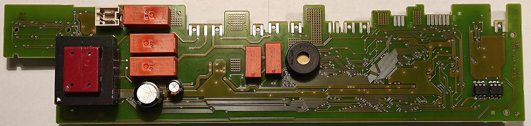
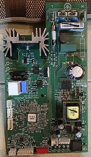
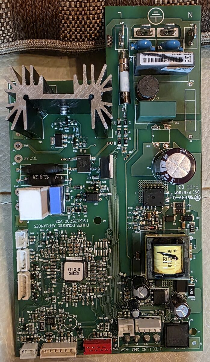
Bestückte Leiterplatte eines Philips Haushaltsgeräts
L N L1 L2 L3 L4 L5 L6 L7 L8 L9 L10 L11 L12 L13 L14 L15 L16 L17 L18 L19 L20 L21 L22 L23 L24 L25 L26 L27 L28 L29 L30 L31 L32 L33 L34 L35 L36 L37 L38 L39 L40 L41 L42 L43 L44 L45 L46 L47 L48 L49 L50 L51 L52 L53 L54 L55 L56 L57 L58 L59 L60 L61 L62 L63 L64 L65 L66 L67 L68 L69 L70 L71 L72 L73 L74 L75 L76 L77 L78 L79 L80 L81 L82 L83 L84 L85 L86 L87 L88 L89 L90 L91 L92 L93 L94 L95 L96 L97 L98 L99 L100 L101 L102
in „Steuerkarte Philips Kaffeautomat“ · Analoge Elektronik und Schaltungstechnik · · Platinenfotos
-
Datei
PWM-Sinus.asm
MOVWF PR2 ; 2,5 kHz BCF STATUS,RP0 ; Bank1 ; Tastverhältnis auf 50% einstellen MOVLW D'0' MOVWF CCPR1L ; 50% von 124 MOVWF CCPR2L ; RC2/CCP1 auf Ausgang stellen BSF STATUS,RP0 ; Bank1 BCF TRISC, 2 ; RC2: output=0 BCF STATUS,RP0 ; Bank 0 ; PWM MODE mit CCP1 initialisieren CLRF CCP1CON ; CCP1-Modus aus
in „Theorie Wechselrichter 12V DC -> 230V AC“ · Analoge Elektronik und Schaltungstechnik ·
-
PDF
SCM1.pdf
TT240 gk 3.95*** RMS-30 200-3000 DC-1000 6.5 .20 9.0 9.8 27 (typ.) 17 (min.) 20 (typ.) 7 (min.) 1-53 TT240 w 6.95*** RMS-860 800-1050 DC-250 5.5 .23 7.5 7.5 36 (typ.) 25 (min.) 24 (typ.) 18 (min.) 1-171 TT100 w 11.45 L=lowrange[f to10f] M=midrange[10f tof /2] U=upperrange[f /2tof ] L L L U U U m=midband
in „[V] SL11H, USS720E ua.“ · Markt ·
-
Bild
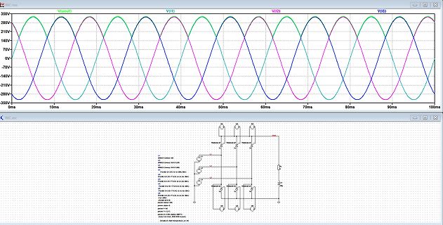
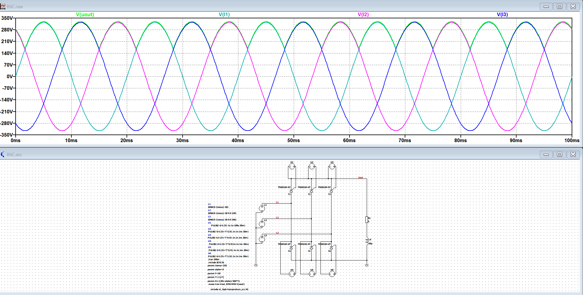
LTspice Simulation Schaltplan und Wellenformen
0V -70V -140V -210V -280V -350V 0ms 10ms 20ms 30ms 40ms 50ms 60ms 70ms 80ms 90ms 100ms tscraw.asc L1 L2 L3 L4 L5 L6 L7 L8 L9 L10 L11 L12 L13 L14 L15 L16 L17 L18 L19 L20 L21 L22 L23 L24 L25 L26 L27 L28 L29 L30 L31 L32 L33 L34 L35 L36 L37 L38 L39 L40 L41 L42 L43 L44 L45 L46 L47 L48 L49 L50 L51 L52 L53 L54 L55 L56 L57 L58 L59 L60 L61 L62 L63 L64 L65 L66 L67 L68 L69 L70 L71 L72 L73 L74 L75 L76 L77 L78 L79 L80 L81 L82 L83 L84 L85 L86 L87 L88 L89 L90 L91 L92 L93 L94 L95 L96 L97 L98 L99 L100 L101 L102 L103
in „LTSpice Simulation B6C gesteuert“ · Analoge Elektronik und Schaltungstechnik · · Screenshots
-
PDF
SSD1332.pdf
( . COM62 RES# r . COM60 CS# i . D/C# D E (RD#) r n . R/W#(WR#) d o . | BS2 c m . D o . COM2 BS1 A l C . COM0 BS0 e R c . U f D S C e G r . D7 M I G D6 D5 SA0 D4 . SB0 D3 . SC0 D2 SA1 D1 . D0 e . SB1 r . SC1 D . n . | m . e S . V DD . SA95 VSS . SB95 SC95 . . r r g E k . n r t a n a l e L l ) a d l
in „Verkaufe OLED Displays FullColor 128*128 bzw. 96*64“ · Markt ·
-
Bild
CAD-Ansicht eines Leiterplatten-Layouts
JB, JB4, R35, R34, C10, R20, C24, JB6, C65, C67, C28, RESET, L5, C63, C64, C48, C51, C53, C33, C35, C31, C29, R33, R41, R40, R48, R54, R42, R63, IC6, R52, R51, R45, R44, R53, R43, R46, R47, C92, C93, IC4, Q3, R9, R10, C10, IC5, R12, R13, R14, R11, R15, R16, R17,
in „Umstieg auf 6 Lagen? Welche Signale wohin?“ · Platinen · · Layouts
-
PDF
ADS8364.pdf
vs TEMPERATURE vs TEMPERATURE 3 4 ) ) B S 3 L 2 ( ( L N I 2 D 1 m m m 1 m x x 0 a a d 0 d n n–1 a a u –1 u i i–2 i –2 i M M –3 –3 –50 –25 0 25 50 75 100 –50 –25 0 25 50 75 100 Temperature (°C) Temperature (°C) FREQUENCY SPECTRUM INTEGRAL LINEARITY
in „ADC ADS8364 ansprechen“ · Mikrocontroller und Digitale Elektronik ·
-
PDF
MSM5299AGS-K.pdf
O71 21 60 O10 O72 22 59 O9 O73 23 58 O8 O74 24 57 O 7 O75 25 56 O6 O76 26 55 O5 O 27 54 77 O4 O78 28 53 O3 O79 29 52 O2 O 30 51 80 O1 3 3 3 3 3 3 3 3 3 4 4 4 4 4 4 4 4 4 4 5 E 4 3 1 F D S E N VE V V V N D O D H S D D D D CP C N AD E P V S V O D L NC : No connection 100-Pin Plastic QFP Note: The abbreviated
in „ansteuerung von grafikdisplay UG-32F01“ · Mikrocontroller und Digitale Elektronik ·
-
PDF
msm5299a.pdf
O71 21 60 O10 O72 22 59 O9 O73 23 58 O8 O74 24 57 O 7 O75 25 56 O6 O76 26 55 O5 O 27 54 77 O4 O78 28 53 O3 O79 29 52 O2 O 30 51 80 O1 3 3 3 3 3 3 3 3 3 4 4 4 4 4 4 4 4 4 4 5 E 4 3 1 F D S E N VE V V V N D O D H S D D D D CP C N AD E P V S V O D L NC : No connection 100-Pin Plastic QFP Note: The abbreviated
in „Optrex DMF50191N“ · Mikrocontroller und Digitale Elektronik ·