-
PDF
irfp2907.pdf
PD -93906B IRFP2907 AUTOMOTIVE MOSFET ® HEXFET Power MOSFET Typical Applications l Integrated Starter Alternator D V DSS = 75V l 42 Volts Automotive Electrical Systems Benefits R = 4.5mΩ l Advanced Process Technology G DS(on) l Ultra Low
in „Sinusendstufe für 300A“ · Mikrocontroller und Digitale Elektronik ·
-
PDF
IRFP2907.pdf
PD -93906B IRFP2907 AUTOMOTIVE MOSFET ® HEXFET Power MOSFET Typical Applications l Integrated Starter Alternator D V DSS = 75V l 42 Volts Automotive Electrical Systems Benefits R = 4.5mΩ l Advanced Process Technology G DS(on) l Ultra Low
in „Auto-Kühler-Lüfter per PWM manuell steuern“ · Analoge Elektronik und Schaltungstechnik ·
-
PDF
Anhang3.pdf
的其他特点包括电池温度检测、欠压闭锁、自动再充电和两个 用于指示充电、结束的 LED 状态引脚。 特点 绝对最大额定值 ·高达 1000mA 的可编程充电电流 ·输入电源电压(V ) :-0.3V~8V CC ·无需 MOSFET、检测电阻器或隔离二极管 ·PROG:-0.3VCC +0.3V ·用于单节锂离子电池、采用 ESOP 封装的完整 ·BAT:-0.3V~7V 线性充电器 · :-0.3V~10V ·恒定电流/恒定电压操作,并具有可在无过热 · :-0.3V~10V 危险的情况下实现充电速率最大化的热调节 ·TEMP:-0.3V~10V 功能 ·CE:-0.3V~10V ·BAT 短路持续时间:连续 ·精度达到
in „sichere Umsetzung Schutzabschaltung Akku“ · Analoge Elektronik und Schaltungstechnik ·
-
PDF
RequiresAcrobat6.pdf
has been downloaded from http://www.datasheetarchive.com. GF9926 Dual N-Channel Enhancement-Mode MOSFET LowV GS(th) V DS 20V R DS(ON) 30 ΩmI 6.0AD H C ® E N T R E T F D1 D1 D2 D2 E N 8 7 6 5 G SO-8 0.189 (4.80) Q1 Q2 8 5 1 2 3 4 0.157 (3.99) 0.150 (3.81) S1 G1 S2 G2 0.244 (6.20) 0.228 (5.79) 1 4 Dimensions
in „Ersatz-MosFet für GF9926“ · Analoge Elektronik und Schaltungstechnik ·
-
PDF
BTS7960_v1.1_2004-12-07.pdf
applications. It is part of the P-TO-263-7 TM NovalithIC family containing one p-channel highside MOSFET and one n-channel lowside MOSFET with an integrated driver IC in one package. Due to the p-channel highside switch the need for a charge pump is eliminated thus minimizing EMI. Interfacing to a microcontroller
in „H-Brücke für Gleichstrommotor 24V 5A“ · Analoge Elektronik und Schaltungstechnik ·
-
PDF
Infineon-BTS7960-DS-v01_01-en.pdf
applications. It is part of the P-TO-263-7 TM NovalithIC family containing one p-channel highside MOSFET and one n-channel lowside MOSFET with an integrated driver IC in one package. Due to the p-channel highside switch the need for a charge pump is eliminated thus minimizing EMI. Interfacing to a microcontroller
in „BTS7960 IS Sensor mit abweichenden Werten.“ · Analoge Elektronik und Schaltungstechnik ·
-
PDF
BTS7960_v1.1_2004-12-07.pdf
applications. It is part of the P-TO-263-7 TM NovalithIC family containing one p-channel highside MOSFET and one n-channel lowside MOSFET with an integrated driver IC in one package. Due to the p-channel highside switch the need for a charge pump is eliminated thus minimizing EMI. Interfacing to a microcontroller
in „H-Brücken IC schalten bei Belastung ab und nicht wieder an“ · Mikrocontroller und Digitale Elektronik ·
-
PDF
Schaltungskonzepte_zum_Betrieb_von_Leuchtdioden_fuer_die_Allgemeinbeleuchtung.pdf
abgeschätzt wurden, beinhaltet der gemessene Wert auch die Verluste in den KomponentenfürRegelungundMOSFET-Ansteuerung. EinAustausch des MOSFETs mit dem SPD02N60C3 bestätigt Bild 3.8. Es ist keine signifikante Abwei- chung im Wirkungsgrad messbar. 40 3 Einstufige Konverter mit Regelung des Ausgangsstroms
in „PFC? Wozu diese Ladekondensatorschaltung im Schaltnetzteil?“ · Analoge Elektronik und Schaltungstechnik ·
-
PDF
Sinuswechselrichter.pdf
sichwird erst aufladen muss, steigt die Spannung am Gate des MOSFET kontinuierlich. Derich MOSFET durchläuft für einige Zeit den Sättigungsbereich, der durch eine erhöhten MOSFET durchläuft DSr ein ge Zeit den Sättigungsbereich, der durch einen rhöhteniese Spannungsabfall
in „Wechselrichter Spannung und Frequenz steuerbar für Teichpumpe“ · Haus & Smart Home ·
-
PDF
isl78225.pdf
polarity of the PWM output signal. Pulling this pin to GND will force normal operation with inverting MOSFET drivers. Pulling this pin to VCC will invert the PWM signal for operation with non-inverting MOSFET drivers. This function provides the flexibility for the ISL78225 to work with different drivers.
in „Verdammtes Kompensationsnetzwerk“ · Analoge Elektronik und Schaltungstechnik ·
-
PDF
tps5431.pdf
THERMAL SHUTDOWN Thermal shutdown trip point 135 162 °C Thermal shutdown hysteresis 14 °C OUTPUT MOSFET VIN = 5.5 V 150 DS(on) High-side power MOSFET switch 110 230 m 3 Submit Documentation Feedback TPS5430 TPS5431 www.ti.com SLVS632C–JANUARY 2006–REVISED NOVEMBER 2006 PIN ASSIGNMENTS DDA PACKAGE (TOP
in „Warum neigt ein (Stepdown) Regler mit Keramik Cs zum schwingen?“ · Analoge Elektronik und Schaltungstechnik ·
-
PDF
LTC4067.pdf
ExternalIdealDiodeGateConnection.This H L 2 CLDIS pin controls the gate of an optional external P-channel MOSFET transistor used to supplement the internal ideal ThemaximumCLPROGresistancevalueshouldbenomore diode. The source of the P-channel MOSFET should be than 5k. Ground to disable the current limit function
in „LTC4067 Vout“ · Analoge Elektronik und Schaltungstechnik ·
-
PDF
mp2307.pdf
buck • 3A Continuous Output Current regulator. The device integrates 100mΩ 4A Peak Output Current MOSFETS that provide 3A of continuous load • Wide 4.75V to 23V Operating Input Range current over a wide operating input voltage of • Integrated 100mΩ Power MOSFET Switches 4.75V to 23V. Current mode control
in „Spannungsregelung mit MP1584 und MP2307“ · Mikrocontroller und Digitale Elektronik ·
-
PDF
mp2307.pdf
buck • 3A Continuous Output Current regulator. The device integrates 100mΩ 4A Peak Output Current MOSFETS that provide 3A of continuous load • Wide 4.75V to 23V Operating Input Range current over a wide operating input voltage of • Integrated 100mΩ Power MOSFET Switches 4.75V to 23V. Current mode control
in „Step Down - Stabil 5V 3A“ · Analoge Elektronik und Schaltungstechnik ·
-
PDF
mp2307.pdf
buck • 3A Continuous Output Current regulator. The device integrates 100mΩ 4A Peak Output Current MOSFETS that provide 3A of continuous load • Wide 4.75V to 23V Operating Input Range current over a wide operating input voltage of • Integrated 100mΩ Power MOSFET Switches 4.75V to 23V. Current mode control
in „Empfehlung Step Down Converter IC“ · Analoge Elektronik und Schaltungstechnik ·
-
PDF
2207251030_Mixic-MX1616H_C5119044-1.pdf
and P-channel power MOSFETs. — 1 channel 1.6A power tube internal resistance 0.4 ohm The voltage range covers 2V to 8.6V. 27ÿ, VDD=6.5V, two — 2 channels 1.6A power tube internal resistance 0.4 ohm Under the condition that the
in „MX1616H Dual H-Bridge Motor Driver“ · Analoge Elektronik und Schaltungstechnik ·
-
PDF
Viper12a.pdf
at which the device stops switching and turns on DDoff the start up current source. SOURCE Power MOSFET source and circuit ground reference. Power MOSFET drain. Also used by the internal high voltage current source during DRAIN start up phase for charging the externDD capacitor. Feedback input. The useful
in „Reparatur Netzteil elektrischer Kamin“ · Analoge Elektronik und Schaltungstechnik ·
-
PDF
GWM120-0075P3.pdf
GWM 120-0075P3 Three phase full bridge V DSS = 75 V with Trench MOSFETs ID25 = 125 A in DCB isolated high current package R DSon typ. = 3.7 m Ω L+ P is Gate G3 G1 G5 S3 S5 S1 L1 L2 L3 G4 G6 G2 ns S4 S6 P owerP i S2 L - Applications MOSFETs AC drives Symbol Conditions
in „Umrichter für E-Kart Anwendung 60V / 120A“ · Mikrocontroller und Digitale Elektronik ·
-
PDF
9x.23_light-power.pdf
lateddcsourceforhigh-sidegatedrive.We sawthisbackin §3.5.6B,whereaPVI5033(dual-channelLEDtoPV-stack) was used to generate MOSFET gate drive (Fig. 3.107A). Parts like that can create enoughbias to switch a MOSFET, but they are feeble, and slow: the PVI5033’s photovoltaic stack generates 5–10V, with a short-circuit current of
in „Differenztastkopf 200Mhz“ · Analoge Elektronik und Schaltungstechnik ·
-
PDF
OB2223CPA.pdf
frequency voltage. simplification.nts are required for PCB design The internal power MOSFET in OB2223 is driven At light load or zero load condition, most of the iy a dedicated gate driver for power switch control. supply is from switching loss on the MOSFET. n f conduction and switch loss of MOSFET while toogher the maswitchingf frequency. isLowerropswioching A good tradeoff is achieved through the built-in frequency leads to the reduction on the power totem pole gate design with right output
in „SMD IC "G1768A" Datenblatt gesucht“ · Analoge Elektronik und Schaltungstechnik ·
-
PDF
VNS1NV04DTR.pdf
® VNS1NV04D “OMNIFET II”: FULLY AUTOPROTECTED POWER MOSFET TYPE RDS(on) Ilim Vclamp VNS1NV04D 250 m (*) 1.7 A (*) 40 V (*) (*) Per each device n LINEAR CURRENT LIMITATION n THERMAL SHUT DOWN n SHORT CIRCUIT PROTECTION n INTEGRATED CLAMP n LOW CURRENT DRAWN
in „[V] Highside-Schalter“ · Markt ·
-
PDF
Vollbr_cke_VNH3SP30.pdf
that allows to efficiently LOSS OF GROUND AND LOSS OF V CC integrate on the same die a true Power MOSFET with an intelligent signal/protection circuitry. The Low-Side switches are vertical MOSFETs manufactured using STMicroelectronics proprietary EHD (“STripFET™”) process. BLOCK DIAGRAM V CC O + U OVERTEMPERATURE
in „VNH3SP30 auch als Halbbrücke“ · Mikrocontroller und Digitale Elektronik ·
-
PDF
infineon-ug-202311-pl52-2312-121012-solid-state-circuit-breaker-reference-design-user-guide-usermanual-en.pdf
Thisuserguidedescribesthesetupandevaluationofthe solid-statecircuitbreaker(SSCB) referencedesigns basedonCoolMOS™S7TandCoolSiC™powerMOSFETs:REF_SSCB_AC_DC_1PH_16A and REF_SSCB_AC_DC_1PH_SiC.Itprovidesabrief overviewof theSSCBreference designconcept, functions,and protectionanddiagnosisimplementations. Intendedaudience Thisdocumentis intendedforengineers
in „Leitungsschutzschalter 24VAC“ · Analoge Elektronik und Schaltungstechnik ·
-
 Bild
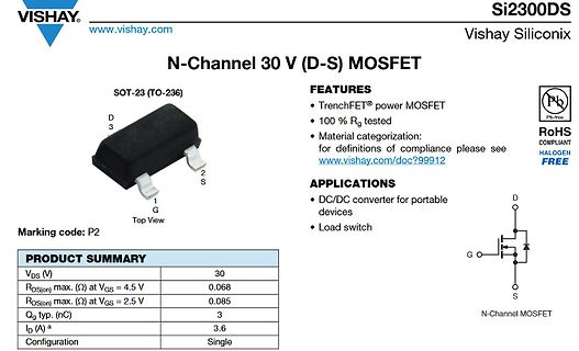
Datenblatt eines N-Channel 30 V MOSFETs
VISHAY Si2300DS www.vishay.com N-Channel 30 V (D-S) MOSFET FEATURES TrenchFET power MOSFET 100 % Rg tested Material categorization: for definitions of compliance please see www.vishay.com/doc?99912 APPLICATIONS DC/DC converter for portable devices Load switch
in „ESP32 hängt wenn Spannung von 0V ansteigt -> reset bis 14 V Solarspannung“ · Mikrocontroller und Digitale Elektronik · · Screenshots
-
PDF
Kommunikationsprotokoll_der_VB-Serie-DE.pdf
Series •2 Byte: Die vierte Batteriezellenspannung, wobei das niedrige Byte das ersteist. • 2Byte: MOSFET-Temperatur, zuerst Low-Byte. • 2Byte: Zelltemperatur, zuerst niedriges Byte. • 4Byte: SOC, Batterieprozentsatz, Low-Byte zuerst. • 4 Byte: Gesamtbatteriespannung, Low Byte zuerst. • 4Byte: Strom (in
in „Amateure braucht Hilfe bei RS232“ · Mikrocontroller und Digitale Elektronik ·
-
PDF
lm5642.pdf
to the low side of the current sense resistor that is placed between VIN and the drain of the top MOSFET. When the Rds of the top MOSFET is used for current sensing, connect this pin to the source of the top MOSFET. Always use a separate trace to form a Kelvin connection to this pin. SW2 (Pin 16) Switch-node
in „Komisches Verhalten von LM5642MTCX“ · Analoge Elektronik und Schaltungstechnik ·
-
PDF
Intersil_HIP4081A_.pdf
power MOSFET. 14 ALS A Low-side Source connection. Connect to source of A Low-side power MOSFET. 15 V Positive supply to gate drivers. Must be same potenti(Pin 16). Connect to anodes of two bootstrap diodes. CC
in „Umrichter für E-Kart Anwendung 60V / 120A“ · Mikrocontroller und Digitale Elektronik ·
-
PDF
MAX16801A-MAX16802B.pdf
amplifier is soft-started. This method results in superio/ control of the LED current. B n-Channel MOSFET Switch Driver / 100ms/div The NDRV pin drives an external n-channel MOSFET. M The NDRV output is supplied by the internal regulator A (VCC ), which is internally set to approximately +9.5V. Figure
in „High Brightness LEDs > 50W µC als regelbare KSQ“ · Mikrocontroller und Digitale Elektronik ·
-
PDF
lm3444.pdf
Circuit ground connection. 7 4 ISNS LED current sense pin. Connect a resistor from main switching MOSFET source, ISNS to GND to set the maximum LED current. 8 5 GATE Power MOSFET driver pin. This output provides the gate drive for the power switching MOSFET of the buck controller. 9 6 V Input voltage
in „High Brightness LEDs > 50W µC als regelbare KSQ“ · Mikrocontroller und Digitale Elektronik ·
-
PDF
Mitsubishi_2m_Modul_RA60H1317M1.pdf
136-174MHz 60W 12.5V, 2 Stage Amp. For MOBILE RADIO DESCRIPTION The RA60H1317M1A is a 60-watt RF MOSFET Amplifier BLOCK DIAGRAM Module for 12.5-volt mobile radios that operate in the 136- to 174-MHz range. 2 3 The battery can be connected directly to the drain of the enhancement-mode MOSFET transistors
in „Linearisierung von HF-Endstufen“ · HF, Funk und Felder ·
-
 Bild
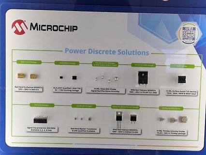
Microchip Werbeübersicht für Power Discrete Solutions
Packages (D-Melf, B-Melf, A-Melf, C-Melf) TO-247 CLC SMD Package PLAD Package Rad-Hard N-channel MOSFETs 100V - 250V in SMD-0.5 DLA JANP Qualified 1.5kW TVS 5V - 175V Working Voltage HI-REL Glass SMD Diodes Signal/Rectifier/Zener/Schottky MNS Rad-Tolerant MOSFETs 100V - 250V in TO-247 CLC SMD HI-REL
in „SpaceTechExpo, Tag 2 – Bauteile, Bauteile, Bauteile“ · Mikrocontroller und Digitale Elektronik · · Fotos
-
 Bild
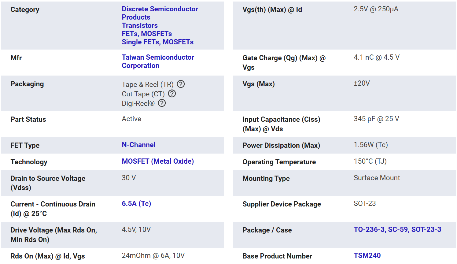
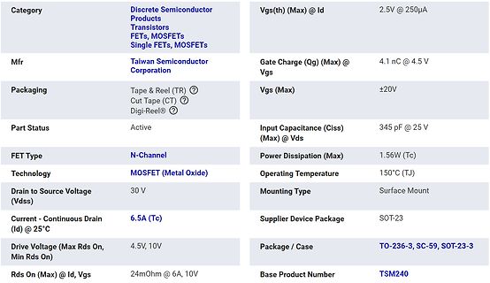
Technische Daten eines N-Kanal MOSFETs
Category Discrete Semiconductor Products Transistors FETs, MOSFETs Single FETs, MOSFETs Mfr Taiwan Semiconductor Corporation Packaging Tape & Reel (TR) Cut Tape (CT) Digi-Reel® Part Status Active FET Type N-Channel Technology MOSFET (Metal Oxide) Drain to Source
in „Ersatz für MOSFET nexperia PMV20ENR“ · Analoge Elektronik und Schaltungstechnik · · Screenshots
-
 Bild
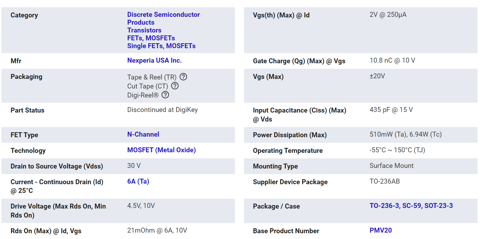
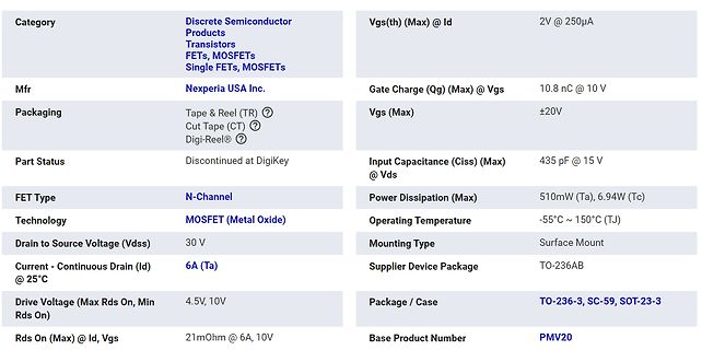
Technische Daten eines N-Kanal MOSFETs
Category Discrete Semiconductor Products Transistors FETs, MOSFETs Single FETs, MOSFETs Mfr Nexperia USA Inc. Packaging Tape & Reel (TR) Cut Tape (CT) Digi-Reel (R) Part Status Discontinued at DigiKey FET Type N-Channel Technology MOSFET (Metal Oxide) Drain to Source
in „Ersatz für MOSFET nexperia PMV20ENR“ · Analoge Elektronik und Schaltungstechnik · · Screenshots
-
PDF
Schaltplan_DMS_Messverstaerker.pdf
R42 5V_USB VCCIO 0Ω 10kΩ 100nF 2.2kΩ 1 3.3kΩ 1Ω Q20 NTC TPS73601 IN OUT H H Q14 EN NNR/FB R31 C41 MOSFET-N_SOT-723 G 44.2kΩ 10nF C40 C37 100nF 100nF R43 34.8kΩ I I E h G i A S C Bus2 Bus1 J J 0 1 2 3 4 5 6 7 8 9 10 11 12 13 14 0 1 2 3 4 5 6 7 8 9 10 11 12 13 14 A A Microcontroller B B C C 5V_USB 2V7_D
in „Analog- und Digital-Teil bestmöglich trennen“ · Platinen ·
-
PDF
NCP380-D.PDF
www.onsemi.com 14 NCP380, NCV380 FUNCTIONAL DESCRIPTION Overview device enters in thermal shutdown (MOSFET is The NCP380 is a high side P channel MOSFET power turned-off). distribution switch designed to protect the input supply voltage in case of heavy capacitive loads, short circuit or VOUT over current. In addition, the high side MOSFET is turned Thermal Timer off during under voltage, thermal shutdown or reverse Regulation Regulation Threshold Mode voltage condition. Adjustable version allows the user to program the current limit
in „5V USB 500mA Begrenzung“ · Analoge Elektronik und Schaltungstechnik ·
-
PDF
1331276981-613264.pdf
limitingoverLtemperatureprotectionLED-cyce Ultra-low Start-up Current(UVLO) clamping for external power MOSFET protecAPPLICATIONSt o LED Lilhting tesidential lightingrcial lighting TYPICAL APPLICATION n d e f i n C o t g h r i B n - Figure1: OB3330 Typical Application Schematic O ©On-Bright Electronics
in „LED Netzteil identifizierung“ · Analoge Elektronik und Schaltungstechnik ·
-
 Bild
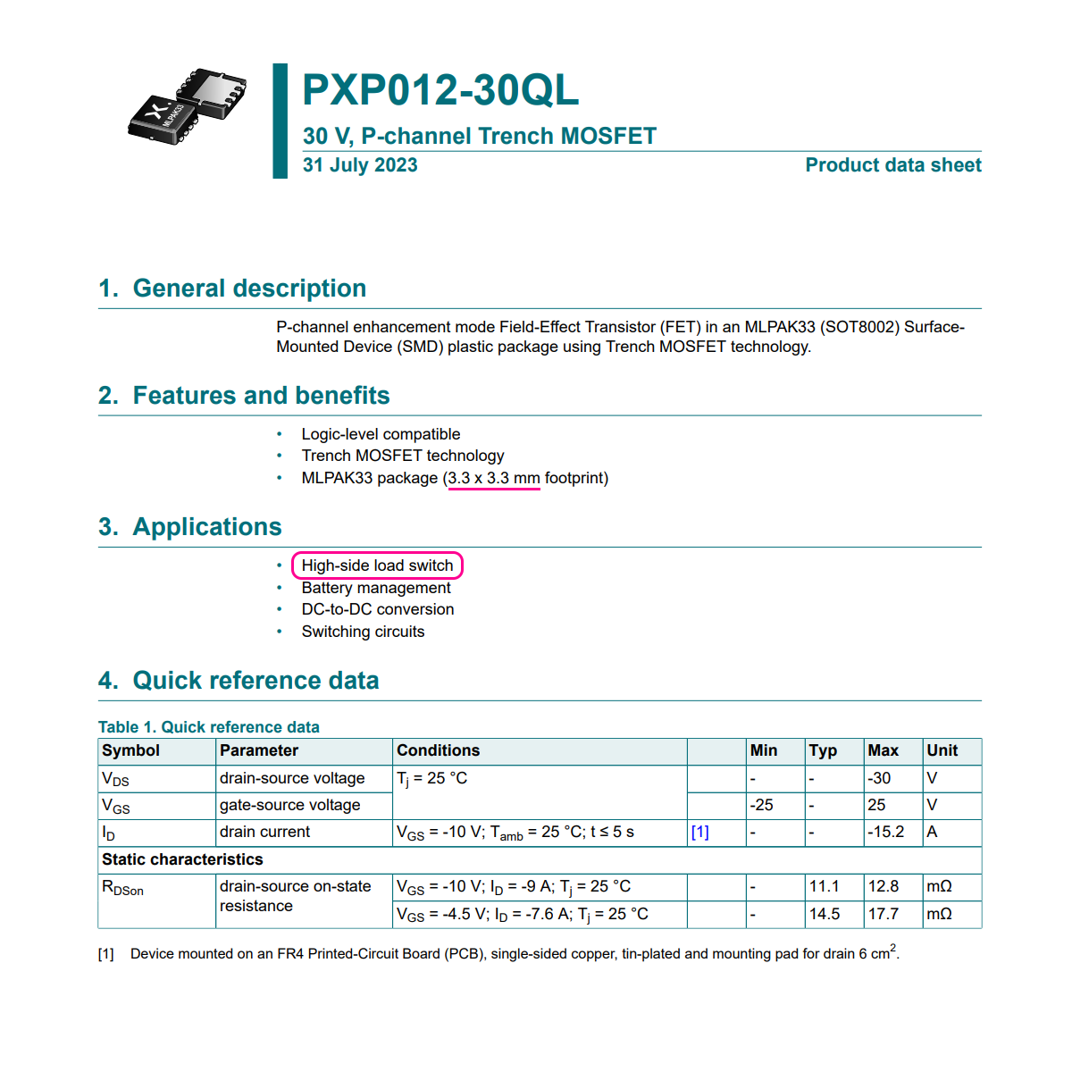
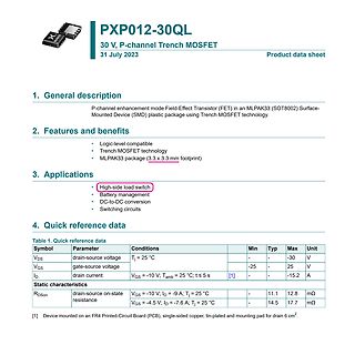
Datenblatt PXP012-30QL Trench MOSFET
PXP012-30QL 30 V, P-channel Trench MOSFET 31 July 2023 Product data sheet 1. General description P-channel enhancement mode Field-Effect Transistor (FET) in an MLPAK33 (SOT8002) Surface-Mounted Device (SMD) plastic package using Trench MOSFET technology. 2. Features and benefits Logic-level compatible Trench MOSFET technology MLPAK33 package (3.3 x 3.3 mm footprint) 3. Applications High-side load switch Battery management DC-to-DC conversion Switching circuits 4. Quick reference data Symbol Parameter Conditions
in „12V 2A per Raspberry Pi (3,3V) schalten“ · Analoge Elektronik und Schaltungstechnik · · Screenshots
-
PDF
IRLML6401.pdf
IRLML6401PbF l Ultra Low On-Resistance HEXFET Power MOSFET l P-Channel MOSFET l SOT-23 Footprint G 1 l Low Profile (<1.1mm) l Available in Tape and Reel V DSS = -12V 3 D l Fast Switching l 1.8V Gate Rated S 2 R DS(on) = 0.05Ω l Lead-Free l RoHS Compliant,
in „3,3 V schalten mit möglichgst geringem Spannungsabfall“ · Analoge Elektronik und Schaltungstechnik ·
-
PDF
Infineon-IRLIB9343-DS-v01_02-EN.pdf
IRLIB9343PbF ® HEXFET Power MOSFET Features Key Parameters VDS -55 V Advanced Process Technology Key Parameters Optimized for Class-D Audio Amplifier RDS(ON)typ. @ VGS=-10V 93 m Applications Low R for Improved Efficiency RDS(
in „DS3231 RTC Modul, Raspberry Pi, Zeitschaltung“ · Mikrocontroller und Digitale Elektronik ·
-
PDF
670135-DS01-1.pdf
property of its owner. IRFP450 Data Sheet January 2002 14A, 500V, 0.400 Ohm, N-Channel Features Power MOSFET • 14A, 500V This N-Channel enhancement mode silicon gate power field • r = 0.400Ω effect transistor is an advanced power MOSFET designed, DS(ON) • Single Pulse Avalanche Energy Rated tested, and guaranteed
in „Suche IRFP 450B“ · Markt ·
-
PDF
NCP1605-D.PDF
totem pole gate drive (+0.5/−0.8 A) makes it suitable to effectively drive high gate charge power MOSFETs. 11 V CC This pin is the positive supply of the IC. The circuit starts to operate whenCC exceeds 15 V (10.5 V for NCP1605A) and turns off when V CC goes below 9 V (typical values). After startup,
in „Hilfe bei der Reparatur eines Schaltnetzteiles erbeten“ · Analoge Elektronik und Schaltungstechnik ·
-
PDF
SI7611.pdf
New Product Si7611DN Vishay Siliconix P-Channel 40-V (D-S) MOSFET FEATURES PRODUCT SUMMARY V (V) R (Ω) I (A) Q (Typ.) • Halogen-free DS DS(on) D g TrenchFET Power MOSFET e 0.025 at VGS = - 10 V - 18 Low Thermal Resistance PowerPAK ® RoHS - 40 e 41 nC Package with
in „gleichwertiger Ersatztyp für Mosfet gesucht“ · Analoge Elektronik und Schaltungstechnik ·
-
PDF
UBA2000.pdf
exceeds its limit prot), the switching device will be turned off. During charge the gate of the MOSFET. As a result, the MOSFET the first few periods of conduction, the current protection is will be activated. disabled (disable time t ) to ensure that transient currents d To keep the MOSFET conductive
in „Schnellstarter für Leuchtstofföhren - welche taugen was?“ · Haus & Smart Home ·
-
PDF
post1.pdf
D4 D3 +12V P0D401 P0D402 P0D302 P0D301 0 0 Q Q P P R6 R3 P0R601 P0R602 0 MOSFET-P P0Q302 Q3 Q2 MOP0Q202 0 P0R301 1P0R302 1 1 0 0 P 0 0 P 1K 0 C14 Q Q 0 C18 1 P P 1 0 0 P P0L101 P0L100 P 100pF Q Q 100pF P P R8 R9 1K 0 MOSFET-N Q5 Q4 MOSFET-N 0 1K P0R801 P0R802 1 P0Q502 P0Q402 2
in „Vermeiden von Shoot Through in einer H-Bruecke“ · Mikrocontroller und Digitale Elektronik ·
-
PDF
recommended.pdf
Undervoltage lockout hysteresis 250 300 mV POWER SWITCH V I 5.4 V; O = 350 mA 165 250 DS(ON) P-channel MOSFET on-resistance V I 3.5 V; O = 200 mA 340 m V I 3 V; O = 100 mA 490 P-channel MOSFET leakage current VDS = 17 V 0.1 1 µA P-channel MOSFET current limit V I 7.2 V, VO= 3.3 V 2400 mA V I 5.4 V; O = 350 mA 145 200 r N-channel MOSFET on-resistance V = 3.5 V; I = 200 mA 170 m DS(ON) I O V I 3 V; O = 100 mA 200 N-channel MOSFET leakage V = 17 V 0.1 2 µA current DS POWER GOOD OUTPUT , LBI, LBO V Power good trip voltage V - V (PG)
in „Kurz vorm Verzweifeln“ · Analoge Elektronik und Schaltungstechnik ·
-
PDF
TPS6211.pdf
Undervoltage lockout hysteresis 250 300 mV POWER SWITCH V I 5.4 V; O = 350 mA 165 250 DS(ON) P-channel MOSFET on-resistance V I 3.5 V; O = 200 mA 340 m V I 3 V; O = 100 mA 490 P-channel MOSFET leakage current VDS = 17 V 0.1 1 µA P-channel MOSFET current limit V I 7.2 V, VO= 3.3 V 2400 mA V I 5.4 V; O = 350 mA 145 200 r N-channel MOSFET on-resistance V = 3.5 V; I = 200 mA 170 m DS(ON) I O V I 3 V; O = 100 mA 200 N-channel MOSFET leakage V = 17 V 0.1 2 µA current DS POWER GOOD OUTPUT , LBI, LBO V Power good trip voltage V - V (PG)
in „DC DC Wandler Pins“ · Analoge Elektronik und Schaltungstechnik ·
-
PDF
TPS6211.pdf
Undervoltage lockout hysteresis 250 300 mV POWER SWITCH V I 5.4 V; O = 350 mA 165 250 DS(ON) P-channel MOSFET on-resistance V I 3.5 V; O = 200 mA 340 m V I 3 V; O = 100 mA 490 P-channel MOSFET leakage current VDS = 17 V 0.1 1 µA P-channel MOSFET current limit V I 7.2 V, VO= 3.3 V 2400 mA V I 5.4 V; O = 350 mA 145 200 r N-channel MOSFET on-resistance V = 3.5 V; I = 200 mA 170 m DS(ON) I O V I 3 V; O = 100 mA 200 N-channel MOSFET leakage V = 17 V 0.1 2 µA current DS POWER GOOD OUTPUT , LBI, LBO V Power good trip voltage V - V (PG)
in „QFN Gehäuse.“ · Analoge Elektronik und Schaltungstechnik ·
-
PDF
TPS6211.pdf
Undervoltage lockout hysteresis 250 300 mV POWER SWITCH V I 5.4 V; O = 350 mA 165 250 DS(ON) P-channel MOSFET on-resistance V I 3.5 V; O = 200 mA 340 m V I 3 V; O = 100 mA 490 P-channel MOSFET leakage current VDS = 17 V 0.1 1 µA P-channel MOSFET current limit V I 7.2 V, VO= 3.3 V 2400 mA V I 5.4 V; O = 350 mA 145 200 r N-channel MOSFET on-resistance V = 3.5 V; I = 200 mA 170 m DS(ON) I O V I 3 V; O = 100 mA 200 N-channel MOSFET leakage V = 17 V 0.1 2 µA current DS POWER GOOD OUTPUT , LBI, LBO V Power good trip voltage V - V (PG)
in „Trennung von analoger und digitaler Spannung“ · Analoge Elektronik und Schaltungstechnik ·
-
PDF
tps54525.pdf
..................5 • Changed the Over/Under Voltage Protection section. From: "as the high-side MOSFET driver turns off and the low-side MOSFET turns on" To: "as both the high-side and low-side MOSFET drivers turn off"............... 12 2 Submit Document Feedback Copyright © 2021 Texas Instruments Incorporated
in „TPS54525 wandelt erst nach Kurzschluss EN zu PGOOD“ · Analoge Elektronik und Schaltungstechnik ·