-
PDF
DFUE-1-6.pdf
db 00h ; ;--------------------------------------------------------------- ; Bufferbereich ; oldio: ds 1h ; Sicherung Io-Byte dstbeg ds 2 ; dstend ds 2 ; bzaehl db 0 ; Sicherung fuer Zaehlregister (B) buflaeng ds 2 ; Bufferlaenge recz ds 1 ; Recordzaehler asciih db 30h ; ASCII "0" asciil db 30h ; ASCII
in „Suche MOPPEL Projekt in Heft oder .PDF“ · Mikrocontroller und Digitale Elektronik ·
-
PDF
L6206.pdf
18 GND INA 11 26 INB SENSEA 12 25 SENSEB OUT1 B 8 17 VSB OCD A 13 24 OCD B OCD B 9 16 OUT2 B N.C. 14 23 N.C. SENSE 10 15 VBOOT B OUT1A 15 22 OUT1B IN1B 11 14 ENB N.C. 16 21 N.C. IN2B 12 13 PROGCL B N.C. 17 20 N.C. GND 18 19 GND D99IN1089A D99IN1090A (1) PowerDIP24/SO24 PowerSO36 1. The slug is internally
in „l6206 Datenblatt Fehler?“ · Mikrocontroller und Digitale Elektronik ·
-
PDF
z16c30um.pdf
within a 16-bit trans- fer of serial data, and apply to DMA and processor ac- cesses to RDR and TDR. 2-14 UM97USC0100 Z16C30USC® USERSM ANUAL ZILOG ADnn Address Data A//B, D//C /CS /SITACK /PITACK,/WR,(/RD OR /DS), DMAAcknowledge signals /AS (Required with /DS, not with /RD.) R//W /DS or /RD Wait Mode /WAIT
in „unbekanntes Bus (Frame) entziffern, brauche Hilfe.“ · Mikrocontroller und Digitale Elektronik ·
-
Datei
0217b-DS10-SD-sektor_auslesen-als_antwort_senden.c
********** // * Datenspeicher 10 * // ******************* // Flüssigkristallanzeige LMK62R125A1 // DS18B20 NR. 13,14,15,16 an 63-10 Adresse 0x18 // E32-868TD Funk ab 29.8.21 //Änderungen: /************************************************************************/ // MSP430F1611 // ----------------- //
in „512 Byte-Sektor einer SD-Karte mit E32-868T drahtlos übertragen“ · Mikrocontroller und Digitale Elektronik ·
-
PDF
Disketten_Info.pdf
Motorsteuereingang (Leitung 16). In modernen Laufwerken sind meist nur die Laufwerksauswahleingänge DS0 und DS1 angeschaltet (Leitungen 10, 12); die Auswahlsignale DS2, 3 (Leitungen 14, 6) werden nicht ausgewertet. Abb. 1.7 Die Anschlüsse an marktüblichen Laufwerken (Beispiele; Ansicht von hinten in normaler
in „Floppy FDD Diskette an AVR Mikrocontroller ATmega Beispiele Assembler“ · Projekte & Code ·
-
Datei
AT32MENU_Int_anzeige_Abfrage_Passwort.bas
Echtzeituhr Ddrd = &HFE Ddrb.1 = 1 Config Sda = Portc.1 ' I2C Bus konfigurieren Config Scl = Portc.0 Const Ds1307w = &HD0 ' Addresse der Ds1307 Uhr Const Ds1307r = &HD1 Config Clock = User '' Interne Time/Date Routinen für Bascom konfigurieren Config Date = Dmy , Separator = . ' *********** Konfiguration Ende
in „Servomotor ansteuern in Bascom“ · Mikrocontroller und Digitale Elektronik ·
-
PDF
TMC4671-LA_datasheet.pdf
TMC4671 Datasheet • IC Version V1.3 | Document Revision V2.08 • 2022-July-26 107 / 153 0: off 1: on GPIO_dsADCI_CONFIG[1] bit(1) SEL_nGPIO_dsADCS_A 0: off 1: on GPIO_dsADCI_CONFIG[2] bit(2) SEL_nGPIO_dsADCS_B 0: off 1: on GPIO_dsADCI_CONFIG[3] bit(3) SEL_GPIO_GROUP_A_nIN_OUT 0: off 1: on GPIO_dsADCI_CONFIG[4]
-
PDF
AG101.pdf
Operational Bandwidth MHz 60 3000 Frequency MHz 900 1900 900 1900 Test Frequency MHz 800 S21 (5) dB 14 12.8 14 12.5 Gain dB 13 14 16 S11 dB -10 -9 -10 -9 Input Return Loss(5) dB 8.5 S22 dB -27 -22 -28 -19 Output Return Loss dB 20 Output P1dB dBm +15 +15 +14 +14 Output P1dB dBm +15 Output IP3 dBm +32.5
-
PDF
BTS780.pdf
GND 4 GH1 5 Heat-Slug 2 ST1 6 SH1 7 DHVS 8 17 DHVS GND 9 GH2 10 ST2 11 SH2 12 Heat-Slug 3 SL2 13 SL2 14 16 DL2 GL2 15 AEP02224 Figure 1 Pin Configuration (top view) Data Sheet 3 1999-06-22 BTS 780 GP Pin Definitions and Functions Pin No. Symbol Function 1, 2 SL1 Source of low-side switch 1 3 GL1 Gate of
in „BTS780GP Motortreiber“ · Analoge Elektronik und Schaltungstechnik ·
-
Datei
read_rtc_temp.c
#define DS1307_ID 0x68 // wie DS3231 // diese CONTROL_REGISTER sind für DS3231, bitte anpassen für DS1307 -> Datenblatt // BIT 7 BIT 6 BIT 5 BIT 4 BIT 3 BIT 2 BIT 1 BIT 0 #define CONTROL_REGISTER 0x0E // 14d NAME
in „RTC DS1307 1Hz“ · Mikrocontroller und Digitale Elektronik ·
-
PDF
NHD-0420CW-AY3-587980.pdf
2 for details Display-dot DH’ = "1": display shift enable DH’ = "0": dot scroll enable (POR) Shift DS[4:1]=1111b (POR) when DH’ = 1b Determine the line for display shift. DS1 = "1/0": 1st line display shift enable/disable Shift Enable 1 1 0 0 0 0 0 0 1 DS4 DS3 DS2 DS1 DS2 = "1/0": 2nd line display shift enable/disable DS3 = "1/0": 3rd line display shift enable/disable DS4 = "1/0": 4th line display shift enable/disable. HS[4:1]=1111b (POR) when DH’ = 0b Determine the line for horizontal smooth scroll. HS1 = "1/0": 1st
in „NHD-0420CW-AY3 4x20 Zeilen OLED in Betrieb nehmen“ · Mikrocontroller und Digitale Elektronik ·
-
PDF
SBR10U40CTFP.pdf
, SBR10U40CTFP April 2015 Document number: DS30951 Rev. 8 - 2 www.diodes.com © Diodes Incorporated SBR10U40CT, SBR10U40CTFP Package Outline Dimensions (cont.) Please see AP02002 at http://www.diodes.com/datasheets/ap02002.pdf for the latest version
in „Aufwärtsschaltregler bauen“ · Analoge Elektronik und Schaltungstechnik ·
-
PDF
DAC014N120Z5.pdf
Mode MOSFET Features VDSS 1200V ವ▯+LJK▯EORFNLQJ▯YROWDJH ID(@25ഒ) 135A ವ▯+LJK▯IUHTXHQF\▯RSHUDWLRQ R DS(ON) 14mΩ ವ▯/RZ▯RQ▯UHVLVWDQFH ವ▯)DVW▯LQWULQVLF▯GLRGH▯ZLWK▯ORZ▯UHYHUVH▯UHFRYHU\ TO-247-4L ವ▯▯▯▯▯▯$YDODQFKH▯WHVWHG Benefits ▯ ವ▯+LJKHU▯V\VWHP▯HIILFLHQF\ ▯ ▯ ▯ ವ▯+LJK▯WHPSHUDWXUH▯DSSOLFDWLRQ ವ▯+DUG▯VZLWFKLQJ
in „Doppelter Sourceanschluss bei SiC-Mosfets“ · Analoge Elektronik und Schaltungstechnik ·
-
PDF
HAP-CU-TechDok-20080319.pdf
Bit 7 Bit 6 Bit 5 Bit 4 Bit 3 Bit 2 Bit 1 Bit 0 LByte 3 2 1 0 -1 -2 -3 -4 2 2 2 2 2 2 2 2 Bit 15 Bit 14 Bit 13 Bit 12 Bit 11 Bit 10 Bit 9 Bit 8 HByte S S S S S 2 6 25 24 Abb. 4.4: Werteformat beim digitalen Thermometer (DS18B20) Die nachfolgende Tabelle gibt einige Temperaturwerte und deren zugehöriges
-
PDF
DS3231_M_MZ_Mems.pdf
100 200 300 400 TEMPERATURE (°C) SCL FREQUENCY (kHz) Maxim Integrated │ 6 www.maximintegrated.com 2 DS3231M ±5ppm, I C Real-Time Clock Pin Configuration TOP VIEW 32KHZ 1 + 16 SCL TOP VIEW VCC 2 15 SDA 32KHZ 1 + 8 SCL INT/SQW 3 DS3231M 14 VBAT V 2 7 SDA RST 4 13 GND CC DS3231M N.C. 5 12 N.C. INT/SQW 3
in „(empfindlicher) GPS Modul gesucht“ · Mikrocontroller und Digitale Elektronik ·
-
PDF
93LC66.pdf
not exceed .005" (0.127mm) per side. JEITA (formerly EIAJ) equivalent: SC-74A Drawing No. C04-120 DS21795A-page 14 2003 Microchip Technology Inc. 93AA66A/B/C, 93LC66A/B/C, 93C66A/B/C 8-Lead Plastic Dual In-line (P) – 300 mil (PDIP) E1 D 2 n 1 α E A A2 L c A1 β B1 p eB B Units INCHES* MILLIMETERS Dimension
-
PDF
DMP10H400SEQ-838150.pdf
Voltage Drain Current DSS 1 µA VDS = -80V, GS= 0V Gate-Source Leakage GSS ±100 nA VGS = ±20V, DS = 0V ON CHARACTERISTICS (Note 7) Gate Threshold Voltage V -1.0 -2.2 -3.0 V V = V , I = -250µA GS(TH) DS GS D 203 250 VGS = -10V,DI = -5A Static Drain-Source On-Resistance R DS(ON) 241 300 m VGS
in „Externe Festplatte durch falsches Netzteil zerstört“ · PC Hard- und Software ·
-
PDF
TC2014.pdf
EIAJ Equivalent: SC-74A Drawing No. C04-091 Revised 09-12-05 2001-2012 Microchip Technology Inc. DS21662F-page 13 TC2014/2015/2185 NOTES: DS21662F-page 14 2001-2012 Microchip Technology Inc. TC2014/2015/2185 APPENDIX A: REVISION HISTORY Revision F (December 2012) • Added a note to each package outline
in „Mcp3551 PT1000 Schaltung“ · Mikrocontroller und Digitale Elektronik ·
-
Datei
Devices.txt
TP06SQ 14 RES10 14 QG5860 14 MA04-2 14 MA04-1 14 L-EU0204/5 14 IRFP240 14 CPOL-EU153CLV-0405 14 C1206 13 NC 13 LEDCHIP-LED0805 13 JP1Q 13 IRF540 13 HD-H103 13 ELC-5 13 CRYSTALHC49U70 13 CPOL-EUSMCC 13 CPOL-EUB45181A
in „[KiCad] Bibliotheksaufbau - Konzeptideen gesucht“ · Platinen ·
-
PDF
HEIZUNG_UNGARN.PDF
P IJ 80 3 R13 27R P IJ 80 4 PI10 PI10 C12 100nF PC21 PI10 P5PI 6 O1 P0 C13 100nF R21 PC31 PI10 P1 R14 470R C14 100nF 10k C11 100nF P0 PC41 PI10 PI10 PC10 P1 3 3 2 131 U4 B P1 C10 100nF B R15 PI0 6 C C C O I 25 15K R16 PI10 PC10 PI U40 6 3V3OUT V V V / C TXD P IU402 5 RXD_MC 1K5 A C RXD P IU402 4 TXD_MC
-
PDF
ureflow.pdf
1 2 3 4 5 6 D2 U3 +3V3 5VIN DS14W +5V +3V3 +3V3 VIN FB1 NCP1117 1 2 3 VI VO 2 VBUS D N C3 +3V3 U5 R12 R16 GND C2 G R8 R10 MAX6675ISA+T SW1 10K SW3 10K F1 D3 10uF 1 10uF 10K 1.5K A 500mA DS14W 4 1 4 BTN_LEFT 1 4 BTN_RIGHT A VCC 2 3
in „Feedback Schaltplan STM32G0“ · Mikrocontroller und Digitale Elektronik ·
-
PDF
gps-ms1e.pdf
module (on the PCB). See Figure 6 for the location of the temperature sensors on the module. GPS-MS-DS-ST-0132 Datasheet GPS-MS1E µ-blox ag, May 16, 2000 Page 14 Figure 6: Sensor Position GPS-MS-DS-ST-0132 Datasheet GPS-MS1E µ-blox ag, May 16, 2000 Page 15 9 Mechanical Specifications Figure 7 shows the
in „Aktive GPS Antenne mit 4,5 Volt wie Einspeisen?“ · Mikrocontroller und Digitale Elektronik ·
-
PDF
PI4IOE5V9555.pdf
Output 6 11 8 IO0_7 I/O Port 0 Input/Output 7 12 9 GND G Ground 13 10 IO1_0 I/O Port 1 Input/Output 0 14 11 IO1_1 I/O Port 1 Input/Output 1 15 12 IO1_2 I/O Port 1 Input/Output 2 16 13 IO1_3 I/O Port 1 Input/Output 3 17 14 IO1_4 I/O Port 1 Input/Output 4 18 15 IO1_5 I/O Port 1 Input/Output 5 19 16 IO1_6
in „Schachbrettposition Erkennung“ · Mikrocontroller und Digitale Elektronik ·
-
PDF
NDT455N.pdf
Drain-SourceBreakdownVoltage V = 0 V, I = 250 µA 30 V DSS GS D I ZeroGateVoltage DrainCurrent V = 24 V, V = 0 V 1 µA DSS DS GS T = 55°C 10 µA J I Gate-BodyLeakage,Forward V = 20 V, V = 0 V 100 nA GSSF GS DS I Gate-BodyLeakage,Reverse V = -20 V, V = 0 V -100 nA GSSR GS DS ON CHARACTERISTICS (Note2) V GateThresholdVoltage V
in „Fairchild 918 455 -> Ersatz?“ · Analoge Elektronik und Schaltungstechnik ·
-
PDF
BTS_100_High_Side.pdf
0, D = — 0.25 mA — 50 — — Gate threshold voltage V GS(th) V = V , I = — 1 mA — 2.5 — 3.0 — 3.5 GS DS D Zero gate voltage drain current I DSS A V = 0 V,V = — 50 V GS DS Tj= 25 °C — — 1 — 10 Tj= 150 °C — — 100 — 300 Gate-source leakage current I GSS VGS = — 20 V,V DS= 0 Tj= 25 °C — — 10 — 100 nA Tj= 150
in „Motorsteuerung mit kollektorschaltung“ · Mikrocontroller und Digitale Elektronik ·
-
PDF
bts100.pdf
0, D = — 0.25 mA — 50 — — Gate threshold voltage V GS(th) V = V , I = — 1 mA — 2.5 — 3.0 — 3.5 GS DS D Zero gate voltage drain current I DSS A V = 0 V,V = — 50 V GS DS Tj= 25 °C — — 1 — 10 Tj= 150 °C — — 100 — 300 Gate-source leakage current I GSS VGS = — 20 V,V DS= 0 Tj= 25 °C — — 10 — 100 nA Tj= 150
in „BTS 100 Ersastzlösung“ · Mikrocontroller und Digitale Elektronik ·
-
 Bild
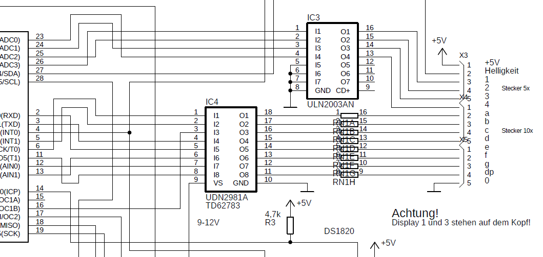
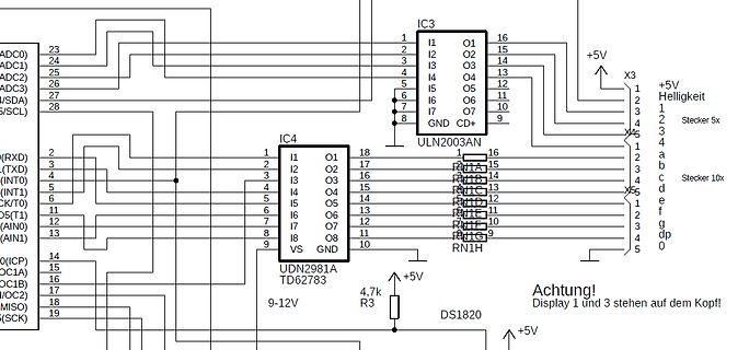
Schaltplan mit ICs und Anschlüssen
ADC0) 23 ADC1) 24 ADC2) 25 ADC3) 26 I2C/SDA) 27 SCL/SCK) 28 (RXD) 2 (TXD) 3 (INT0) 4 (INT1) 5 DS(T1) 11 (AIN0) 12 (AIN1) 13 OC(ICP) 14 OC1A) 15 OC1B) 16 MISO) 18 (SCK) 19 IC3 1 I1 16 O1 2 I2 15 O2 3 I3 14 O3 4 I4 13 O4 5 I5 12 O5 6 I6 11 O6 7 I7 10 O7 8 GND CD+ IC4 1 I1 18 O1 2 I2 17 O2 3 I3 16 O3 4 I4 15 O4 5 I5 14 O5 6 I6 13 O6 7 I7 12 O7 8 I8 11 O8 9 VS GND 10 ULN2003AN 16 R1A 15 R1B 14 R1C 13 R1D 12 R1E 11 R1F 10 R1G 9 RN1H +5V X3 +5V Helligkeit 1 Stecker 5x 2 3 4 c Stecker 10x d e f g dp 4,7k R3 9-12V DS1820
in „LEDs mit gemeinsamen GND schalten“ · Analoge Elektronik und Schaltungstechnik · · Schaltpläne
-
PDF
LiveDesign_Schematics.pdf
Sheet2 of 10 Australia 2086 File:NEB_XTALOSC.SchDoc 1 2 3 4 1 2 3 4 5 6 6 DIGIT 7-SEGMENT DISPLAY A DS1 DS2 DS3 DS4 A DIG0_SEG0 R25 270R 7 3 DIG1_SEG0 R26 270R 7 3 DIG2_SEG0 R27 270R 7 3 DIG3_SEG0 R28 270R 7 3 DIG0_SEG1 R29 270R 6 a K 8 DIG1_SEG1 R30 270R 6 a K 8 DIG2_SEG1 R31 270R 6 a K 8 DIG3_SEG1 R32
-
Datei
20130919Schiebe595out597in.c
liegen bei Master :(SCK (Takt), MISO (In), MOSI (Out)) #define DD_MOSI DDB5 // MOSI Breitband PIN 14, 595er DS = SER = MOSI, 595er PIN 14 #define DD_MISO DDB6 // MISO Breitband PIN 15, 597er DS = SER = MISO, 597er PIN 14 #define DD_SCK DDB7 // Breitband Pin 16 auf SCK = SHCP IC Pin 11, fuer 595 und 597, sorgt für den Flankenwechsel #define DD_SS_o DDB4 // Breitband Pin 13 RCK = STCP IC PIN 14 fuer output 595er (kopiere das Ausgangsregister) #define DD_SS_i DDC1 // Breitband Pin 18 RCK = STCP IC PIN 14 fuer input 597er (lese das Eingangsregister) #define DD_p597 DDC7 // Parallel Load Shift
in „Problem Schieberegister 595er ud 597er“ · Mikrocontroller und Digitale Elektronik ·
-
PDF
catalog-3.pdf
14-SOIC MPN: OPA4344PA [ID]: 000127 [Price]: 1.9016 USD [QTY]: 5 [Category]: Amplifiers - Op Amps, Buffer, Instrumentation [Desc]: Operational Amplifier, 1 Mhz, 4, 0.8 V/ S, 2.5V To 5.5V, Dip, 14 Rohs Compliant
-
 Bild
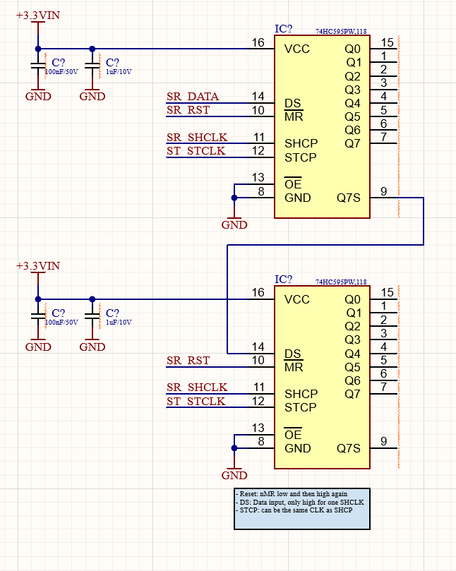
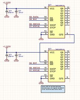
Schaltplan mit zwei 74HC595 Schieberegistern
+3.3VIN C? 100nF/50V GND C? 1uF/10V GND SR DATA 14 IC? 74HC595PW,118 16 VCC 15 Q0 1 Q1 2 Q2 3 Q3 4 Q4 5 Q5 6 Q6 7 Q7 10 DS 4 MR 5 Q4 11 SHCP 6 Q5 12 STCLK 7 Q6 13 OE 8 GND 9 Q7S SR RST SR SHCLK STCLK +3.3VIN C? 100nF/50V GND C? 1uF/10V GND SR RST 14 IC? 74HC595PW,118 16 VCC 15 Q0 1 Q1 2 Q2 3 Q3 4 Q4 5 Q5 6 Q6 7 Q7 10 DS 4 MR 5 Q4 11 SHCP 6 Q5 12 STCLK 7 Q6 13 OE 8 GND 9 Q7S SR RST SR SHCLK STCLK GND - Reset: nMR low and then high again - DS: Data input, only high for one SHCLK - STCP: can be the same CLK as SHCP
in „32-bit Shift-Counter“ · Mikrocontroller und Digitale Elektronik · · Schaltpläne
-
PDF
LiveDesign_EB_Schematics-xilinx_spartan.pdf
Sheet 2 of10 Australia 2086 File: NEB_XTALOSC.SchDoc 1 2 3 4 1 2 3 4 5 6 6 DIGIT 7-SEGMENT DISPLAY A DS1 DS2 DS3 DS4 A DIG0_SEG0 R25 270R 7 a K 3 DIG1_SEG0 R26 270R 7 a K 3 DIG2_SEG0 R27 270R 7 a K 3 DIG3_SEG0 R28 270R 7 a K 3 DIG0_SEG1 R29 270R 6 8 DIG1_SEG1 R30 270R 6 8 DIG2_SEG1 R31 270R 6 8 DIG3_SEG1
-
Datei
AssemblerApplication7.asm
def null = r5 .def accu = r16 .def index = r17 .def onewireindex = r20 .def rawlow = r24 ;Rohwerte DS18x20 .def rawhigh = r25 .equ DQ = 7 ;Datenleitung des Ds18x20 .equ DS_DDR = DDRB .equ DS_Port = PortB .equ DS_Pin = PinB .equ LCD = PortD .equ LCDDDR = DDRD .equ LCMD = PortA .equ LCMDDR = DDRA .equ
in „wieder ein DS18B20 Problem“ · Mikrocontroller und Digitale Elektronik ·
-
PDF
uC51_UEdit_T_Deck_s.pdf
Command Line Arguments = Category&02 = COMPILER OPTIONS Processor = Intel MCS51 (8051-family)|Dallas DS80C390|Dallas DS80C400|Freescale/Motorola HC08|Zilog Z80|GameBoy Z80|Atmel AVR|Microchip PIC 14- bit (p16f84-family)|Microchip PIC 16-bit (p18f452-family)|Toshiba TLCS-900H|Phillips XA51 Compiler Options
in „Wickenhäuser uC51 und UltraEdit“ · Mikrocontroller und Digitale Elektronik ·
-
PDF
BST-BMP180-DS000-09-2.pdf
BMP180 Data sheet Document revision 2.5 Document release date 5 April 2013 Document number BST-BMP180-DS000-09 Technical reference code(s) 0 273 300 244 Notes Data in this document are subject to change without notice. Product photos and pictures are for illustration purposes only and may differ from the
in „BMP180 Luftdruck Sensor“ · Mikrocontroller und Digitale Elektronik ·
-
PDF
Halbleiterliste.pdf
2SK30A 1 Mosfet 4049BCD 4 Hex Inverting Buffer https://pdf.datasheetcatalog.com/datasheets/70/109093_DS.pdf 4085PC 4 CMOS Dual 2-wide 2-input and-or-invert gate https://www.ti.com/lit/ds/symlink/cd4085b.pdf 4520BPC 2 Dual 4 bit binary counter https://datasheetspdf.com/pdf-file/504568/FairchildSemiconductor
-
PDF
S2-L2-5V.pdf
mH power, voltage, mW V DC (40 °C) ST-L1-3V 3 2.1 0.3 33 90 0.04 99 8.4 ST-L1-5V 5 3.5 0.5 16 300 0.14 80 15.3 ST-L1-6V 6 4.2 0.6 16 360 0.14 96 16.8 ST-L1-12V 12 8.4 1.2 8 1450 0.6 96 33.7 ST-L1-24V 24 16.8 2.4 4 5700 2.05 96 66.7 ST-L1-48V 48 33.6 4.8 3 16,000 8.9 144 111 2 coil latching Nominal Maximum
in „24V Relais ansteuern“ · Analoge Elektronik und Schaltungstechnik ·
-
PDF
S2-L2-5V.pdf
mH power, voltage, mW V DC (40 °C) ST-L1-3V 3 2.1 0.3 33 90 0.04 99 8.4 ST-L1-5V 5 3.5 0.5 16 300 0.14 80 15.3 ST-L1-6V 6 4.2 0.6 16 360 0.14 96 16.8 ST-L1-12V 12 8.4 1.2 8 1450 0.6 96 33.7 ST-L1-24V 24 16.8 2.4 4 5700 2.05 96 66.7 ST-L1-48V 48 33.6 4.8 3 16,000 8.9 144 111 2 coil latching Nominal Maximum
in „(V) 4-Fach 5*7 Punktmatrix Osram DLR 2416, Bistabile Relais SDS, LED-Display 7-Seg. 4-Fach“ · Markt ·
-
PDF
IRF_1404_S.pdf
Voltage (V) V DS , Drain-to-Source Voltage (V) Fig 7. Typical Source-Drain Diode Fig 8. Maximum Safe Operating Area Forward Voltage 4 www.irf.com IRF1404S/L R 200 V D LIMITED BY PACKAGE DS VGS 160 D.U.T. R G + A - DD
in „Geiger Counter Sparkfun“ · Mikrocontroller und Digitale Elektronik ·
-
PDF
gbdso_uk.pdf
D7 IC2 10 RD 11 10 15 INT DX 5V 2V5 100k 2V5 2 COUT 6 16 WR 22 15 0 0 1 RD K3 CW C8 NC RESET CS A0 14 0 2 WR 1 VB CLK 7 13 REF– A1 21 1 G 7 15 9 D1 13 2 2 3 A13 1 +5V D2 100n NC DQ 12 3 IC6 2 ECLK 5V 5V A SOUT 14 12 11 74HC138D 3 DS1267S100 4 WR C13 10 5 4 A14 4 RD BAV199 3 H1 L1 4 9 6 5 ECLK 5 RAM_CS
in „Bameboy-LCD mit avr“ · Mikrocontroller und Digitale Elektronik ·
-
PDF
gbdso_uk.pdf
D7 IC2 10 RD 11 10 15 INT DX 5V 2V5 100k 2V5 2 COUT 6 16 WR 22 15 0 0 1 RD K3 CW C8 NC RESET CS A0 14 0 2 WR 1 VB CLK 7 13 REF– A1 21 1 G 7 15 9 D1 13 2 2 3 A13 1 +5V D2 100n NC DQ 12 3 IC6 2 ECLK 5V 5V A SOUT 14 12 11 74HC138D 3 DS1267S100 4 WR C13 10 5 4 A14 4 RD BAV199 3 H1 L1 4 9 6 5 ECLK 5 RAM_CS
in „Alternative zu teurem Oszilloskop“ · Analoge Elektronik und Schaltungstechnik ·
-
PDF
Ferritperlen.pdf
Capacitance Ferrite Dimensions Insertion W.V. T.C. Beads Loss –25°C to +85°C FOR GENERAL APPLICATIONS DS310-55Y5S271M100 270pF ± 20% 100V DS310-55Y5S222M100 2200pF ± 20% 100V ±22% None Fig. 1 Fig. 4 DS310-55Y5S223S50 22000pF + 50%, –20% 50V DS310-55Y5S104M16 100000pF ± 20% 16V DST310-55Y5S271M100 270pF
in „24Bit Delta-Sigma ADC-Eingang vor ESD und Überspannung schützen“ · Analoge Elektronik und Schaltungstechnik ·
-
PDF
MCP1802.pdf
between the input source voltage and the input capacitance of the LDO. 2010 Microchip Technology Inc. DS22053C-page 13 MCP1802 MCP1802 +V IN V IN VOUT +V SHDN Shutdown IN Control Voltage - Reference + Current Limiter Error Amplifier GND FIGURE 4-1: Block Diagram. DS22053C-page 14 2010 Microchip Technology
in „Spannungsregler LDO - Ausgangs-Spannung schaltet nicht 100% ab“ · Analoge Elektronik und Schaltungstechnik ·
-
PDF
MCP1801.pdf
between the input source voltage and the input capacitance of the LDO. 2010 Microchip Technology Inc. DS22051D-page 13 MCP1801 MCP1801 +VIN V IN VOUT +V IN SHDN Shutdown Voltage Control Reference - + Current Limiter Error Amplifier GND FIGURE 4-1: Block Diagram. DS22051D-page 14 2010 Microchip Technology
in „USB-Spannungsversorgung lässt PIC24FJ128 abstürzen?“ · Mikrocontroller und Digitale Elektronik ·
-
Datei
owaf.c
; } void OneWire_Write1_atOnce(void) { OneWire_LowLevel(); _delay_us(C_SHORT_PULSE_US); /* 3,5µs = 14 * 4 * tick(=62,5ns) */ /* 1,5µs = 6 * 4 * tick(=62,5ns) */ uint8_t u8_Delay = 0; for(u8_Delay = 0; u8_Delay < 14; u8_Delay++) { asm(";wait"); } OneWire_HighLevel(); /* 60µs = 8 * 120 * 62,5ns */ OCR0
in „1 Wire manche Teilnehmer antworten nicht“ · Mikrocontroller und Digitale Elektronik ·
-
PDF
AN2662-Sensorless-Drive-forSingle-and-Two-PhaseBLDC-Motor-00002662A.pdf
implement an intelligent motor stall detection. © 2018 Microchip Technology Inc. Application Note DS00002662A-page 14 AN2662 Revision History 8. Revision History Doc Rev. Date Comments A 09/2018 Initial document release. © 2018 Microchip Technology Inc. Application Note DS00002662A-page 15 AN2662 APPENDIX
in „EBM-Papst EC Motor“ · Analoge Elektronik und Schaltungstechnik ·
-
PDF
tca8418.pdf
A N/A N/A N/A C9IS C8IS 0x13 GPIO_INT_STAT3 GPIO interrupt status 0 0 0 0 0 0 0 0 GPIO_DAT_STAT1 0x14 (read twice to clear) GPIO data status R7DS R6DS R5DS R4DS R3DS R2DS R1DS R0DS 0x15 GPIO_DAT_STAT2 GPIO data status C7DS C6DS C5DS C4DS C3DS C2DS C1DS C0DS (read twice to clear) 0x16 GPIO_DAT_STAT3 GPIO
in „Keypad 3x4 (am Tasmota o.ä.)“ · Mikrocontroller und Digitale Elektronik ·
-
PDF
p75nf75.pdf
0.0095Ω- 80A - TO-220 - TO-220FP - D PAK STripFET™ II Power MOSFET General features Type V R I DSS DS(on) D STB75NF75 75V <0.011Ω 80A (1) (1) 3 3 STP75NF75 75V <0.011Ω 80A 1 2 1 2 STP75NF75FP 75V <0.011Ω 80A (1) TO-220 TO-220FP 1. Current limited by package ■ Exceptional dv/dt capability ■ 100% avalanche
in „Unbekanntes Bauteil im Akkuschrauber“ · Analoge Elektronik und Schaltungstechnik ·
-
PDF
CY3272_Schematic.pdf
R8 GND LOG_ADDTXR_S0HUTDOWN TXDISABLE 330 19 RESET TXDISABLE MTG4 DIP Switch 5 Position TX_LED 16 DS3 11 I2C_SDA RX_LED 1 RESET VDD VDD 10 I2C_SCL BIU_LED 18 Tx GND S2 GND HOST_INT 23 3 1 DS2 4 2 14 22 GRN GND R6 R7 Vss AGND Rx R3 VDD 7.50k 7.50k CY8CPLC10 DS4 1.00k RED BIU R1 I2C J3 GND 1.00k 1 C6
in „Power Line bzw. Power LAN im Selbstbau“ · Haus & Smart Home ·