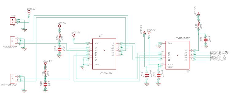
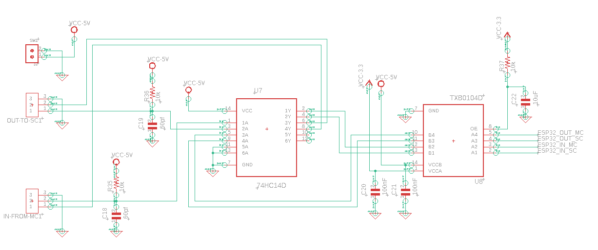
, Du willst per Hand löten? Da gibt es vielleicht andere, die im SOIC Gehäuse zu finden sind (z.B. TXB0104). 2 MBit/s könnte auch noch mit einem Spannungsteiler funktionieren (siehe SD-Karten Anbindung z.B. von Ulrich Radig).
Devices AD7682 Stepperdriver TI TLC5916 l ah ba m d 35c a bel be dk 4 ban c lch m F e m ter 5 bah hn TI TXB0104 SD Card n5 b cm t 5cm ei ban L eier L AVATAtEGeAg2a5265060
Vielen Dank ! ich hatte schon gehofft 8 MHz per SPI nutzen zu können. Momentan hatte ich an einen TXB0104 als Pegelwandler gedacht, nur ist der eben auch in SMD. Das passt nicht so leicht auf ein Steckbrett.
Portexpander (funktioniert) - Display1 (funktioniert) - Display2 (funktioniert) | Levelshifter TXB0104 | - 1 kOhm Pull-Up | - LM75 Auf LM75 Seite: 4,26 V VCC 1,75 V bzw. 1,74 V wenn er hängt 0,67 V wenn ich die Datenleitung abziehe µC hört auf zu senden (mit LEDs an Leitung getestet)
einige Level Shifter IC's: - SN74LVC8T245 - SN74LVC2T45 - MAX3000 - MAX3375E (Biderectional) - TXB0104 (Biderectional) Alternative: Du nimmt ein EA-DOG Display mit 3x16 Zeichen, das kann auch über SPI Bus angesteuert werden (gibts bei Reichelt) und ist 3,3V tauglich. (Hab ich selbst mit STM32
Spannungsregelkreis. So konnte ich theoretisch bis 20.48V regeln, allerdings habe ich das verworfen um die TXB0104 Pegelwandler zwischen Teensy und dem DAC und ADC einsparen zu können. Der Teensy 3.5 ist zwar tolerant gegenüber 5V Signalen, sein eigener High Pegel der IO Signale reicht aber für Peripherie die
between the processor and memory card. Figure 5. Auto direction-sensing voltage translator. Figure 6. TXB0108 used to interface a low-voltage processor with a SD/SDIO card. Figure 4. 52 MHz clock signal and 52 Mb/s data signals being translated from 1.8 to 3 V using a fully buffered solution. level-translation
+ SPI 10 5 MISO 8 A 1 k 11 4 5 A R 1 MOSI D C 2 12 3 6 V Q BUTTON SCK C C117 13 2 1 SS 3 S D 100n TXB0104PWR 7 W N IC12-1 HOLD G U 4 B 2 1 3 3 5 JP9 + + GND Y B 4 L GND B 1 N1 P C115 G U C116 A D B 2 100nC C C 100n V7 V I GND D9 RN1-1 C LED0 C 330 D8 RN1-2 LED1 330 D7 RN1-3 LED2 330 D6 RN1-4 LED LED3
Kanal-IIC-I2C-Logic-Level-Converter-TTL-Bidirectional-Breadboar-GE-/172158487838?_trksid=p2141725.m3641.l6368 Besser wäre TXB0104 als professionelle Lösung. Das TOOGOO it ja besonders frech: Ein eigentlich fertiges HC06 Modul auf einer sinnlosen Platine die nur einen 3.3V Spannungsregler und Taster enthält, um es einem
Praktisch zum Testen der neuen Befehle: [code] -l100,11a 0100 MVI A,01 0102 OUT 4F 0104 LXI B,77FF 0107 PUSH B 0108 POP PSW 0109 LXI B,1234 010C LXI D,5678 010F LXI H,9ABC 0112 ??= 08 0113 ??= D9 0114 ??= 08 0115 ??= D9 0116 MVI A,00
Rx mit diesen unterschiedlichen Pegeln (AVR – > Prop.) Da ist noch der Pegelwandler dazwischen (TXB0108). > Liegen die ungenutzten Tx-Pins immer auf High damit das „Oder“ > funktioniert? Meines Wissens nach ist der Ruhezustand auf den UART-Leitungen '1'. Aber ausprobiert habe ich das mit der
device is appropriate for applications where a push-pull driver is connected to the data I/Os, but the TXB0104 device, (SCES650) 4-Bit Bidirectional Voltage-Level Translator might be a better option for such push-pull applications. The device is a semi-buffered auto-direction-sensing voltage translator design
device is appropriate for applications where a push-pull driver is connected to the data I/Os, but the TXB0104 device, (SCES650) 4-Bit Bidirectional Voltage-Level Translator might be a better option for such push-pull applications. The device is a semi-buffered auto-direction-sensing voltage translator design
your application serial port is 3.3V, you need to add level converter. It is recommended that you use TXB0104PWR from TI Company. Reference design is shown as follows: Figure 17 Reference circuit of level conversion chip 3.12 PCM and I2C Interface SLM750 provides one PCM interface which supports the following
CONTINUED) bit 1 SPITBF: SPIx Transmit Buffer Full Status bit 1 = Transmit has not yet started, SPIxTXB is full 0 = Transmit has started, SPIxTXB is empty Standard Buffer Mode: Automatically set in hardware when the core writes to the SPIxBUF location, loading SPIxTXB. Automatically cleared in hardware when the SPIx module transfers data from SPIxTXB to SPIxSR. Enhanced Buffer Mode: Automatically set in hardware when the CPU writes to the SPIxBUF location, loading the last available buffer location. Automatically cleared in hardware when a buffer
STB2 STB3 Figure 10-1. FLEXRAY Block Diagram The protocol engine has two transmitter units TxA and TxB and two receiver units RxA and RxB for sending and receiving frames through the two FlexRay channels. The time control unit (TCU) is responsible for maintaining global clock synchronization to the FlexRay
STB2 STB3 Figure 10-1. FLEXRAY Block Diagram The protocol engine has two transmitter units TxA and TxB and two receiver units RxA and RxB for sending and receiving frames through the two FlexRay channels. The time control unit (TCU) is responsible for maintaining global clock synchronization to the FlexRay

 Bild
Bild