-
PDF
0704-015.pdf
current terminals to sensor pins*3 mm *Limits determined by separation of solder pad lands for leads. 14 ACS704ELC015-DS, Rev. 2 Worcester,Massachusetts01615-0036 (508)853-5000 www.allegromicro.com ACS704ELC-015 Chopper Stabilization Technique Chopper Stabilization is an innovative circuit technique that
in „Spule als Stromwandler“ · Mikrocontroller und Digitale Elektronik ·
-
Datei
main.c
); DS1820_Reset(); // Master sendet Reset Pulse DS1820_WriteByte(0xCC); // Ueberspringe ROM DS1820_WriteByte(0x44); // Master sendet Start Conversion DS1820_DelayUs(5); DS1820_Reset(); // Master sendet Reset Pulse DS1820_WriteByte(0xCC); // Ueberspringe ROM DS1820_WriteByte(0xBE); // Master sendet Read Scratch Pad for (k=0;k<9;k++) // Schreibt Daten vom ScratchPad in ein Array { get[k]=DS1820_ReadByte(); // set LED2
in „ds18b20 temperaturmessung mit pic18f4550“ · Mikrocontroller und Digitale Elektronik ·
-
PDF
pic18f2320.pdf
PSPIF, PSPIE and PSPIP bits are reserved on the PIC18F2X2 devices; always maintain these bits clear. DS39599C-page 128 2003 Microchip Technology Inc. PIC18F2220/2320/4220/4320 Figure 14-1 is a simplified block diagram of the Timer3 14.0 TIMER3 MODULE module. The Timer3 module timer/counter has the following
in „I2C-Bus Collision“ · Mikrocontroller und Digitale Elektronik ·
-
Datei
bootloaderV2.a51
for first serial else DBIT 1 endif bReqError: DBIT 1 ; 1 on request Errors dseg at 0x21 wValueLo: ds 1 ; 0x21 BootKey: ds 8 ; 0x22 Marker0: ds 1 ; 0x2A rlen: ds 1 ; 0x2B reqlen: ds 1 ; 0x2C cmdbuffer: ds 64 ; 0x2D ds 2 ; 0x6d spare bRequest: ds 1 ; 0x6F SnSum: ds 1 ; 0x70 DescAddr: ds 2 ; 0x71 CAddr: ds 2 ; 0x73 Marker1: ds 1 STACK: xseg at 0 EP0_BUFFER: ds 8 ; 0x0000 the control endpoint ds 4 ; spare EP2_OUT_BUFFER: ds 64 ; 0x000C bulk out EP2_IN_BUFFER: ds 64 ; 0x004C bulk in cseg at StartAddress
in „uC für 0,20€ CH552 / CH554 von WCH Billig Micro mit USB Funktion, Chip vorstellung“ · Mikrocontroller und Digitale Elektronik ·
-
Datei
bootloaderV24.asm
Errors ;bVerifyBoot: DBIT 1 ; new extension bit for disable verify on bootloader dseg at 0x21 wValueLo: ds 1 ; 0x21 BootKey: ds 8 ; 0x22 Marker0: ds 1 ; 0x2A rlen: ds 1 ; 0x2B reqlen: ds 1 ; 0x2C cmdbuffer: ds 64 ; 0x2D ds 2 ; 0x6d spare bRequest: ds 1 ; 0x6F SnSum: ds 1 ; 0x70 DescAddr: ds 2 ; 0x71 CAddr: ds 2 ; 0x73 Marker1: ds 1 STACK: xseg at 0 EP0_BUFFER: ds 8 ; 0x0000 the control endpoint ds 4 ; spare EP2_OUT_BUFFER: ds 64 ; 0x000C bulk out EP2_IN_BUFFER: ds 64 ; 0x004C bulk in cseg at StartAddress
in „uC für 0,20€ CH552 / CH554 von WCH Billig Micro mit USB Funktion, Chip vorstellung“ · Mikrocontroller und Digitale Elektronik ·
-
 Bild
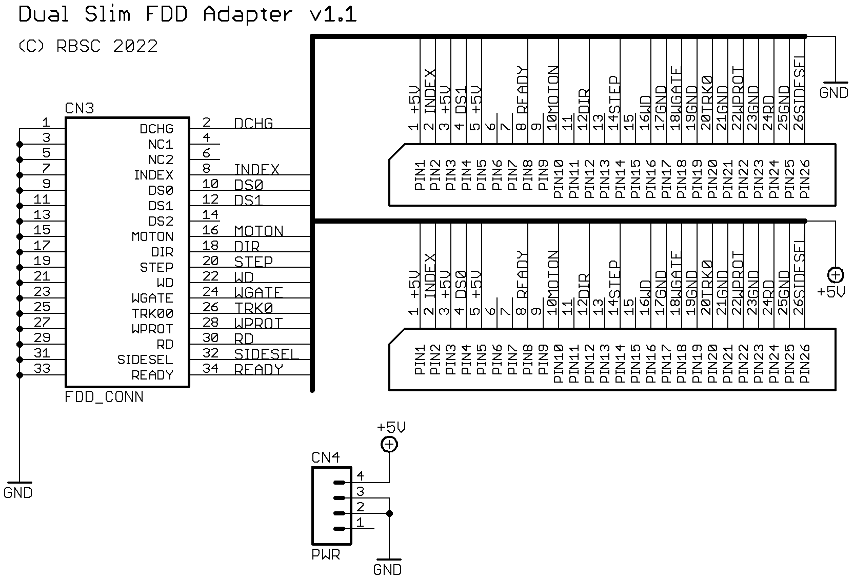
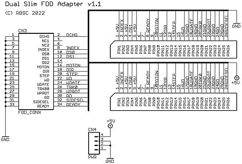
Schaltplan Dual Slim FDD Adapter v1.1
Dual Slim FDD Adapter v1.1 (C) RBSC 2022 CN3 1 DCHG 2 INDEX 3 NC1 4 DS1 5 NC2 6 DS0 7 INDEX 8 READY 9 INDEX 10 MOTON 11 DS0 12 DIR 13 DS1 14 STEP 15 DS2 16 UD 17 MOTON 18 UGATE 18 DIR 19 STEP 20 STEP 20 TK0 21 WD 22 WD 22 APBOT 23 WD 24 WGATE 24 WGATE 25 2KGND 26 SIDESEL
in „Pinbelegung 3,5" Floppy mit FPC26“ · PC Hard- und Software · · Schaltpläne
-
Datei
temp_str.c
((TWCR & (1<<TWSTO))); #if defined(ARDUINO) #if ARDUINO >= 100 //check busy Wire.beginTransmission(DS1307_ID); printIIC(STATUS_REGISTER); Wire.endTransmission(); Wire.requestFrom( ( DS1307_ID ), 1); // request Status Register 1 Byte if ((readIIC() & 0x00ff) & (1<<BSY)) // auf busy pruefen mit 0x00ff
in „RTC DS3231 - Temperatur Daten?“ · Mikrocontroller und Digitale Elektronik ·
-
PDF
MT48LC16M16A2.PDF
AS AH ALL BANKs A10 ROW ROW DISABLE AUTO PRECHARGE SINGLE BANK tAS AH BA0, BA1 BANK BANK BANK BANK tDS tDH DS tDH DS DH tDS DH DINm DINm + 1 DINm + 2 DINm + 3 DQ tRCD t 3 RP WR tRAS tRC DON’T CARE Notes: 1. For this example, BL = 4, and the WRITE burst is followed by a “manual” PRECHARGE. 2. 14ns to 15ns
in „[Verkaufe] 5xSDRAM (4Meg x 16 x 4 Banks) und 5xFLASH (64Meg 8 o. 16 Bit)“ · Markt ·
-
PDF
DS-TWN4-MultiTech-LEGIC-42_DocRev14.pdf
option available on request + 3D construction data (STEP) available on request © 2019 – ELATEC GmbH – DS TWN4 MultiTech LEGIC 42 – DocRev14 – 9/2019 Page 1 of 3 TECHNICAL DATA FREQUENCY 125 kHz/134.2 kHz (LF) / 13.56 MHz (HF) ANTENNA Integrated HOUSING Material: ABS UL94-V0, color: black or white DIMENSIONS
in „Erbitte Hilfe bei RFID Projekt Tierchip von Streunerkatzen auslesen“ · Offtopic ·
-
PDF
datasheet.pdf
On-State Resistance (VGS = 10V, 0.5D[Cont.] 0.011 Ohms Zero Gate Voltage Drain Current (= V , V = 0V) I DS DSS GS 250 A DSS Zero Gate Voltage Drain Current (= 0.8 V , V = 0V, T = 125°C) 1000 DS DSS GS C GSS Gate-Source Leakage Current (GS= ±30V, VDS = 0V) ±100 nA VGS(th) Gate Threshold Voltage DS = VGS, D
-
 Bild
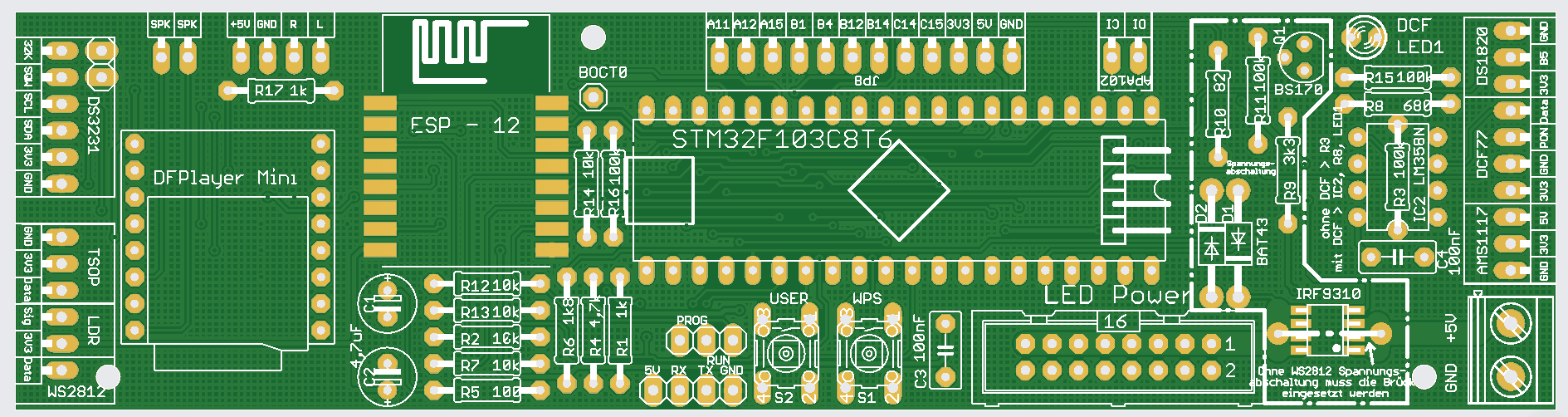
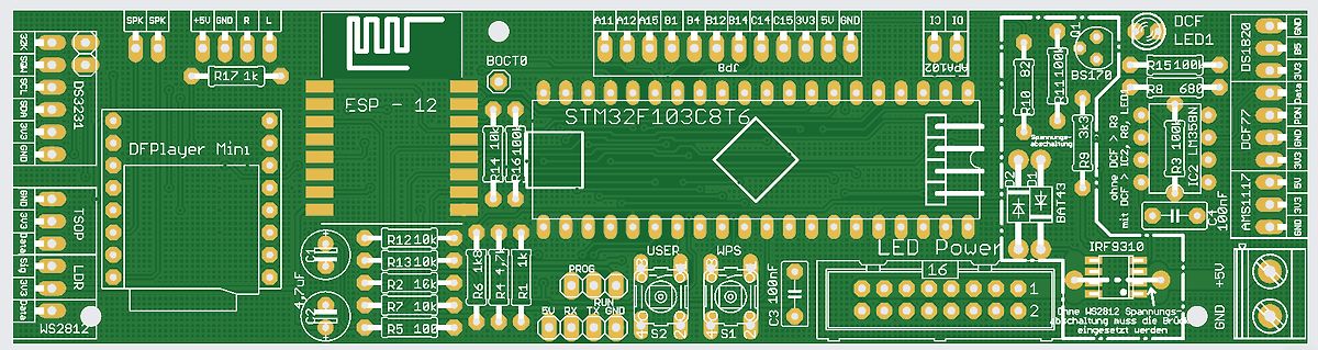
Leiterplatten-Layout eines ESP-12 STM32F103C8T6 Projekts
SPK SPK +5V GND R L BOCT0 R17 1k ESP - 12 STM32F103C8T6 A11 A12 A15 B1 B12 B14 C14 C15 3V5 GND IC IO Q1 DCF LED1 DS1820 R15 100R 28 68 GND PIN 3V5 DS1820 R10 82 BS170 Q2 IC2 LM358 R9 3k R8 LED DCF 100nF R3 100R IC2 R2 10k R14 10k R16 100R R12 10k R13 10k R2 16k R4 4.7uF R7 10k
in „WordClock mit WS2812“ · Projekte & Code · · Layouts
-
PDF
MOSFET-irfiz34v.pdf
Technology D l Ultra Low On-Resistance V DSS = 60V l Dynamic dv/dt Rating l 175°C Operating Temperature R DS(on) = 28m l Fast Switching G l Fully Avalanche Rated I = 20A l Optimized for SMPS Applications S D Description AdvancedHEXFET ® PowerMOSFETsfromInternational Rectifierutilizeadvancedprocessingtechniquestoachieve
in „Frage zur Optokoppler“ · Mikrocontroller und Digitale Elektronik ·
-
PDF
multimec-5-series-switches.pdf
/2B min. 15.24 x 15.24.16min. switch spa15.1 x 15.1 10.1 12.7 x 12min.W15.5 x 15.5 10.54ø9.6 ø10.0 14.3 x 14min. panel cut-out 14.7 x 14.7 1B/1C+1D/1E/1F 1K 15.24 12.7 x 12.7 1KA 15.24 x 15.24.6 15.24 x 15.24x 14.3ø10.0 10.16 14.3 x 14.37 x 14.75.0 x 10.1 14.7 x 14.75 25.7 x 10.5 1A 1D/1E/1FF1C+2A/2B
in „[S] Beleuchtete Navimec Navigationskreistaster für Prototypenherstellung“ · Markt ·
-
PDF
CLIPDecoder_Antoniak.pdf
16V 8 R9 R13 D R16 R6 9 1k5 2M2 1k AGND AGND 100k R10 100k C6 R4 10n CLIP_DIG 100k C4 5 AGND 2n2 7 R14 T1 M1 AGND AGND 6 BC548B VIN 10k 1,5A R2 C1 C2 R15 3 4 U1B 1 R11 R12 12 TL084 1k2 CON1 1k2 10n/100V 2n2 2 14 TEL R1 R3 D2 11 33k 33k 13 22k 33k D1 C5 1N41481N4148 1n AGND U1A R7 TL084 U1C GND GND AGND
in „Kryptischer CLIP-Decoder“ · Mikrocontroller und Digitale Elektronik ·
-
PDF
CLIPDecoder_Antoniak.pdf
16V 8 R9 R13 D R16 R6 9 1k5 2M2 1k AGND AGND 100k R10 100k C6 R4 10n CLIP_DIG 100k C4 5 AGND 2n2 7 R14 T1 M1 AGND AGND 6 BC548B VIN 10k 1,5A R2 C1 C2 R15 3 4 U1B 1 R11 R12 12 TL084 1k2 CON1 1k2 10n/100V 2n2 2 14 TEL R1 R3 D2 11 33k 33k 13 22k 33k D1 C5 1N41481N4148 1n AGND U1A R7 TL084 U1C GND GND AGND
in „Festnetzklingel mit Arduino“ · Mikrocontroller und Digitale Elektronik ·
-
PDF
00954A.pdf
, implicitly or otherwise, under any intellectual Analog-for-the-Digital Age, Application Maestro, dsPICDEM, property rights. dsPICDEM.net, dsPICworks, ECAN, ECONOMONITOR, FanSense, FlexROM, fuzzyLAB, In-Circuit Serial Programming, ICSP, ICEPIC, Migratable Memory, MPASM, MPLIB, MPLINK, MPSIM, PICkit,
in „Kondensatornetzteil: Frage.“ · Mikrocontroller und Digitale Elektronik ·
-
PDF
transformerless_AC_DC.pdf
, implicitly or otherwise, under any intellectual Analog-for-the-Digital Age, Application Maestro, dsPICDEM, property rights. dsPICDEM.net, dsPICworks, ECAN, ECONOMONITOR, FanSense, FlexROM, fuzzyLAB, In-Circuit Serial Programming, ICSP, ICEPIC, Migratable Memory, MPASM, MPLIB, MPLINK, MPSIM, PICkit,
in „230V AC auf 5V DC Bauteile“ · Mikrocontroller und Digitale Elektronik ·
-
PDF
LM386_Low_Voltage_Audio_Power_Amplifier.pdf
Peak-to-Peak Output Voltage vs Supply Voltage (Referred to the Output) Swing vs Supply Voltage vs Frequency DS006976-5 DS006976-13 DS006976-12 Voltage Gain vs Frequency Distortion vs Frequency Distortion vs Output Power DS006976-14 DS006976-15 DS006976-16 Device Dissipation vs Output Device Dissipation vs Output
in „Elektretmikrofon und LM 386N-1 als Verstärker“ · Mikrocontroller und Digitale Elektronik ·
-
PDF
lm386.pdf
Peak-to-Peak Output Voltage vs Supply Voltage (Referred to the Output) Swing vs Supply Voltage vs Frequency DS006976-5 DS006976-13 DS006976-12 Voltage Gain vs Frequency Distortion vs Frequency Distortion vs Output Power DS006976-14 DS006976-15 DS006976-16 Device Dissipation vs Output Device Dissipation vs Output
in „Spannanungsverstärkung“ · Analoge Elektronik und Schaltungstechnik ·
-
PDF
sch_lay.pdf
DS4 DS5 S1B DS8 DS91 2 S2B 0 0 0 0 DS7 0 0 9 9 S S S S P0S1BR8 S S D D P0S2B0R81 2 0 0 0 0 P0S1B03 0 0 0 0 0 0 P0S2B03 0 0 DS1 2 P P P P DS60 0 P0S1B00 R 0 0 P P P P P0S2B00 8 8 0 0 S S P P S S DS00 0 0
in „signal- bzw. funktionsgenerator mit OPs“ · Analoge Elektronik und Schaltungstechnik ·
-
PDF
Si2302.pdf
Si2302DS Vishay Siliconix N-Channel 1.25-W, 2.5-V MOSFET ▯▯▯D▯C▯ ▯▯▯▯▯▯▯ V (V) r (▯) I (A) DS DS(on) D 0.085 @ VGS = 4.5 V 2.8 20 0.115 @ VGS = 2.5 V 2.4 TO-236 (SOT-23) G 1 3 D S 2 Top View Si2302DS (A2)* *Marking
in „Highside-Switch gesucht“ · Analoge Elektronik und Schaltungstechnik ·
-
PDF
70628.pdf
Si2302DS Vishay Siliconix N-Channel 1.25-W, 2.5-V MOSFET ▯▯▯D▯C▯ ▯▯▯▯▯▯▯ V (V) r (▯) I (A) DS DS(on) D 0.085 @ VGS = 4.5 V 2.8 20 0.115 @ VGS = 2.5 V 2.4 TO-236 (SOT-23) G 1 3 D S 2 Top View Si2302DS (A2)* *Marking
in „MOSFET CJ2302 geht kaputt?“ · Analoge Elektronik und Schaltungstechnik ·
-
PDF
AQ_Rly_Dm_lcd_lan_1_wire_18_11_12.pdf
type_s = 0; break; default: Serial.println("Device is not a DS18x20 family device."); return; } ds.reset(); ds.select(addr); ds.write(0x44,1); // start conversion, with parasite power on at the end delay(1000); // maybe 750ms is enough, maybe not // we might do a ds.depower() here, but the reset will take care of it. present = ds.reset(); ds.select(addr); ds.write(0xBE); // Read Scratchpad Serial.print(" Data = "); Serial.print(present,HEX); Serial.print(" "); for
in „Aquariumcontroller: hängt sich auf / stürzt ab / friert ein - Hilfe!“ · Mikrocontroller und Digitale Elektronik ·
-
PDF
A4979-Datasheet.pdf
1.508.853.5000; www.allegromicro.com A4979 Microstepping Programmable Stepper Motor Driver STEP D15=1 and D14=0 L M STRn C A B D E SCK J K SDI X D15 X D14 X D0 X F I G SDO Z D15' D14' D0' Z H Figure 1. Serial Interface Timing Diagram Key Characteristic Key Characteristic A Clock High Time H Data Out Valid Time
in „Schrittmotor-Treiber-IC mit umfangreichen Programmiermöglichkeiten und Diagnose-Funktionen“ · Mikrocontroller und Digitale Elektronik ·
-
PDF
AvrBoard.pdf
Data6) 8 1 e 2 20 2 5 3PD1 mPC36 (Data5) 7 A 2 19 100n 3 4 4PD2 PC25 (Data4) 6 2 2 18 4 3 3 5PD3 PC14 (Data3) 5 D X S 5 A 2 6PD4 PC03 (Data2) 4 B 100n M 100n 5x 2 6 1 7Vcc AGnd2 BAT46 (Data1) 3 m ä 7 CTS 0 8Gnd ARef1 (Data0) 2 n . 8 RTS 9 9Xtal1 AVcc0 220 1 14 100n 2x22p 0Xtal2 PB59 3,6864MHz 1PD5 PB48
-
PDF
AvrBoard.pdf
Data6) 8 1 e 2 20 2 5 3PD1 mPC36 (Data5) 7 1 A 2 19 100n 3 4 4PD2 PC25 (Data4) 6 2 1 2 18 4 2 3 5PD3 PC14 (Data3) 5 D X S 5 A 2 6PD4 PC03 5x (Data2) 4 B 100n M 100n 5 6 1 7Vcc AGnd2 BAT46 (Data1) 3 m ä 7 CTS 0 8Gnd ARef1 (Data0) 2 n . 8 RTS 9 9Xtal1 AVcc0 220 1 14 100n 2x22p 0Xtal2 PB59 3,6864MHz 1PD5 PB48
in „LED flackern“ · Mikrocontroller und Digitale Elektronik ·
-
PDF
TWI_logger_readme.pdf
in 5 Minutenabständen jeweils 6 Temperaturwerte (zuzüglich 4 Byte Zeiteintrag) über die Dauer von 14 Tagen aufzuzeichnen. Bei Bedarf kann der Speicherplatz durch zusätzliche Eeproms erweitert werden. Die Ruhestromaufnahme liegt bei ca. 40uA (bei 4.5 Volt) bzw. ca. 20uA (bei 3.3V). Während der Messung
in „TWI-Datenlogger mit M88, PCF8583, AT24C512 (+ DS18B20) für den Batteriebetrieb“ · Projekte & Code ·
-
PDF
AvrBoard__1_.pdf
Data6) 8 1 e 2 20 2 5 3PD1 mPC36 (Data5) 7 1 A 2 19 100n 3 4 4PD2 PC25 (Data4) 6 2 1 2 18 4 2 3 5PD3 PC14 (Data3) 5 D X S 5 A 2 6PD4 PC03 5x (Data2) 4 B 100n M 100n 5 6 1 7Vcc AGnd2 BAT46 (Data1) 3 m ä 7 CTS 0 8Gnd ARef1 (Data0) 2 n . 8 RTS 9 9Xtal1 AVcc0 220 1 14 100n 2x22p 0Xtal2 PB59 3,6864MHz 1PD5 PB48
in „portpin PD.3 liefert kein signal“ · Mikrocontroller und Digitale Elektronik ·
-
PDF
8020_8021_Users_Manual.pdf
12-3 ResponseHeader(X) 4-21 4-12-4 ResponseMessageTerminator 4-22 4-13 DeviceStatusReporting 4-22 4-14 StatusByteRegister 4-22 4-14-1 ReadingtheStatusByteRegister 4-23 4-14-1-1 ReadingwithaSerialPoll 4-23 4-14-1-2 Readingwiththe*STB? 4-23 4-14-1-3 ClearingtheStatusByteRegister 4-23 4-14-1-4 Service Request
in „Handbuch für Funktionsgenerator Kontron 8021 gesucht“ · Offtopic ·
-
PDF
2210280930_Diodes-Incorporated-AP63300WU-7_C2158012.pdf
1.0V UVLO VINUndervoltage Rising Threshold — — 3.5 3.7 V VIN Undervoltage Hysteresis — — 440 — mV R DS(ON)1 High-Side Power MOSFET On-Resistance (Note 8) — — 75 — mΩ R DS(ON)2 Low-Side Power MOSFET On-Resistance (Note 8) — — 40 — mΩ IPEAK_LIMIT HS Peak Current Limit (Note 8) — 4.1 4.5 4.9 A VALLEY_LIMIT
in „Step-Down-Wandler pfeift sehr laut, was tun?“ · Digitale Signalverarbeitung / DSP / Machine Learning ·
-
PDF
BF245.pdf
V DS = 15 V; GS = 0; f = 200 MHz − 250 − S gos output conductance V DS = 15 V; GS = 0; f = 200 MHz − 40 − S y forward transfer admittance V = 15 V; V = 0; f = 1 kHz 3 − 6.5 mS fs DS GS V DS = 15 V; GS
in „Vorbereitung auf Klausur“ · Analoge Elektronik und Schaltungstechnik ·
-
PDF
EL12864A.pdf
specified about current flowing througSS. Internal oscillation circuit: Rf=47kΩ, cf=20pF Each terminals of DS1, DS2, FS, SHL, and MS is connected to DD and out is no load. *4. This value is specified about current flowing througSS. Each terminals is DS1, DS2, FS, SHL, PCLK2 and CR is connected to VDD,MS is connected
in „LCD Display Powertip PG-12864A“ · Mikrocontroller und Digitale Elektronik ·
-
PDF
gdm12864a.pdf
specified about current flowing throuSS.V Internal oscillation circuit: Rf=47kO, cf=20pF Each terminals of DS1, DS2, FS, SHL, and MS is connected to DD and out is no load. *4. This value is specified about current flowing throuSS.V Each terminals is DS1, DS2, FS, SHL, PCLK2 and CR is connected to VDD,MS is connected
-
PDF
AN_165_Establishing_Synchronous_245_FIFO_Communications_using_a_Morph-IC-II.pdf
Morph-IC-II Version 1.1 Clearance No.: FTDI# 221 Time Description Min Max Units ns T1 RD# inactive to RXF# 1 14 T2 RXF# inactive after RD# cycle 49 ns T3 RD# to DATA 1 14 ns T4 RD# active pulse width 30 ns T5 RD# active after RXF# 0 ns T6 WR# active to TXE# inactive 1 14 ns T7 TXE# active to TXE# after WR# cycle
-
PDF
emmc.pdf
Consumption Table 1: MLC Partition Sequential Performance Typical Values (MB/s) Condition 1 4GB 8GB Write 14 22 Read 160 190 Note: 1. Bus in x8 I/O and HS400 modes. Sequential access of 2MB chunk. Additional performance data, such as sys- tem performance on a specific application board, will be provided in
in „Pin-Swap/Cross IC?“ · Mikrocontroller und Digitale Elektronik ·
-
PDF
soft_clip.pdf
R9 R13 8 R16 D R6 9 1k5 2M2 1k D AGND AGND 100k R10 100k C6 R4 10n CLIP_DIG 100k C4 5 AGND 2n2 7 R14 T1 AGND AGND 6 BC548B M1 VIN 10k 1,5A R2 C1 C2 R15 3 4 U1B 1 R11 R12 12 TL084 1k2 CON1 1k2 10n/100V 2n2 2 14 TEL R1 R3 D2 11 33k 33k 13 22k 33k D1 C5 1N4148 1N4148 1n AGND U1A R7 TL084 U1C GND GND AGND
in „CLIP Schaltplan; Protel->PDF Umwandlung bitte“ · Mikrocontroller und Digitale Elektronik ·
-
PDF
LTC1923.pdf
losses in the application shown on the front diagonalsofthebridge.TheMOSFETsshouldbeselected for their DS(ON), gate charge and maximum V DS, VGS page of the data shee2: Input supply current, MOSFET ratings. A maximum V DS rating of 20V is more than switching losses and IR losses. sufficient for 5V and 12V
in „Peltier und PWM?“ · Analoge Elektronik und Schaltungstechnik ·
-
PDF
MOC3041-M.pdf
MOC3031M 2 MOC3032M 5 SCR MOC3033M SCR 180 Ω 3 4 R2 D2 LOAD Figure 14. Inverse-Parallel SCR Driver Circuit (MOC3031M, MOC3032M, MOC3033M) Suggested method of firing two, back-to-back SCR’s with a Fairchild triac driver. Diodes can be 1N4001; resistors, R1 and R2, are optional
in „Triac schaltet nicht ab“ · Mikrocontroller und Digitale Elektronik ·
-
PDF
NVMFS4C03N.pdf
Power, Single N-Channel, Logic Level, SO-8FL 30 V, 1.7 mW, 159 A www.onsemi.com Features V (BR)DSS R DS(on)AX D MAX • Small Footprint (5x6 mm) for Compact Design • Low R DS(on)to Minimize Conduction Losses 1.7 mW @ 10 V 30 V 159 A • Low Q Gnd Capacitance to Minimize Driver Losses 2.4 mW @ 4.5 V • NVMFS4C03NWF
in „Wahl des SynchrongleichrichterMOSFETs für Buck Converter“ · Analoge Elektronik und Schaltungstechnik ·
-
PDF
MTP12P10_D-.pdf
onsemi.com 2 MTP12P10 TYPICAL ELECTRICAL CHARACTERISTICS D 20 I 1.2 VGS = −20 V 10 V A 18 M V = V ) O DS GS P 16 TJ= 25°C ( 1.1 D = 1 mA M 8 V E ( 14 A N L R 12 V 1 R 10 7 V L C O I 8 S 0.9 R 6 V R , 6 T ID E − 4 5 V A 0.8 , 2 t 0 S 0 1 2 3 4 5 6 7 8 9 10 VG −50 −25 0 25 50 75 100 125 150 −V DSDRAIN−TO−
-
PDF
DS_SJDP120R085_rev1.3.pdf
Carbide PRELIMINARY SJDP120R085 Normally-On Trench Silicon Carbide Power JFET Product Summary BV 1200 V DS R DS(ON)max 0.085 Ω Features: ETS,typ TBD µJ - Positive Temperature Coefficient for Ease of Paralleling - Extremely Fast Switching with No "Tail" Current at 150 °C - 150 °C Maximum Operating Temperature
in „Siliziumkarbid-JFETS“ · Analoge Elektronik und Schaltungstechnik ·
-
Datei
xFB_RC5_64.c
else lw("-"); step=2; lg(2,8);lw("^"); break; //----------------- neu case(fb_green)://Einstellmenü ds1307 cbi(bool1,schalter_FB_verbose); #if use_glcd lcd_ClearZeilen_Y(0,35,(GOLD)); #else lcd_clear(); #endif ds1307menu=1; lg(1,1);sub_lcd_wdy(WDY); lcd_int2(DAY);lw(".");lcd_int2(MON);lw(".");lcd_int2
in „Menuerstellung GLCD in C“ · Mikrocontroller und Digitale Elektronik ·
-
PDF
BF245abc.pdf
MIN. TYP. MAX. UNIT VDS drain-source voltage − − ±30 V VGSoff gate-source cut-off voltage D = 10 nA; DS = 15 V −0.25 − −8 V VGSO gate-source voltage open drain − − −30 V I drain current V = 15 V; V = 0 DSS DS GS BF245A 2 − 6.5 mA BF245B 6 − 15 mA BF245C 12 − 25 mA Ptot total power dissipation Tamb= 75
in „Welche Steilheit hat ein BF245C?“ · Analoge Elektronik und Schaltungstechnik ·
-
PDF
LM2991.pdf
Typical Performance Characteristics 2 M L Dropout Voltage Normalized Output Voltage Output Voltage DS011260-13 DS011260-14 DS011260-15 Output Noise Voltage Quiescent Current Maximum Output Current DS011260-16 DS011260-17 DS011260-18 Line Transient Response Load Transient Response Maximum Output Current DS011260-19 DS011260-20 DS011260-21 Ripple Rejection Output Impedance ON /OFF Control Voltage DS011260-22 DS011260-23 DS011260-24 www.national.com 4 L M Typical Performance Characteristics (Continued) 9
in „Negative Low Dropout Adjustable Regulator gesucht“ · Mikrocontroller und Digitale Elektronik ·
-
Datei
bootloaderV25.a51
DBIT 1 ; 1 if it is a CH551 or CH553 bReqError: DBIT 1 ; 1 on request Errors dseg at 0x21 wValueLo: DS 1 ; 0x21 TimeOut: DS 2 ; new in V2.5 BootKey: DS 8 ; Marker0: DS 1 ; rlen: DS 1 ; reqlen: DS 1 ; cmdbuffer: DS 64 ; DS 2 ; unused bRequest: DS 1 ; SnSum: DS 1 ; DescAddr: DS 2 ; CAddr: DS 2 ; Marker1: DS 1 STACK: xseg at 0 EP0_BUFFER: DS 8 ; 0x0000 the control endpoint DS 4 ; spare EP2_OUT_BUFFER: DS 64 ; 0x000C bulk out EP2_IN_BUFFER: DS 64 ; 0x004C bulk in cseg at StartAddress ; bootloader start ljmp
in „uC für 0,20€ CH552 / CH554 von WCH Billig Micro mit USB Funktion, Chip vorstellung“ · Mikrocontroller und Digitale Elektronik ·
-
PDF
AL5802-DIO.pdf
© Diodes Incorporated Document number: DS35516 Rev. 9 - 2 AL5802 Application Information T C The AL5802 has been designed for driving low current LEDs with typical U LED current of 20mA to 100mA. It provides a cost effective way for D driving
in „Dimensionierung von LED-Dimm-Schaltung“ · Analoge Elektronik und Schaltungstechnik ·
-
PDF
infineon-bsb056n10nn3-g-datasheet-en.pdf
BSB056N10NN3 G Diagram 9: Drain-source on-state resistance Diagram 10: Typ. gate threshold voltage 14 4.0 3.5 12 3.0 10 1000 µA 2.5 ] 100 µA 8 ] m 98 % [ ) t 2.0 ( S D 6 typ G R V 1.5 4 1.0 2 0.5 0 0.0 -60 -20 20 60 100 140 180 -60 -20 20 60 100 140 180 T j°C] Tj[°C] R DS(on)f(Tj; D =30 A; VGS10 V VGS
in „Bauteilsuche Mosfet“ · Analoge Elektronik und Schaltungstechnik ·
-
PDF
fronius_transpocket_1400mw_sm_de.pdf
- Tightenthescrewonthebaseplate(Fig.11) 1)Mustberetrofittedifnotalreadyinstalle2)OnlyonPUU14/PFU14-V1.0C 3)NotonPUU14/PFU14-V1.0C 10 Fig.1 Fig.2 Fig.8 Fig.9 Fig.3 Fig.4 Fig.10 Fig.11 Fig.5 S L G N E Fig.12 Fig.6 Fig.13 Fig.7 Fig.14 Fig.15 11 ADJUSTING THE PFU14 PROCEDUREOFMANUALWELDING CONTROLOFTIG-MODE
in „Fronius Schweißinverter TP 1400 Leistungsteil defekt“ · Analoge Elektronik und Schaltungstechnik ·
-
PDF
datasheet.pdf
x 17mm MC9328MX21DVG 289-lead MAPBGA Lead 0.65mm, 14mm x 14mm -30°C–70 °C MC9328MX21DVK 289-lead MAPBGA Lead-free -30°C–70 °C 0.65mm, 14mm x 14mm MC9328MX21DVH 289-lead MAPBGA Lead -30°C–70 °C 0.8mm, 17mm x 17mm MC9328MX21DVM 289-lead MAPBGA Lead-free
in „PHILIPS VP5500 VoIP Telefon bei Pollin“ · Mikrocontroller und Digitale Elektronik ·