-
Thread
LoRa-Parameter
receiving node receiving node receiving node own high 8bit own low 8bit own # high 8bit address low 8bit address frequency address address
fixed-point transmission, the module will identify the first three bytes of serial port data as: address high + address low + channel, and use them as wireless transmission targets." Der Code sender aber offenbar: - address high - address low - frequency - sender address high - sender address low
-
 Bild
Bild
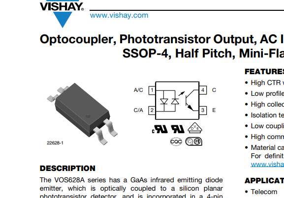
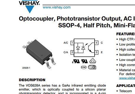
Datenblatt Ausschnitt Vishay Optokoppler VOS628A
Optocoupler, Phototransistor Output, AC I SSOP-4, Half Pitch, Mini-Fla 22628-1 A/C 1 4 C C/A 2 3 E FEATURES High CTR Low profile High collect Isolation te Low coupl High comm Material ca For definit www.vishay DESCRIPTION The VOS628A series has a GaAs infrared emitting diode emitter, which is optically coupled
-
Thread
Optokoppler ohne externen Pull up nur Bias
Unabhängig davon, ob der Optokoppler aktiviert ist oder nicht, liefert der Eingang des SBC s immer ein High. Könnte es sein, dass der interne Pull-up-Widerstand zu groß ist und der Transistor den Pegel nicht zuverlässig auf Low ziehen kann? Sollte ich stattdessen besser einen externen Pull-up mit niedrigerem
davon, ob der > Optokoppler aktiviert ist oder nicht, liefert der Eingang des SBC s > immer ein High. > > Könnte es sein, dass der interne Pull-up-Widerstand zu groß ist und der > Transistor den Pegel nicht zuverlässig auf Low ziehen kann? Sollte ich > stattdessen besser einen externen Pull-up
-
Thread
Charlieplexing mit erhöhter Leistung (Strom/Spannung)
Theoretisch könnte man LowSide Treiber mit Push-Pull Enstufe benutzen wie den IR4426-IR4428. Der IR4426 hat je zwei Treiber, so das 2 dieser Treiberbausteine reichen sollten. Und Strom können sie liefern.
alle leuchten, ausserdem kann es ja für bestimmte Squenzen notwenig sein, das eine Leitung immer High ist. Das wäre nach meinem Verständnis dann DC, eigntlich fängt für den high Side Treiber DC an, wenn die Zeit die das Bootstrap C überbrückt abläuft. Kann je sein, das die 12 LED die Stunden einer
-
Thread
mikrofon an pc
Lautsprechers. Die Lichtschranke würde ich so anschließen, dass die den Reset-Eingang des NE555 auf Low zieht. Ein Pull-Up Widerstand sorgt dann für den HIGH Pegel am Reset Eingang.
-
Thread
Problem mit Relaismodul an Wemos D1 Mini (ESP 8266)
aufgefallen, dass sich das Relais nicht wie von mir erhofft schalten lässt. Es ist immer an; Unabhängig von LOW oder HIGH am ESP Ausgang. Ich verwende ein "JQC3F-05VDC-C" Relais. Ein Bild davon ist im Schaltplan. Ich habe zum Test einen einfachen Blink Sketch auf den ESP geflashed und gemerkt, dass selbst
define RELAIS_PIN D6 void setup() { pinMode(RELAIS_PIN, OUTPUT); digitalWrite(RELAIS_PIN, HIGH); } void loop() { digitalWrite(RELAIS_PIN, LOW); delay(3000); digitalWrite(RELAIS_PIN, HIGH); delay(3000); }[/c]
-
 Bild
Bild
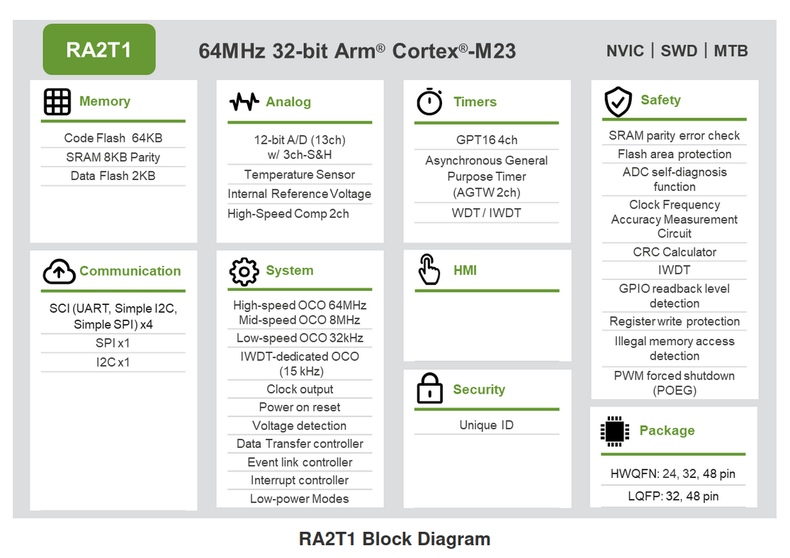
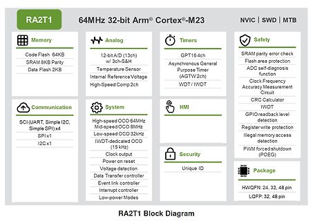
Blockschaltbild RA2T1 Mikrocontroller
Data Flash 2KB Analog 12-bit A/D (13ch) w/ 3ch-S&H Temperature Sensor Internal Reference Voltage High-Speed Comp 2ch Timers GPT 16ch Asynchronous General Purpose Timer (AGTW 2ch) WDT / IWDT Safety SRAM parity error check Flash area protection ADC self-diagnosis function Clock Frequency Accuracy Measurement
-
Thread
Anfänger Lötstation zum Steuergeräte reparieren
Aliexpress besorgt, also ein Bausatz, weil ich das auch für KFZ sehr cool fand, klar ich kann kein CAN high und Low vergleichen, gleichzeitig, aber sorgt für besseres Verständnis. Eine gute Zange habe ich, eine Lampe mit Lupe hat mein Vater. Pinzetten hab ich bestellt und Lötzinn hätte ich von meinem
Aliexpress besorgt, also ein Bausatz, > weil ich das auch für KFZ sehr cool fand, klar ich kann kein CAN high > und Low vergleichen, gleichzeitig, aber sorgt für besseres Verständnis. Es ist eine nette Spielerei und du kannst Löten und Messen üben. Gehe nicht davon aus, dass es wahnsinnig toll sein wird
-
Thread
ATtiny1614 mit externen 32.768khz Quartz
sich auf die Fuses: Ich möchte den externen Quarz als CPU-Takt betreiben. Welcher CKSEL-Fuse-Wert (Low-Fuse) und welche STARTUP-Option (High-Fuse) sind dafür nötig? Ich programmiere mit avrdude über UPDI – Ich habe das Gefühl ich habe hier die falschen Werte: -U lfuse:w:…:m -U hfuse:w:…:m -U efuse
Paul schrieb im Beitrag #7903081: > Welcher CKSEL-Fuse-Wert (Low-Fuse) und welche STARTUP-Option (High-Fuse) > sind dafür nötig? Da läuft bei diesen Chips sehr viel über Register, nicht über Fuses. z.B.: 23.4 RTC Functional Description
-
Thread
PWM mit PIC12F1501
Bin keine Experte, aber: - versuche mal High and Low zu vertauschen. Bei manchen PICs waren Timers so, dass man die reihenfolge richtig machen musste. Wobei das war eher bei lesen. Meine ich. - Versuche nur den High zu schreiben. Lass den low
angewöhnt, die in ASM zu benutzen. Na wenn Du Spaß daran hast, viel Schreibarbeit für den ganzen Low-Level Schrunz auf Dich zu nehmen. Auch bei 8-Bittern erhöht C drastisch die Lesbarkeit und verringert Fehlerquellen, weil man sich besser auf die eigentlichen Abläufe fokussieren kann.
-
Thread
Projektverzug und Bugdichte in der FPGA-Entwicklung
Kann aber sein, das mit der Migration zu "Chinesischen" und damit zu FPGA's die näher am klassischen Low-Cost Design des Spartan-3 wieder die Implementierung auf geringe Ressourcenbedarf und kurze Signalpfade optimiert. > Oder wenn der Layouter 8 Hispeed-Lanes swappen muss, weil der Softwerker > keine
erfordert sinnvollerweise einiges an Wissen um Layout-Themen beim FPGA-Designer - gerade im Bezug auf high speed busse, Verdrahtungsanforderungen, Lagenaufbau des PCBs, sowie die Wirkung von Steckern und Vias auf die Signale. Wenn man den Layouter damit alleine lässt, kriegt man gfs Gemüse zurück! Was
-
Thread
Frequenzanzeige und LM7001 mit ATTiny2313 macht mir Probleme..
[avrasm] ldi zl, low(digit_table) ldi zh, high(digit_table) [/avrasm] Muss an den drei Stellen nicht jeweils *2 stehen?
Hi >ShowDigit: > lsl temp > ldi ZL, low(SEG_TABLE * 2) > ldi ZH, high(SEG_TABLE * 2) > add ZL, temp > adc ZH, r1 << > lpm temp, Z r1 ist in dem Programm kein Wert zugewiesen- MfG Spess
-
Thread
Neue Bauteile: DB9-Stecker mit Push-Pull, m5Stack-Module, Kelvinklemmen uvam
Funkmodul aus, dessen Datenblatt die folgenden Spezifikationen anführt: [c] ype 2FY is a small and high performance module based on Infineon CYW55513 combo chipset which supports Wi- Fi® 802.11a/b/g/n/ac/ax + Bluetooth® 5.4 BR/EDR/LE up to 143Mbps PHY data rate on Wifi and 3Mbps PHY data rate on Bluetooth
denkt instinktiv an AWGs und ähnliche metrologische Geräte. Weniger bekannt ist, dass es auch im High End-Audiobereich Bedarf an spezialisierten DACs gibt. Für sein neuestes Angebot – das Datenblatt verspricht einen “32bit Premium DAC mit zwei Kanälen” – vermeldet Asahi neben der Verfügbarkeit verschiedener
-
 Bild
Bild
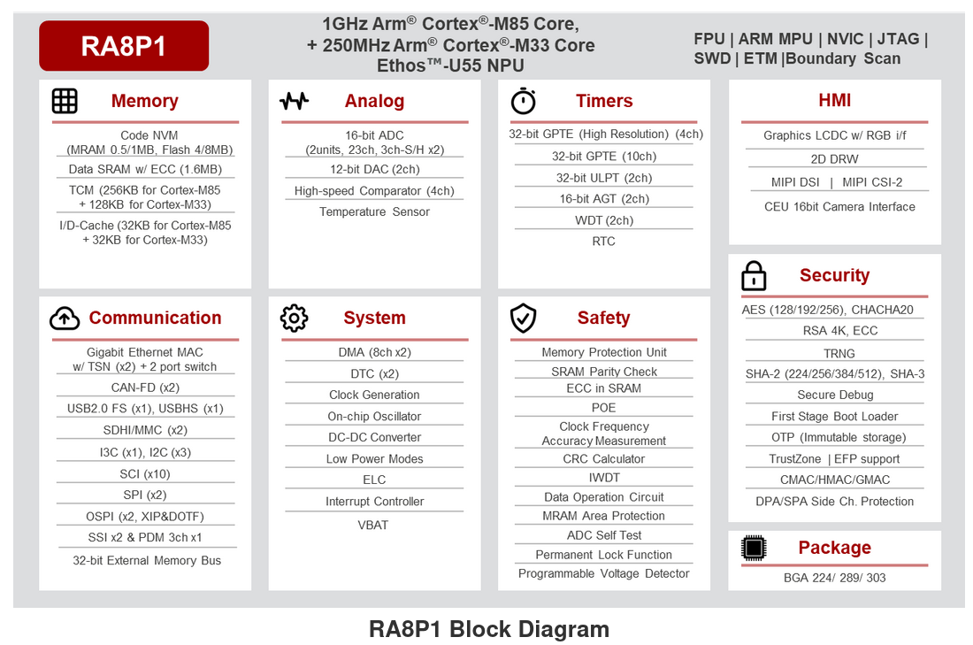
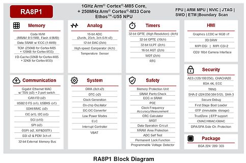
Blockschaltbild des RA8P1 Mikrocontrollers
for Cortex-M85 + 32KB for Cortex-M33) Analog 16-bit ADC (2units, 2ch (3ch-S/H x2) 12-bit DAC (2ch) High-speed Comparator (4ch) Temperature Sensor Timers 32-bit GPTE (High Resolution) (4ch) 32-bit GPIE (10ch) 32-bit ULPT (2ch) 16-bit AGT (2ch) WDT (2ch) RTC HMI Graphics LCD w/ RGB i/f 2D DRW MIPI CSI |
-
Thread
Fehlerhafte RO Idle Polarität ESP8266 <- MAX485
ESP8266 mit dem MAX-Modul verbunden werden erhalte ich eine falsche Polarität, zumindest aber einen Low-Pegel im Idle Zustand. Folgendes Scope-Sweep zeigt das Problem: [MAX485_not_working.png] Bei anderer Kombination ist die Kommunikation erfolgreich: [MAX485_working.png] Läuft! Also dachte ich mir
ESP8266 mit dem MAX-Modul verbunden werden > erhalte ich eine falsche Polarität, zumindest aber einen Low-Pegel im > Idle Zustand. Dann steuerst du das MAX485-Modul falsch an.
-
Thread
Raspberry Pi-Funkmodul, CircuitPython-Update, MicroAI uvam
offers room-filling LiFi coverage of over 80 Sq. Metres and provides Gbps capacity, making it the highest-performing LiFi system available on the market for government and defence which complies with IEEE 802.11bb standard. All pureLiFi systems are based on IEEE 802.11 protocols, making them the simplest
components in power-by-light systems. However, their use in long-distance applications has been hindered by low efficiencies and output voltages within the optical fiber transmission window of 1.3–1.6 μm laser wavelengths. Here, we improve and simplify the design and characterization processes for photonic power
-
Thread
Küchenmaschine Elektronikfehler
sein Gate auf -5V gehenüber MT1, damit er nur Quadranten 2 und 3 und nicht 1 und 4 zünden muss. Also high=aus, low=zünden. https://apollo.neocities.org/electromotiveforces/triac
-
Thread
Falsche Farben bei LVGL - Endianess
falsche Farben dargestellt. Die Ursache ist, dass LVGL die 16-bit Pixelwerte im Little-Endian-Format mit low-Byte voran im Framebuffer ablegt, das Display sie aber als Big-Endian haben will, also high-Byte zuerst. Dies ist in der Doku von LVGL auch beschrieben: "You may set LV_COLOR_16_SWAP in lv_conf.h
colors via a byte-oriented interface like SPI. As 16-bit numbers are stored in little-endian format (lower byte at the lower address), the interface will send the lower byte first. However, displays usually need the higher byte first. A mismatch in the byte order will result in highly distorted colors."
-
Thread
LoRA-Cloud vor Abschaltung, STM32-WLAN-Modul, neue Weltraum-Bauteile uvam
soeben seinen langjährigen Partner aufgekauft hat: [c] Nordic Semiconductor, a global leader in low-power wireless connectivity solutions, today announces the acquisition of its long-term partner, Memfault Inc., the market-leading cloud platform provider for large-scale deployments of connected products
-28 is available with 5V triple outputs that are optimal for use with point-of-load converters and low-dropout linear regulators to power FPGAs and microprocessors (MPUs). The small-form-factor SA15-28 weighs 60 grams and is approximately 1.68 cu inch to optimize the Size, Weight and Power (SWaP) of
-
Thread
Komischer Fehler im Amiga 500
mal an U3 (Paula) gemessen. Pin 18 (_INT6 von U8, CIA-B) geht nach dem Cracker Intro dauerhaft auf LOW. Die beiden anderen Pin 17 und 16 bleiben HIGH. In der fraglichen Sequenz mit der Störung pulst _INT3 von U2 (Agnus) mit ca. 2kHz. > BTW: der Referent "schwärmte" von einem speziellen Diagnose ROM
beim Agnus 50 ns Set und Hold für den Reset drinstehen. Bei CMOS will man eigentlich 4.4V für ein High am Ausgang, da scheint der Reset schon vorher auf die Bremse zu steigen. Aber da das obere Limit für den Low-Pegel von 0.5V flott erreicht ist, passt es wohl bestens. Also zur Analyse musste man
-
Thread
40khz mit ESP32 erfassen
Was denn nun, HIGH Pegel oder analoges Signal? Ersteres solltest Du mit pulseIn() erfassen können.
differential ? 0 : 1) << 7) | (channel << 4); spi_dev->beginTransaction(); //digitalWrite(_cs, LOW); directWriteLow(_cs); spi_dev->transfer(buffer, 3); //digitalWrite(_cs, HIGH); directWriteHigh(_cs); spi_dev->endTransaction(); return (((uint16_t)(buffer[1] & 0x07)) << 8) | buffer
-
Artikel
MOSFET-Übersicht
Treiber-Dimensionierung Treiber-Typ: Low = Low-Side-Treiber (ohne Potenzialversatzstufe) High = High-Side-Treiber ( mit Potenzialversatzstufe) High + Low = beide Treiber mit getrennten Logikeingängen Halbbrücke = beide Treiber mit gemeinsamem
peak 4.5-18V 3.3V - VDD+0.3V SOT-23-5 TME 0,76 € MAX626 2 x Low, inverting ? ? 4,5-18 V DIL8/SO8 Rei 3,40 € NCP5106 High + Low 250/500mA 600V 2,3-20V DIL8/SO8 Far 2,37 € NCP5304 High + Low 250/500mA 600V 2,3-20V DIL8/SO8 Far 2,02 € FAN7380 Halbbrücke 90/180mA 600V
-
Thread
Verständnis von Pull-Up- und Pull-Down-Widerständen bei Taster-Eingängen mit STM32
bei Tastern. Ich habe gelesen, dass es davon abhängt, ob der Logikpegel beim Loslassen des Tasters HIGH oder LOW sein soll. Allerdings habe ich sowohl Beispiele mit internen Pull-Ups als auch mit externen Pull-Downs gesehen. Könnte mir bitte jemand erklären wann sollte man einen Pull-Up anstelle eines
Ruhezustand heraus, entweder nach HIGH oder nach LOW. In diesem geschalteten Zustand ist der Widerstand sowohl mit HIGH als auch mit LOW verbunden, es fließt also ein Strom. Der Widerstand ist möglichst groß (hochohmig) zu wählen, so
-
 Bild
Bild
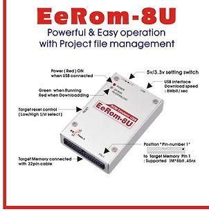
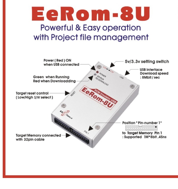
EeRom-8U ROM Emulator mit Beschriftungen
management Power (Red) ON when USB connected Green when Running Red when Downloading Target reset control (Low/High S/W select) RESET ROM Emulator USB EeRom-8U USB Interface Download speed: 8Mbit/sec 5v/3.3v setting switch Position * Pin-number 1* to Target Memory Pin 1 Supported 1M*8bit, 45ns Target Memory