-
PDF
NUVOTON_M058_M0516.pdf
AD10 7 6 AA10 AD3 8 D2 Q2 9 AA3 AD11 8 D2 Q2 9 AA11 AD4 13 D3 Q3 12 AA4 AD12 13 D3 Q3 12 AA12 AD5 14 D4 Q4 15 AA5 AD13 14 D4 Q4 15 AA13 S S AD6 17 D5 Q5 16 AA6 AD14 17 D5 Q5 16 AA14 S S AD7 18 D6 Q6 19 AA7 AD15 18 D6 Q6 19 AA15 A D Reset Circuit D7 Q7 D7 Q7 ALE 11 ALE 11 1 LE D 1 LE D CB3 CB4 OE G OE
in „ARM Cortex M0 NUVOTON M058ZBN auslesen / flashen“ · Mikrocontroller und Digitale Elektronik ·
-
PDF
176141-da-01-en-DS_1621_1621S.pdf
a START condition. TX RX <address,0> Bus Master sends DS1621 address; R/W = 0. RX TX ACK DS1621 generates acknowledge bit. TX RX ACh Bus Master sends Access Config command protocol. RX TX ACK DS1621 generates acknowledge bit. TX RX 02h Bus Master sets up DS1621
in „Temperatursensor DS1621 über I²C ansteuern“ · Mikrocontroller und Digitale Elektronik ·
-
PDF
top222y.pdf
generate a temperature-compensated current source voltage, V with a threshold voltage. High drain DS(ON) sourcewhichistrimmedtoaccuratelysettheoscillatorfrequency currentcausesV DS(ON)toexceedthethresholdvoltageandturns C 4 12/97 TOP221-227 VIN VIN DRAIN 0 V OUT 0 I OUT 0 1 2 8 1 2 8 1 • • • • • • V
in „Suche Ersatz für TOP222Y“ · Mikrocontroller und Digitale Elektronik ·
-
PDF
NCO8703.pdf
190 ≈ 220 pF. The optimum load resistance for class-AB can be determined with formula: R L (0.85 × V DS ) /(2 × O ) For V DS = 50 V and P O 150 W we get R = 6L . To keep the transformer simple a transformation ratio of 4 or 9 is preferable. A ratio of 4 gives a load impedance of 50/4 = 12.5 → 6.25 for
in „Stackpole Ferrit Kerne für RF Verstärker“ · HF, Funk und Felder ·
-
PDF
GL10N10B4S.pdf
Description: VDSS 100 V The GL10N10B4S uses advanced trench technology and ID 10 A design to provide excellDS(ON)ith low gate charge. It PD 40 W R 110 mΩ can be used in a wide variety of applications. The packageDS(ON)type form is TO-252, which accords with the RoHS standard. TO-252 Features: RDS(ON)140mΩ
in „LED-Strip flackert, trotz 1.5kHz dimmfrequenz.“ · Mikrocontroller und Digitale Elektronik ·
-
PDF
2108182030_GL-GL10N10B4S_C2886410.pdf
Description: VDSS 100 V The GL10N10B4S uses advanced trench technology and ID 10 A design to provide excellDS(ON)ith low gate charge. It PD 40 W R 110 mΩ can be used in a wide variety of applications. The packageDS(ON)type form is TO-252, which accords with the RoHS standard. TO-252 Features: RDS(ON)140mΩ
in „Betrieb von MOSFETS bei maximalstrom?“ · Analoge Elektronik und Schaltungstechnik ·
-
PDF
IRLML6401.pdf
WIDTH Tj = 150°C Tj = 25°C 0.01 0.01 0.1 1 10 100 0.1 1 10 100 -V , Drain-to-Source Voltage (V) -V DS , Drain-to-Source Voltage (V) DS Fig 1. Typical Output Characteristics Fig 2. Typical Output Characteristics 2.0 100.0 ID= -4.3A c a Α TJ= 25°C i ( s n R 1.5 r T J 150°C n u 10.0 O d C e e r r zl u o
in „3,3 V schalten mit möglichgst geringem Spannungsabfall“ · Analoge Elektronik und Schaltungstechnik ·
-
PDF
LPW5208.pdf
2.5 6 V I Output Current Limited RL=2Ω 1200 1500 1700 mA LIMIT OUT Output Continue Current 1200 mA R DS(ON) Output N-MOSFET R DS(ON) 160 mΩ I Quiescent Current V =3V 16 28 µA Q IN ISHDN Shutdown Current V ENND 1 µA VEN(L) Enable Threshold Low 0.4 V VEN(H) Enable Threshold High 1.4 V IEN Input High Current
in „sot23(?)-5, 4woel, Datenblatt wg. evtl. Übertemperaturdefekt“ · Analoge Elektronik und Schaltungstechnik ·
-
Datei
PLC-LOX.ino
digital inputs 17-24 8 analog input 1 0-256 9 analog input 2 0-256 10 service - reset (bit 0) 11 1st DS2438 Temp (value multiplied by 100) 12 1st DS2438 Vad (value multiplied by 100) 13 1st DS2438 Vsens (value multiplied by 100) - 39 DS2438 values (up to 10 sensors) 40-50 DS18B20 Temperature (up to 10
in „1 Wire auf 2 GPIO pins“ · Mikrocontroller und Digitale Elektronik ·
-
PDF
Micrel.pdf
2-14: MIC2915x Load Transient. FIGURE 2-17: MIC2915x Line Transient. FIGURE 2-18: MIC2915x Line Transient. FIGURE 2-15: MIC2915x Load Transient. 2016-2019 Microchip Technology Inc. DS20005685B-page 11 MIC2915X
-
PDF
STD60N55F3.pdf
= 10V, I = 32A DS(on) resistance GS D 6.5 8.5 mΩ Table 4. Dynamic Symbol Parameter Test conditions Min Typ. Max. Unit (1) Forward transconductance V =25V, I =32A 50 S gfs DS D Ciss Input capacitance 2200 pF C Output capacitance
in „Frage zu MOSFET STF60N55F3“ · Mikrocontroller und Digitale Elektronik ·
-
PDF
LTC_201.pdf
110 65 125 Ω D TMAX 160 160 Ω ∆R ONvs VS 20 20 % ∆R ONvs Temperature 0.5 0.5 %/°C R ONMatch VS= 0V, DS= 1mA 5 5 % Off Input LeakagS I (OFF) VD= ±14V, VS= ±14V 0.01 ±1 0.01 ±5 nA Switch Off ● ±100 ±100 nA 201a23fb 2 LTC201A/LTC202/LTC203 U DIGITAL A D DC ELECTRICAL CHARACTERISTICS The● denotes the specifications
in „Meßverstärker für 1/f-Rauschen 0.1 - 10 Hz“ · Analoge Elektronik und Schaltungstechnik ·
-
Datei
DS18S20.c
malfunction. */ /* */ /****************************************************************************/ void DS18_InitPort(void) /* t/us = 4.441 + 6.510 + t(CALL:14T) + t(RET:10T) */ /* t = (4.441 + 6.510 + 4.883) us = 15.834us */ { /* The data line must be held high to provide power to the DS18B20 */ DS18_SetPortHigh
in „DS18S20 mit Infineon Mikrocontroller“ · Mikrocontroller und Digitale Elektronik ·
-
Datei
Send_to_R_DS18B20.ino
Chantrell http://nathan.chantrell.net // Updated by Martin Harizanov (harizanov.com) to work with DS18B20 // To use with DS18B20 instead of TMP36, a 4K7 resistor is needed between the Digital 9 and Digital 10 of the ATTiny (Vdd and DQ) // To get this to compile follow carefully the discussion here:
in „DS18B20 Sensoren zeigen immer wieder -127°C an“ · Mikrocontroller und Digitale Elektronik ·
-
PDF
MOSFET_TK6A60W_Toshiba_LIN.pdf
specified) Characteristics Symbol Test Condition Min Typ. Max Unit Gate leakage current IGSS V GS= ±30 V, DS = 0 V ±1 µA Drain cut-off current IDSS V DS= 600 V, GS = 0 V 10 Drain-source breakdown voltage V I = 10 mA, V = 0 V 600 V (BR)DSS D GS Gate threshold voltage Vth V DS= 10 V,DI = 0.31 mA 2.7
in „Push/Pull in spannungsgeregelter Stromquelle / Frage zur Auslegung“ · Analoge Elektronik und Schaltungstechnik ·
-
PDF
tk18a60v_en_datasheet_110131.pdf
V, f = 1 MHz 1600 pF iss DS GS Reverse transfer capacitance Crss 5 Output capacitance Coss 40 Effective output capacitance C o(er) VDS = 0 to 400 VGSV= 0 V 64 Gate resistance r V = OPEN, f = 1 MHz 10 Ω g DS Switching
in „Mosfet defekt - kann der Ersatztyp verwendet werden?“ · Analoge Elektronik und Schaltungstechnik ·
-
Datei
Clockplot_ino.ino
right servos // - added code to support DS1307, DS1337 and DS3231 real time clock chips // - see http://www.pjrc.com/teensy/td_libs_DS1307RTC.html for how to hook up the real time clock // delete or mark the next line as comment if you don't
in „Plotclock zusammenbauen und programmieren“ · Mikrocontroller und Digitale Elektronik ·
-
Datei
plotclock.c
right servos // - added code to support DS1307, DS1337 and DS3231 real time clock chips // - see http://www.pjrc.com/teensy/td_libs_DS1307RTC.html for how to hook up the real time clock // delete or mark the next line as comment if you don't
in „Plotclock zusammenbauen und programmieren“ · Mikrocontroller und Digitale Elektronik ·
-
PDF
A100_IRF7413_IR.pdf
r D D , ,D ID I 20µs PULSE WIDTH▯ 20µs PULSE WIDTH▯ 1 TJ= 25°C A 1 TJ= 150°C A 0.1 1 10 0.1 1 10 V DS , Drain-to-Source Voltage (V) V DS , Drain-to-Source Voltage (V) Fig 1. Typical Output Characteristics Fig 2. Typical Output Characteristics 100 2.0 e ▯ID = 7.3A c ) t ( i t e e R 1.5 r TJ= 150°C n u
in „MOSFET - Verständnisfrage“ · Analoge Elektronik und Schaltungstechnik ·
-
PDF
CP2104-EK.pdf
interface J1 UART signal access connector J2, J3 GPIO access connector J4 Power connector DS0–DS3 Green GPIO LEDs DS4 Red SUSPEND indicator LED _________ SUSPEND LED J2 DS4 DS3 DS2 P1 P2 RS232 Transceiver CP2104 Pin 1 J3 DS1 Pin 2 J1 J4 DS0 Figure 3. CP2104 Evaluation Board with Default Shorting
in „[V] kleines Eval Kit Silabs CP2104-EK ( USB- RS232)“ · Markt ·
-
PDF
564932.pdf
–30 — — V ID= –10 mA, V GS = 0 voltage Gate to source breakdown V(BR)GSS ±20 — — V IG = ±100 A, V DS0 voltage Gate to source leak current I — — ±10 A V = ±16 V, V = 0 GSS GS DS Zero gate voltage drain current I — — –100 A V = –25 V, V = 0 DSS DS GS Gate to source cutoff voltage VGS(off) –1.0 — –2.5 V ID= –1 mA, V DS–10 V 1 Static drain to source on stateRDS(on) — 0.1 0.14 ½ ID= –4 A, VGS = –10 V* 1 resistance — 0.15 0.22 ½ ID= –4 A, VGS = –4 V* 1 Forward transfer admittance |yfs 4 6 — S ID= –4 A, VDS –10 V* Input
in „Suche Mosfet oder Vergleichstyp“ · Analoge Elektronik und Schaltungstechnik ·
-
Datei
FFT.asm
subw B, D ; addw C, D ; stw Z+, C ;/ movw T0L, ZL movw ZL, T14L ;C=cos(p), D=sin(p) addiw Z, t_cos_sin128*2 ; lpmw C, Z+ ; lpmw D, Z+ ;/ movw ZL, T0L FMULS16 A, C, T4, T2 ;[Y+0] = A * C + B * D FMULS16 B, D, T8, T6 ;[Y+2] = B * C - A * D addw T2, T6 ; adcw T4, T8
in „FFT auf dem AVR“ · Projekte & Code ·
-
Datei
FFT232b.asm
subw B, D ; addw C, D ; stw Z+, C ;/ movw T0L, ZL movw ZL, T14L ;C=cos(p), D=sin(p) addiw Z, t_cos_sin128*2 ; lpmw C, Z+ ; lpmw D, Z+ ;/ movw ZL, T0L FMULS16 A, C, T4, T2 ;[Y+0] = A * C + B * D FMULS16 B, D, T8, T6 ;[Y+2] = B * C - A * D addw T2, T6 ; adcw T4, T8
in „Schnelle FFT in Assembler“ · Digitale Signalverarbeitung / DSP / Machine Learning ·
-
Datei
X2L-OSTB-PC1-MW-Infos.txt
description: PCI bridge product: Gemini Lake PCI Express Root Port vendor: Intel Corporation physical id: 14 bus info: pci@0000:00:14.0 version: f6 width: 32 bits clock: 33MHz capabilities: pci pciexpress msi pm normal_decode bus_master cap_list configuration: driver=pcieport resources: irq:123 ioport:e000(
in „Preiswerter X86-Einplatinenrechner, STM-Softwareupdates und anderes mehr“ · Mikrocontroller und Digitale Elektronik ·
-
PDF
1.5KE400CA.pdf
0.068 1.5KE10A 1.5KE10CA 8.55 9.50 10.50 1.0 10 14.5 103.0 0.073 1.5KE11A 1.5KE11CA 9.40 10.50 11.60 1.0 5.0 15.6 96.0 0.075 1.5KE12A 1.5KE12CA 10.20 11.40 12.60 1.0 5.0 16.7 90.0 0.078 1.5KE13A 1.5KE13CA 11.10 12.40 13.70 1.0 5.0 18.2 82.0 0.081 1.5KE15A 1.5KE15CA 12.80 14.30 15.80 1.0 5.0 21.2 71.0 0.084 1.5KE16A 1.5KE16CA 13.60 15.20 16.80 1.0 5.0 22.5 67.0 0.086 1.5KE18A 1.5KE18CA 15.30 17.10 18.90 1.0 5.0 25.2 59.5 0.088 1.5KE20A 1.5KE20CA 17.10 19.00 21.00 1.0 5.0
in „Ersatztypen für Diode“ · Mikrocontroller und Digitale Elektronik ·
-
Datei
PLC-LOX-300.ino
digital inputs 17-24 8 analog input 1 0-256 9 analog input 2 0-256 10 service - reset (bit 0) 11 1st DS2438 Temp (value multiplied by 100) 12 1st DS2438 Vad (value multiplied by 100) 13 1st DS2438 Vsens (value multiplied by 100) - 39 DS2438 values (up to 10 sensors) 40-50 DS18B20 Temperature (up to 10
in „1 Wire auf 2 GPIO pins“ · Mikrocontroller und Digitale Elektronik ·
-
PDF
PSU.pdf
PCINT13/SCL/ADC5)PC5 28 SCL_MCUX nRESET h 3 0 h - a r r d D 22 29 i 4 1 o O _ e e a S PIN22 ADC7 (PCINT14/RESET)PC6 a 0 T : 8 R 5 l l 5 r r tin_Headers:Pin_Header5StraightN1x08 r 0 _ R s R7 s i 8 R 1 i (PCINT16/RXD)PD0 30 StatusLEDMCU DS18B20 l S N i 2 D DAC_Spannung d R d d R R R 31 S H r 6 O e C-3 NPN
in „Labornetzteil“ · Analoge Elektronik und Schaltungstechnik ·
-
PDF
cm6206_2_3.pdf
Co or Line Syle Thick Da a Axis Co m m ent 1 1 Yelow Sold 1 DSP AnlrLevelA Left 1 1 Yelow So id 1 DS P Anr.LevelA Le t 1 2 Green Sold 1 DSP AnlrLevelB Right 1 2 Green So id 1 DS P Anr.LevelB Righ t 1 3 Cyan Sold 1 DSP AnlrLevelB Left 1 3 Cyan So id 1 DS P Anr.LevelB Le t Vs a-A-D Feq uencyR esponse.at2c
in „USB Stereo Eingang Mikro oder line-in“ · Mikrocontroller und Digitale Elektronik ·
-
PDF
cm6206_2_3.pdf
Co or Line Syle Thick Da a Axis Co m m ent 1 1 Yelow Sold 1 DSP AnlrLevelA Left 1 1 Yelow So id 1 DS P Anr.LevelA Le t 1 2 Green Sold 1 DSP AnlrLevelB Right 1 2 Green So id 1 DS P Anr.LevelB Righ t 1 3 Cyan Sold 1 DSP AnlrLevelB Left 1 3 Cyan So id 1 DS P Anr.LevelB Le t Vs a-A-D Feq uencyR esponse.at2c
in „PC Sound-Hardware: CD-Laufwerk“ · PC Hard- und Software ·
-
PDF
CM6206_Datasheet__v2.3_1_.pdf
Co or Line Syle Thick Da a Axis Co m m ent 1 1 Yelow Sold 1 DSP AnlrLevelA Left 1 1 Yelow So id 1 DS P Anr.LevelA Le t 1 2 Green Sold 1 DSP AnlrLevelB Right 1 2 Green So id 1 DS P Anr.LevelB Righ t 1 3 Cyan Sold 1 DSP AnlrLevelB Left 1 3 Cyan So id 1 DS P Anr.LevelB Le t Vs a-A-D Feq uencyR esponse.at2c
in „USB-Soundkarte zu einem Spannungslogger umbauen, wie die Eingänge schützen?“ · Mikrocontroller und Digitale Elektronik ·
-
Datei
PLC-LOX.txt
digital inputs 17-24 8 analog input 1 0-256 9 analog input 2 0-256 10 service - reset (bit 0) 11 1st DS2438 Temp (value multiplied by 100) 12 1st DS2438 Vad (value multiplied by 100) 13 1st DS2438 Vsens (value multiplied by 100) - 39 DS2438 values (up to 10 sensors) 40-50 DS18B20 Temperature (up to 10
in „1 Wire auf 2 GPIO pins“ · Mikrocontroller und Digitale Elektronik ·
-
Datei
S6D0154.c
reg_start_idx = 0; reg_end_idx = 7; }else if (lcd_reg_index == 1) { reg_start_idx = 8; reg_end_idx = 14; }else{ reg_start_idx = 15; reg_end_idx = N_lcd_reg - 1; } for (i = reg_start_idx; i <= reg_end_idx; i++) { if (lcd_check == 1) { data_addr = lcd_check_reg.reg[i].addr; data_value = readreg_DS_S6D0154
in „Nokia N95-Display“ · Mikrocontroller und Digitale Elektronik ·
-
Datei
ZndUhr01.asm
;+/- 10 Min ldi yl,low(600) ;Intervall ldi yh,high(600) ;10 Minuten rjmp ds_korr ;ändern... mp_07: ;+/- 1 Min ldi yl,low(60) ;Intervall ldi yh,high(60) ;1 Minute rjmp ds_korr ;ändern... mp_08: ;+/- 10 Sek ldi yl,low(10) ;Intervall ldi yh,high(10) ;10 Sekunden rjmp ds_korr ;ändern
in „Probleme mit USART (ATMEGA8535)“ · Mikrocontroller und Digitale Elektronik ·
-
Datei
ZndUhr01.asm
;+/- 10 Min ldi yl,low(600) ;Intervall ldi yh,high(600) ;10 Minuten rjmp ds_korr ;ändern... mp_07: ;+/- 1 Min ldi yl,low(60) ;Intervall ldi yh,high(60) ;1 Minute rjmp ds_korr ;ändern... mp_08: ;+/- 10 Sek ldi yl,low(10) ;Intervall ldi yh,high(10) ;10 Sekunden rjmp ds_korr ;ändern
in „Display Menü LCD 4x20“ · Mikrocontroller und Digitale Elektronik ·
-
PDF
AN955.pdf
general purpose, relocatable code implementing the VF control using the SVM algorithm on PIC18F4431 with 14-bit PWM resolution. A customized solution with only 8-bit PWM resolution can conceivably result in an additional 10% savings in CPU processing time. DS00955A-page 14 © 2005 Microchip Technology Inc.
in „Raumzeigermodulation, PWM“ · Mikrocontroller und Digitale Elektronik ·
-
Datei
serielle_Schnittstelle_EPROM_80C31.asm
Schnittstelle: 9600 Baud, no parity, 8 Bit, 1 Stopbit, (keine Handshakes) Basic: {OPEN "COM1:9600,N,8,1,CS,DS,CD" AS#1} mit WR/STROBE Adres- Da- Mnemonik: Kommentar: sen: ten: -------------------------------------------------------------------- 00 00 ]------ NOP Keine Operation 01 75 ]-START MOV SCON,#50Hex
in „Unsauberes UART Signal“ · Mikrocontroller und Digitale Elektronik ·
-
PDF
RBC-1200_Control_Panel.pdf
1 2 3 4 E157634 DS2 11 a DIG1 12 D2 7 9 9 4 b DIG2 8 QH1 c DIG3 D 14 SER QH 7 b R8 150R 2 d D QG 6 a R1 150R 1 e 5 f R2 150R 10 11 QF 4 g R3 150R 5 f SRCK QE g VCC 10 SRCLR QD 3 e R4 150R 3 dp QC 2 d R5 150R 12 1 c R6
in „STC ISP Programming Software Sicherheitsfrage“ · Mikrocontroller und Digitale Elektronik ·
-
 Bild
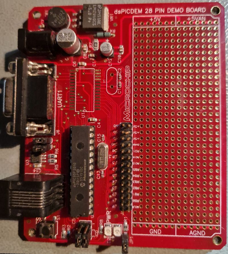
Microchip dsPIC30F 28 Pin Demo Board
dsPIC30F 28 PIN DEMO BOARD +5V +5VAN VR1 LM2540CS -5.0 P+ MICROCHIP UART1 U1 C1 C2 C10 C6 C9 C11 C12 J6 U3 C14 C15 C13 Y2 U2 -20ISF3010 dsPIC30F RB0 bis RB7 RB1 RB2 RB3 RB4 RB5 RB6 RB7 RC13 RC14 RC15 +5V
in „[V] ältere Demoboards PIC, NEC und Motor“ · Markt · · Platinenfotos
-
PDF
J-FET_J112.PDF
• High speed switching 3 d g s • Interchangeability of drain and MAM042 source connections • Low R DS ont zero gate voltage PINNING 1 = gate Fig.1 Simplified outline and symbol, TO-92. 2 = source 3 = drain Note: Drain and source are interchangeable. QUICK REFERENCE DATA J111 J112 J113 Drain-source voltage
in „J-FET J112 als Konstantstromquelle: Wie berechnen?“ · Analoge Elektronik und Schaltungstechnik ·
-
PDF
Tiny15L.pdf
0.195) 3.81(0.150) 2.92(0.115) 2.92(0.115) 0.381(0.015)MIN 0.559(0.022) 0.356(0.014) 1.78(0.070) 1.14(0.045) 8.26(0.325) 7.62(0.300) 0.356(0.014) 1.524(0.060) 0.203(0.008) 0.000(0.000) 10.90(0.430) MAX *Controlling dimension: Inches REV. A 04/11/2001 9 1187DS–12/01 8S2 .020(.508) .012(.305) .213(5.41
in „Frequenzschalter“ · Mikrocontroller und Digitale Elektronik ·
-
PDF
Product_preview_LPST096096A00-T4__Rev_0.0_.pdf
0 0 1 * * VS1 VS0 VS : Booster control clock setting Panel duty& scan 0 1 1 0 0 0 1 0 0 1 0 * SHI DS1 DS0 SHIFT : Common shift direction set direction [2H] FT DS1,DS0 : duty ratio setting Oscillator RF control RF : control the feedback resistor [3H] 0 1 1 0 0 0 1 0 0 1 1 CKS RF2 RF1 RF0 of oscillator
in „O-LED Display von SMI“ · Mikrocontroller und Digitale Elektronik ·
-
Datei
VFD_2_20.A51
_BUFSIZE EQU 20 _ClearScr EQU 1Fh ;**************************************** DSEG at 10h curState: ds 1 ;10h Byte11: ds 1 StrLen: ds 1 ;12h chksum: ds 1 ;13h RecPtr: ds 1 ;14h RecPtr CursorPos: ds 1 ;15h LinePtr RecBuffer: ds _BUFSIZE+1 ;16h Line1: ds _BUFSIZE ;2Bh Line 1 Line2: ds _BUFSIZE ;3Fh Line 2 StackP: ds 1 ;*********************************** CSEG at 0 AJMP Init org 3h RETI org 0Bh RETI org 13h RETI org 1Bh RETI org 23h LJMP Serial_IRQ ;_0023 ;*********************** org 30h Init: ;_0030: MOV SP, #StackP
in „VFD "Kundendisplay"-Ansteuerung“ · Mikrocontroller und Digitale Elektronik ·
-
PDF
Techniques_for_Robust_Touch_Sensing_Design_AN1334.pdf
sensing PCB, should be considered potential sources of ESD. Example: A mechanical power button board. DS00001334B-page 14 2010-2013 Microchip Technology Inc. AN1334 Finally, the third coupling path is the amount of Although not ideal for low-power applications, high DD additional capacitance to earth
in „Wie realisiert man Sensortasten?“ · Analoge Elektronik und Schaltungstechnik ·
-
PDF
Infineon-IPP_B_I80N04S4_04-DS-v01_00-en-1518478.pdf
GS=0V - 0.02 1 µA VDS=18V, V GS=0V, 2) - 1 20 Tj=85°C Gate-source leakage current IGSS VGS =20V, V DS=0V - - 100 nA Drain-source on-state resistance R DS(on) VGS =10V, ID=80A - 4.3 4.6 mΩ V =10V, I =80A, GS D - 3.9 4.2 SMD version Rev. 1.0 page 2 2010-04-06 IPB80N04S4-04 IPI80N04S4-04, IPP80N04S4-04
in „Hilfe bei Halbbrückenschaltung benötigt“ · Analoge Elektronik und Schaltungstechnik ·
-
PDF
drm001.pdf
case _13BIT : // 13bit resolution, 0...8191 ds_adjust_ptr = &ds_adjust[5]; break; case _14BIT : // 14bit resolution, 0...16383 ds_adjust_ptr = &ds_adjust[6]; break; case _15BIT : // 15bit resolution, 0...32767 ds_adjust_ptr = &ds_adjust[7]; break
in „AVR ATTiny84A mit C++ Werte an bestimmte Speicherstelle schreiben“ · Mikrocontroller und Digitale Elektronik ·
-
Datei
main.c
der Sensoren // Position 0-4 eig. ID, Pos. 5+6 ist die Temperatur, Pos. 7 CRC-Byte PROGMEM uint8_t DS18B20IDs[MAXSENSORS+1][OW_ROMCODE_SIZE] = { OW_ID_T01, // 1. DS18B20 OW_ID_T02, OW_ID_T03, OW_ID_T04, OW_ID_T05, OW_ID_T06, OW_ID_T07, OW_ID_T08, OW_ID_Last }; // Endmarker uint8_t auslesen = 0; // 0
in „AVR NET IO RoBue 1.5 Automatischer Ablauf“ · Mikrocontroller und Digitale Elektronik ·
-
PDF
MX26LV400__2_.pdf
DESCRIPTION 48 TSOP (Standard Type) (12mm x 20mm) SYMBOL PIN NAME A0~A17 Address Input A15 1 48 A16 A14 2 47 BYTE# Q0~Q14 DataInput/Output A13 3 46 GND A12 4 45 Q15/A-1 Q15/A-1 Q15(Wordmode)/LSBaddr(Bytemode) A11 5 44 Q7 A10 6 43 Q14 CE# ChipEnableInput A9 7 42 Q6 A8 8 41 Q13 WE# Write Enable Input NC
in „falsche u-boot nand geflasht,J-Tag möglichkeit für Flytouch2?“ · Mikrocontroller und Digitale Elektronik ·