': C:\source/mmc.c:140: undefined reference to `outb' mmc.o(.text+0x28):C:\source/mmc.c:142: undefined reference to `inp' mmc.o(.text+0x44): In function `Write_Command_MMC': C:\source/mmc.c:106: undefined
text+0x27c):C:\source/mmc.c:169: undefined reference to `outb' mmc.o(.text+0x28c):C:\source/mmc.c:140: undefined reference to `outb' mmc.o(.text+0x298):C:\source/mmc.c:142: undefined reference to `inp' mmc.o
programmiere: http://www.youtube.com/watch?v=_ZL-YNOH_jA das hier sind MEINE Makefile und main.c: Makefile main.c -> nicht PD6 sondern PB1 das hier ist er avrdude-error: avr-gcc -Wall -Os -DF_CPU=16000000 -mmcu=atmega8 -c main.c -o main.o avr-gcc -Wall -Os -DF_CPU=16000000 -mmcu=atmega8
avrdude -c avrisp -P COM3 -b 19200 -p m328p -v -v Hier: [code] avrdude: Version 5.10, compiled on Jan 19 2010 at 10:45:23 Copyright (c) 2000-2005 Brian Dean, http://www.bdmicro.com/ Copyright
= ; AD converter with ASCII logging to PC via serial port ; - build in software clock ; - ATMEGA32 at 16 Mhz ; (c) A Brussee march 2006 ; ========================================================================== .include "m32def.inc" ;=================================================================
provides power ratings from 0.5 W to 6 W at 70°C. The series supports tolerances to 0.1%, TCR as low as 25 ppm/°C, a 50 ohm to 30.1 kilohm resistance range, and operation from -55°C to +155°C. Performance testing reinforces its suitability for long service life: resistance shift is specified at ±1% after 1000 hours of endurance, ±0.4% after 1000 hours of damp heat with load, and ±0.2% after 100 thermal-shock cycles from -55°C to +150°C. [/c] 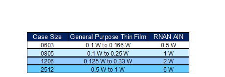 Bildquelle: Stackpole
4KBytes internal SRAM – Write/erase cycles: 10,000 flash/ 100,000 EEPROM – Data retention: 20 years at 85°C/ 100 years at 25°C (1) – Optional boot code section with independent lock bits In-system programming by on-chip boot program True read-while-write operation – Programming lock for flash program
range, otherwise specifications are At T5°C. (Note 4) SYMBOL PARAMETER CONDITIONS MIN TYP MAX UNITS LOGIC INPUTS (CLK, OE, SHDN, MUX) VIH High Level Input Voltage VDD = 3V ● 2 V VIL Low Level Input Voltage VDD = 3V ● 0.8 V I Input Current
4 23H S COM35 COM28 253 D4 B B 24H : COM36 COM27 84 D5 B B 25H ] COM37 COM26 254 D6 B B B 26H = COM38 COM25 83 0 D7 27H COM39 COM24 255 D0 B B 28H COM40 COM23 82 D1 B B B 29H COM41 COM22 256 D2 B B B 2AH COM42 COM21 81
eher, weil sie relativ geringe Toleranzen aufweisen. Bei Interesse könnte ich das auch noch mit BF245C und BF256B probieren. Allerdings sind die auch alle aus einer Charge. Gruß, Bernd
U1 = EF183 U2 = EC(C)84 U3 = E(C)C84 U4 = EC92 oder EFxx später: U4+U5 = ECL80
www.cyti.com.tw CY2890 F02 Datasheet Version 2.4 cyti Confidential, DO NOT COPY 4. Pin Assignment K 1 K I I C S D O C 0 1 2 3 4 5 0 1 2 R R D V V D H R R R R R R G G G 48 47 46 45 44 43 42 41 40 39 38 37 36 35 34 33 RI2 49 32 GO3 RI3 50 31 GO4 RI4 51 30 GO5 RI5 29 52 BO0 RI6 53 28 BO1 RI7 54 27 BO2 GI0 55 26
prescaler assigned to Timer0 (PSA = 0) ; -----110 prescale = 128 (PS = 110) option ; -> increment at 256 Hz with 32.768 kHz input ;***** Main loop main_loop ; TMR0<7> cycles at 1Hz, so continually copy to LED (GP1) rlf TMR0,w ; copy TMR0<7> to C clrf temp rlf temp,f ; rotate C into temp rlf temp,w ;
15 34 P3.6/UCA1TXD/UCA1SIMO P1.4/SMCLK 16 33 P3.5/UCA0RXD/UCA0SOMI 17 18 19 20 21 22 23 24 25 26 27 28 29 30 31 32 0 1 2 2 3 4 1 2 5 6 7 K A L E O / T/T / C C C A/ T/ C AC C C S S S I . 6.7 . K K 0 0 1 /S K 0 0 0 0 0 0 1 1 1 L L AT C C O L T C C C C A P P P C / N T 3 4/ / 2 7 / / / / C . A U 2 2. 2 C
ANS 1523-0005 Lithium-Thionylchlorid Batterie ER26500 / C Maße Ø 26,5 mm Höhe 50 mm 3,6Volt ??
interface. https://www.eevblog.com/forum/repair/quick-repair-project-marconi-2024/?all da wird ein AT28C256 erwähnt, kann aber sein, dass es dabei um den 2025 geht. Und ein Level2-Passwort, wie man es herausfindet (2025?) Hier ein Foto der Rückseite, aber ohne Batteriehalterung: https://www.rigpix.com
von einem Initvalue von 0b00 aus. (Schlechte Idee) D.h. der Befehl oben erzeugt 0b01 Uses SOT0_0 at the input pin of MFS ch.0 SOT. Uses SOT0_0 at the output pin Aufgrund des obigen Kommentares gehe ich auch davon aus, dass SIN0S auf default angenommen wird. [bit5:4] SIN0S: SIN0 Input Select bits Selects input for SIN0 0b00 Uses SIN0_0 at the input pin of MFS ch.0 SIN. [Initial value]
10 Receive data USB_VBUS 24 USB power supply USB Interface USB_DP 27 USB data line positive USB_DN 28 USB data line negative Note: Hardware flow control is disabled by default. The AT command “AT+IFC=2,2” can enable hardware flow control .The AT command “AT+IFC=0,0”can disable hardware flow control.
Composer Studio, which includes a mini operating system > called DSP/BIOS. Additionally, a department at the Chemnitz University of > Technology has developed preliminary support for the TMS320C6x series in > the GNU Compiler Collection.[4] > In November 2007 TI released part of its toolchain as
TMS320VC5509A konnte Mann z.B. im QFP-144-Package samplen. (TMS320VC5509APGE) Vorteil: Der DSP hat 256 kByte/128 kWorte schon im Gehaeuse. Entsprechend minimal kann die Aussenbeschaltung ausfallen. Booten kann er von diversen Quellen, u.a.: - I2C-EEPROM - SPI-Flash - MMC/SD - USB (FS im Client-Modus
the optimal speed. // Other output doesn't need to be that speedy. // :[0, 2, 4, 8, 16, 32, 64, 128, 256] #define TX_BUFFER_SIZE 0 // Host Receive Buffer Size // Without XON/XOFF flow control (see SERIAL_XON_XOFF below) 32 bytes should be enough. // To use flow control, set this buffer size to at least
support for multiple new devices ;* V2.1 98.10.26 (mlund) New date marking. ;* Removed support for AT90S1200C. ;* Added support for AT90S4433A. ;* V2.0 98.01.06 (mlund) ATmega103 support ;* V1.7 97.11.06 (mlund) Universial command (':') implemented. ;* Releases all pins when not in ;* programming mode
Converter und Hterm läuft alles.Im Terminal bekomme ich dies angezeigt: MC535-MONITOR/BASIC V1.26c (C) PHYTEC Messtechnik 1989 MONITOR MODE # Nach der Eingabe von Help erscheint dieses: #HELP memory display modify fill verify bit: >DB range >EB address >FILLB
Auf U10 ist ein fest verbauter 62256 in SMD.U8 halt der Code Eprom.Und U11 hat einen 28c256 EEPROM. Schreib und lesezugriff ist ab Adresse 8000H möglich. Aber auf Seite 53 steht ja das Speichermodell. Mein Board ist auf MODE 0, Seltsam finde ich das dort der EEPROM U11 mit einem Adrssbereich
High", cursor blink is on, that performs alternate between all the high data and display character at the cursor position. When B = "Low", blink is off. Alternating display Every 64 frames Cursor z Cursor or Display Shift RS R/W DB7 DB6 DB5 DB4 DB3 DB2 DB1 DB0 0 0 0 0 0 1 S/C R/L X X ¾ S/C: Screen/Cursor
High", cursor blink is on, that performs alternate between all the high data and display character at the cursor position. When B = "Low", blink is off. Alternating display Every 64 frames Cursor z Cursor or Display Shift RS R/W DB7 DB6 DB5 DB4 DB3 DB2 DB1 DB0 0 0 0 0 0 1 S/C R/L X X ¾ S/C: Screen/Cursor
steht so in jeder Literatur zum >> Thema Computerarchitektur. Für nen Full-Adder kann man bis zu 28 >> Transistoren rechnen und so ne poplige 8 bit CPU kommt mit weniger als >> 10000 Transistoren aus. Eigentlich keinerlei Abweichung, weil 8*8*28 = 1792 und damit wie erwartbar im oberen Bereich
Profile Construction Low Profile Construction Manual Reset Construction Options shown: 90° – 1/4” Q.C. terminals with 4 Post Options shown: 45°– 1/4” Q.C. terminals Options shown: Flat 1/4” Q.C. terminals with Surface mount flange with 4 post and flat Al cup Airstream mount cup ø3.72 (.147) Ref. 30.0
Profile Construction Low Profile Construction Manual Reset Construction Options shown: 90° – 1/4” Q.C. terminals with 4 Post Options shown: 45°– 1/4” Q.C. terminals Options shown: Flat 1/4” Q.C. terminals with Surface mount flange with 4 post and flat Al cup Airstream mount cup ø3.72 (.147) Ref. 30.0
sind als die "leicht" erhöhten Preise von Conrad. Ein kleines Beispiel: Zeitech: RIGOL DS1022C DSO 859,00 EUR (19% Mws) RIGOL DS1102C DSO 1.329,00 EUR(19% Mws) Conrad.AT: RIGOL DS1022C DSO 599,00 EUR (20% Mws) RIGOL DS1102C DSO 1199,00 EUR(20% Mws) @ Matthias Ich kann
>J310 Den hatte ich vor dem BF256C probiert, war aber zu lahm, wird ja auch nur für VHF empfohlen. >BF998 bis 1GHz bei Farnell Farnell zählt für mich nicht unter "leicht zu beschaffen", aber ich hab den BF910 (ebenfalls Dual Gate
) *) at / beiTI = 10 mA Sperrspannung at / bei WM at / beiPPM(10/1000 µs) unidirectional bidirectional V BR[V] V WM[V] ID[µA] V CV] IPPMA] P6KE6.8 P6KE6.8C 6.8 ± 10% 6.12...7.48 *) 5.5 1000 10.8 58.0 P6KE6.8A
TPS65217C and the processor. It is a cut from the PDF form of the schematic and reflects what is on the schematic. Figure 28 Power Processor Interfaces When voltage is applied, DC or USB, the TPS65217C connects
High", cursor blink is on, that performs alternate between all the high data and display character at the cursor position. When B = "Low", blink is off. Alternating display Every 64 frames Cursor " Cursor or Display Shift RS R/W DB7 DB6 DB5 DB4 DB3 DB2 DB1 DB0 0 0 0 0 0 1 S/C R/L X X # S/C: Screen/Cursor
100 Bytes für eine Adresse ist mehr als geizig. Was ja die Praxis bewiesen hat. Ich persönlich hätte 256 Bytes genommen. Irgendwo muss ja mal Schluß sein ;)
Prozessor ist ein PIC18F67J60 (Takt: 25MHz), an dem 3 Speicherbausteine angeschlossen sind: 2 x 23K256 SRAM und 1 x AT45DB081S-SU Flash-Speicher. Der MP3-Datenstrom wird mit Hilfe eines VS1011e dekodiert und an einen digitalen TPA2008D2 NF-Verstärker weitergegeben. rhf
August 2004 AS7C34098A ® 3.3 V 256 K × 16 CMOS SRAM Features • Pin compatible with AS7C34098 • Easy memory expansion with CE , OE inputs • Industrial and commercial temperature • TTL- and CMOS-compatible, three-state
die parasitären Cs gibt es ja auch noch... Wie kann man denn ein Ladderfilter für bestimmte C-Werte optimieren? Es gibt doch bestimmt so eine Art "Schablone" für die Bauteilwerte (z.B. C2 = 1,2 * C1, C3 = 8 * C1 oder so). > Beim DG-Mosfet kommt > das Eingangssignal und das Oszillatorsignal
ab. Trotzdem kann man damit Receiver bauen, die funktionieren. > ein Ladderfilter für bestimmte C-Werte optimieren? > Es gibt doch bestimmt ein Schema > z.B. C2= 1,2 * C1, C3 = 8 * C1 oder so Da verweise ich nochmal auf ihn. http://www.giangrandi.ch/electronics/crystalfilters/xtalladder.html
erreichbar. Hast Du eigene Zahlen, die mehr als 2..2,5 belegen? Wasser/Wasser Wp mit Wärmequelle 10°C und Heizwasser 35°C, da hat man locker einen COP von 4! Ich hab eine Sole-WP 3,5kW elekt.: Bei einer SoleTemp von -5°C gibt das bei 35°C Heizwasser 13,5 kW, bei SoleTemp von -0°C sind es dann 14,2kW
aus Süddeutschland Eher zwischen Hanau und Bremen. https://de.wikipedia.org/wiki/Deutsche_M%C3%A4rchenstra%C3%9Fe
der Versorgungsspannung zu unterdrücken. Hier die Liste der benötigten Bauteile: R1 Widerstand 10k C1 Keramikkondensator 47p C2 Keramik- oder Folienkondensator 100n Stiftleiste 6-polig Mikrocontroller ATmega8 oder AT90S4433 (kann auf http://shop.mikrocontroller.net/ bestellt werden) Quarzoszillator
bist du trotz allem nicht sicher vor Überwachung: http://www.zeit.de/digital/datenschutz/2013-12/30c3-nsa-methoden Bleibt doch nur, den Raum komplett zu schirmen...
Netzfilter, an die alle Geräte angeschlossen werden. 2. http://www.amazon.de/Abgeschirmtes-Kaltger%C3%A4tekabel-EMV-schwarz-2m/dp/B000W9LSLO/ref=sr_1_2?ie=UTF8&qid=1388611523&sr=8-2&keywords=kaltger%C3%A4tekabel+EMV Abgeschirmtes Kaltgerätekabel, ist zwar maßlos überteuert, aber immer noch besser
F1 Data 22 SSTL18 Class 1 DDR2_DQ22 AF10 U25 pin F9 Data 23 SSTL18 Class 1 DDR2_DQ23 AE13 U25 pin C8 Data 24 SSTL18 Class 1 DDR2_DQ24 AC8 U25 pin C2 Data 25 SSTL18 Class 1 DDR2_DQ25 AH7 U25 pin D7 Data 26 SSTL18 Class 1 DDR2_DQ26 AG8 U25 pin D3 Data 27 SSTL18 Class 1 DDR2_DQ27 AH8 U25 pin D1 Data 28
to the 120kHz carrier frequency. The primary of the transformer, in series with capacitor C3, is directly across the power-line. Capacitor C3 presents a low impedance at the carrier frequency but a high impedance at the power-line frequency. The carrier signal is passed but excessive 50Hz (
to the 120kHz carrier frequency. The primary of the transformer, in series with capacitor C3, is directly across the power-line. Capacitor C3 presents a low impedance at the carrier frequency but a high impedance at the power-line frequency. The carrier signal is passed but excessive 50Hz (
applied to theTVS without operation V Breakdown Voltage -- Maximum voltage that flows though theTVS at a specified test current (I ) BR T V Clamping Voltage -- Peak voltage measured across theTVS at a specified Ippm (peak impulse current) C IR Reverse Leakage Current -- Current measured at V R VF Forward
Microchip product came forth. Not only does Microchip have great processors at affordable prices, but they have other support devices to support the design. Having worked with Microchip products in the past, I know they have a great support team in place when assistance is required
google: zweiter eintrag: http://thomaskropf.at/index.php?option=com_content&task=view&id=19&Itemid=28 mal wieder einer der zu faul zum selber suchen ist
= 1H/3H ; 3 = 3L/1L X 12 ; ... ; 48 = 1H ; 49 = 31L ; Familiencode: a 0 b 1 c 2 d 3 e 4 f 5 g 6 h 7 i 8 j 9 k A l B m C n D o E p F Gerätenummer: (Gerät+Gruppe*4) Gerät: (x1) 1 0 2 1 3 2 4 3 Gruppe: (x4) 1 0 2 1 3 2 4 3
