Empfehlungen != Grundsatz-Diskussion. Ein L200 würds auch tun ;) Klaus.
Klaus R. schrieb im Beitrag #8033756: > Empfehlungen != Grundsatz-Diskussion. > > Ein L200 würds auch tun ;) Nein, ein L200 tut es nicht. Der TO hat nach Empfehlungen für ein Netzteil gesucht, nicht nach möglichen Bauteilen oder Bausätzen.
30C to 60C Self Discharge: ~1% / year 2.50 (0.098) 2.20 (0.087) 20.00 (0.787) Safety: 2.18 (0.086) Ref. 8.00 (0.315) 19.70 (0.776) 1.88 (0.074) Ref. Minimum (1) KEEP OUT OF REACH OF CHILDREN. Swallowing may lead to serious injury or death in as little as 2 hours due to chemical burns and potential perforation of the esophagus. Immediately see doctor; have doctor phone (800) 498-8666. 0.03 (0.001) Minimum Ref. edge of crimp, whichever is higher.)(2) Battery compartment design. To prevent children from removing 0.20 (0.008) Maximum Ref. batteries, battery compartments should be designed with one of the Permissible
successed The above parameters are a decimal 2.ERROR=<Error_Code> — number. —failed The default:400,200,400,200 Command 26: Inquires/set—— Security and encryption mode command answer parameter TEL:86-0755-26509941 WEB:www.bolutek.com Page 10 of 21 BOLUTEK BLK-MD-BC04-B BLUETOOTH MODULE AT COMMANDS AT+
3.000V SELECTION GUIDE (VRE118) and ±3.000V (VRE119) outputs with Type Output Temperature Max. Volt ±0.200 mV initial accuracy and temperature Operating Range Deviation coefficient as low as 0.6 ppm/°C over the full military temperature range. This improvement in VRE117C +3.0V -25°C to +85°C 200 µV accuracy
parameters Project Test conditions Norm 75%RH 25℃ 10KΩ Max Resistance value 93%RH 25℃ 70KΩ Max 100%RH 60℃ 200KΩ Max Response speed 25℃,60%RH → 60℃,100%RH Less than 5 seconds Temp. cycling -40℃,30 minute ~ 85℃,30 minute 5 cycles relative humidity resistance value High temperature 85℃,2000 hour Hypothermia -40
configures the time for sending LCP echo request. The unit of time is 25ms. Ex) in case that PTIMER is 200, 200 * 25(ms) = 5000(ms) = 5 seconds PMAGIC (PPP Link Control Protocol Magic number Register) [R/W] [0x001D] [0x00] PMAGIC configures the 4bytes magic number to be used in LCP echo request. Ex) PMAGIC
) 90 ( ( c c i 85 i 85 f f E 80 VIN=3V E 80 VIN=5V VIN=3.7V VIN=12V 75 75 VIN=4.2V VIN=16V 70 70 0 200 400 600 800 1000 0 100 200 300 400 500 Load Current(mA) Load Current(mA) Line/Load Regulation Line/Load Regulation VOUT=5V VOUT=18V 5.5 19 V V e e l l V 5 V18 u u u u O VIN=3V O VIN=5V VIN=3.7V VIN=12V VIN=4.2V VIN=16V 4.5 17 0 200 400 600 800 1000 0 100 200 300 400 500 Load Current(mA) Load Current(mA) Operation Frequency vs. Input Voltage Operation Frequency vs. Input Voltage VOUT=5V VOUT=18V 1.3 1.3 1.2 1.2 z z H H y y n 1.1
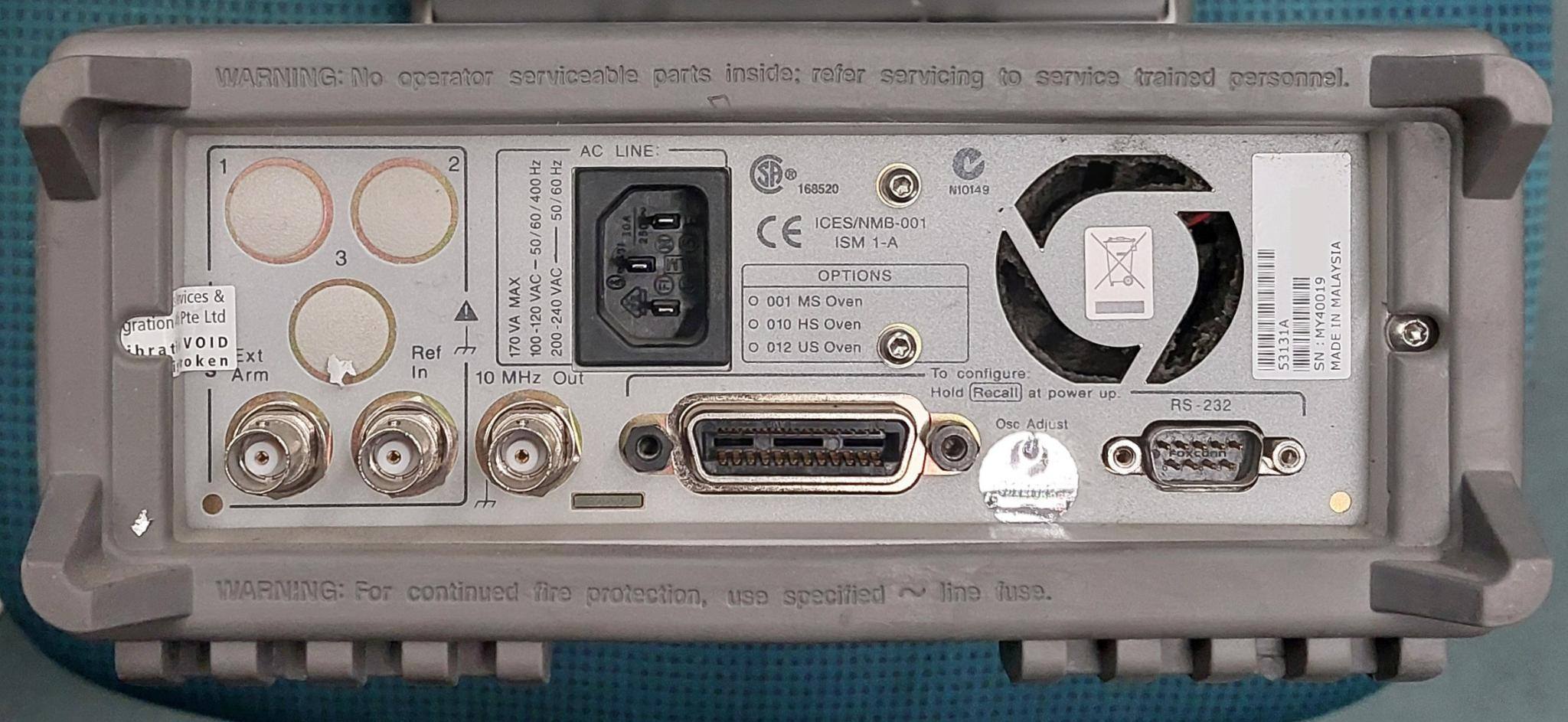
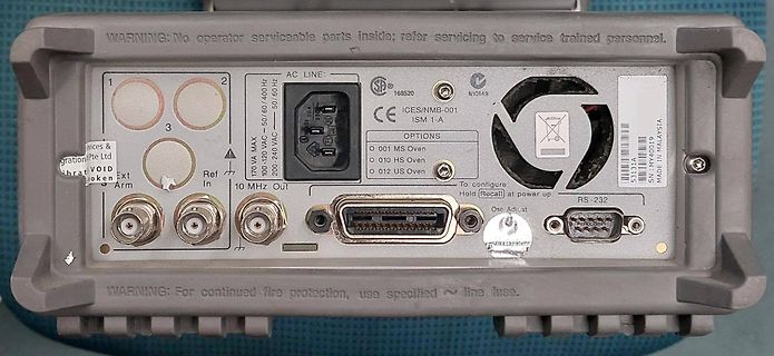
WARNING: No operator serviceable parts inside; refer servicing to service trained personnel. AC LINE: 170 VA MAX 100-120 VAC -50/60 Hz 200-240 VAC. CE ICES/NMB-001 ISM 1-A. OPTIONS: 001 MS Oven, 010 HS Oven, 012 US Oven. To configure, Hold Recall at
below. Table 4. FUNC pin functions FUNC external resisto Set application voltage Hang in the air 5V 200K 9V 120K 12V 51K 15V Grounding 20V The functions of FS312BH and FUNC pins are shown in the table below. Table 5. FUNC pin functions FUNC external resisto Set application voltage Hang in the air 5V 200K
High-contrast color coding Available with two, one, or on housing aids identification no mounting holes Refer to ISO 20934 –Type SF51 Applications Cars / SUVs Buses Additional Information Trucks Watercraft as approved by Littelfuse Offroad vehicles See Disclaimer Notice Resources Samples Specifications Voltage
DLS card, the measuring circuit is in good working order. Display on FLA remote control and monitor P200 f (Hz) v (km/h) settings U ss (V) f (Hz) Required min max Required min max 4 200 200 195 205 7.2 7.0 7.4 8 400 400 393 407 14.4 14.1 14.7 16 1600 1600 1581 1619 57.6 56.9 58.3 32 6400 6400 6333 6467
mV 102 mV V (RCH) Recharge threshold V − V − V − BQ2057T and BQ2057W O(REG) O(REG) O(REG) V 196 mV 200 mV 204 mV CHARGE-RATE COMPENSATION (AutoComp) V (BAT)0.3 V≤ VCC ≤ VCC(max) BQ2057, BQ2057C, 1.87 2.2 2.53 BQ2057T, BQ2057W G (COMP) AutoComp gain V/V V (BAT)0.3 V ≤ CC ≤ VCC(max), BQ2057T and BQ2057W
Transciever. Preise ab 3€ bis zu 8 digitale IOs bis zu 2 PWM, 10 Bit bis zu 4 ADC, 10 Bit, externe Ref. SLEEP-Mode etc. Datenblatt USB CAN Bridge. Neben der Möglichkeit mit CANable, CANdlelight, Klipper usw. einen eigenen USB-to-CAN Umsetzer zu bauen gibt es auch ein fertiges IC von Holtek Holtek HT42B536
CAN/LIN nach USB Adapter von KOPF GmbH Ab 320,- EUR PC/CAN-Interfaces von IXXAT Automation GmbH ca. 200 EUR CAN-Interfaces von Peak-System Ca. 200 EUR USB to CAN Bus Interface von EMS Dr. Thomas Wünsche Ca. 180 EUR USB-CANmodul Serie von SYS TEC electronic mit Unterstützung von 1, 2, 8, oder 16 CAN Kanälen
einschlägigen Chinaversendern zu haben. Als Grundplatte habe ich eine gerade vorhandene Messingplatte (200mm x 140mm x 10mm) verwendet. Kann natürlich auch eine ordinäre Eisenplatte sein. Die Platte sollte nicht zu leicht sein und am Unterboden mit kleinen selbstklebenden Silikonfüßchen gegen verrutschen
https://www.amazon.de/Fixpoint-Platinenhalter-Best%C3%BCcken-Leiterplatten-Platine/dp/B000LB4PWM/ref=sr_1_1_sspa? Das es gute Selbstbaulösungen gibt ist unumstritten. Bisher hatte ich nur gekauftes Zeugs. PS: Wir sind hier nicht im Kindergarten.
stereo FM transmitter designed for portable audio/video players, automotive accessories, cell 50/100/200 kHz step sizes phones, and GPS personal navigation devices. The • 50/75 s pre-emphasis QN8027 covers frequencies from 76 MHz to 108 MHz in 50/100/200 kHz step sizes for worldwide FM band support. •
transponder in the car immobilizer industry. It is used by at least 34 car makes and fitted in more than 200 different car models. Hitag2 uses a propriet- ary stream cipher with 48-bit keys for authentication and confidentiality. This article reveals several weaknesses in the design of the cipher and presents
012 Cl—I 01 013 vcOOuT Cl —2 5 FYI 014 RXI 014100 C1 1 1MHz RX2 CD4060 S T 1 ( X ) - ZENER Rege isp, ref f ST2 II 1C3 12 9 01 I 02 RESET,: : 0 0 n 03 Pt V 04 ST3 05 5T7 +5V bis +15V 06 f out 07 C5 + c C 7 1 c 08 09 010 SIB OCn lOOn 011 k e r jk e r Ik e r 012 Bud 2: Schaltbild der mit dem CD4046 aufgebauten
darüber geht der Ausgang vom Opamp auf 1,35V und clampt bis ca 3V. Der Mosfet kocht bei etwas über 200mA, wie gehabt
was auch passt. Die Sache mit den Transistoren ist definitiv ein Backup. Ist ja die gängige Art, Ref plus kleinen PNP und größeren NPN. Gegebenfalls Ref plus PNP. Aber wenn es sich bei PNP und NPN ähnlich verhält wie bei NMOS und PMOS (N-Channel günstiger, besser), dann eher kleiner PNP und etwas größerer
MAX UNITS Zero Input Reading VIN = 0V, -000.0 ±000.0 +000.0 -000.0 ±000.0 000.0 Digital Full Scale = 200mV Reading Ratiometric Error (Note 11) V = V 0.999 1.000 1.001 0.9999 1.0000 1.0001 Digital IN REF Full Scale = 2V Reading Linearity Over ± Full Scale (Error of -2V ≤ VIN≤ +2V - 0.2 1 - 0.5 1 Counts
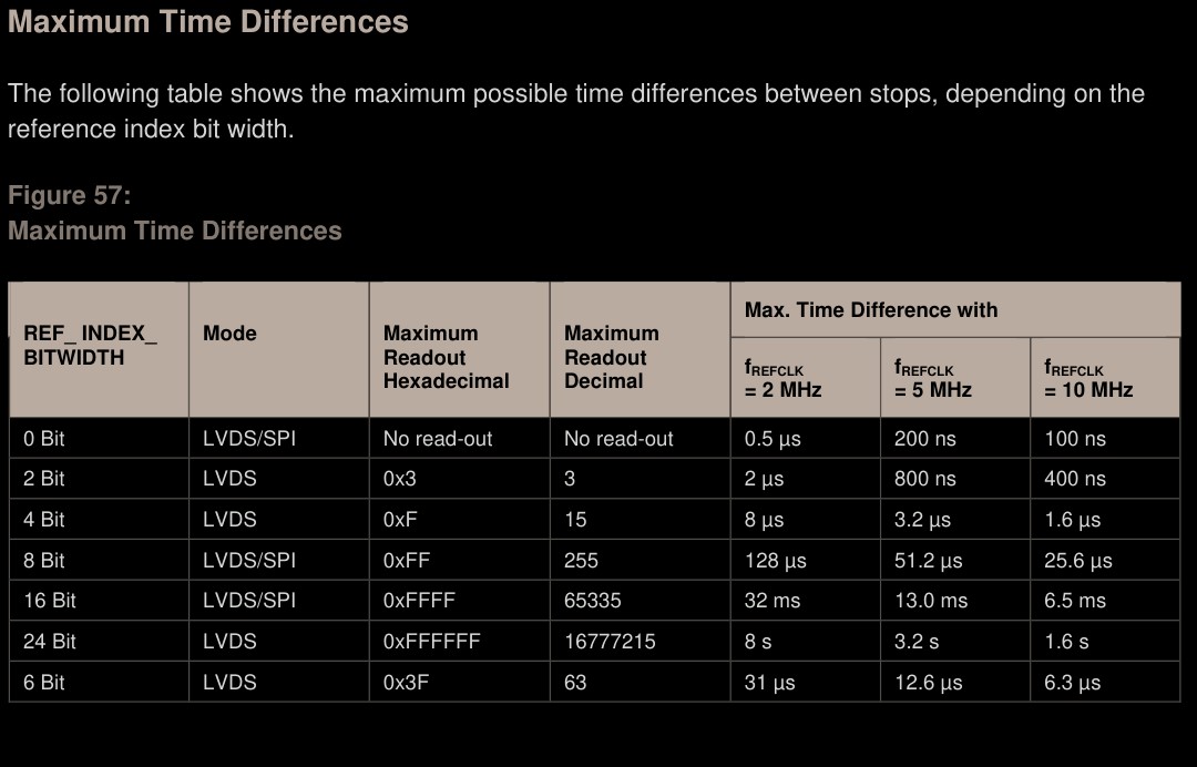
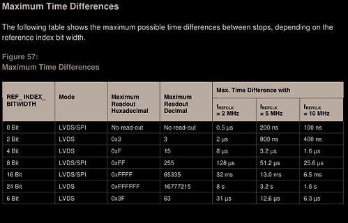
differences between stops, depending on the reference index bit width.
Figure 57: Maximum Time Differences
REF_INDEX_BITWIDTH Mode Maximum Readout Hexadecimal Maximum Readout Decimal Max. Time Difference with fREFCLK = 2 MHz fREFCLK = 5 MHz fREFCLK = 10 MHz
0 Bit LVDS/SPI No read-out No read-out 0.5 µs 200 ns
770 W 6 IQSHDN Shutdown Current VEN = 0 V 1 mA EN/PWM Pin REN/PWM − Internal pull−down resistance 200 kW VHI − Logic High Level 1.3 V VLO − Logic Low Level 0.4 V TSD Thermal Shutdown 150 °C THYS Thermal Hysteresis 20 °C ILED RSET RSET to LED Current gain ratio 25 mA LED current 100 VUVLO Undervoltage
operation can resume rec after CC exceeds V PFD (max). For more information on battery storage life refer to the application note AN1012. 14/33 Doc ID 2412 Rev 8 M48T58, M48T58Y Clock operations 6 Clock operations 6.1 Reading the clock Updates to the TIMEKEEPER registers (see Table 5) should be halted
enable (W) = high. Table 3. READ mode AC characteristics M48Z02/M48Z12 (1) Symbol Parameter –70 –150 –200 Unit Min Max Min Max Min Max t READ cycle time 70 150 200 ns AVAV t Address valid to output valid 70 150 200 ns AVQV tELQV Chip enable low to output valid 70 150 200 ns tGLQV Output enable low to output
DMX-controlled operation or stand alone operation with Master/Slave-function For extremely bright 1,200 W HMI-lamp Suitable for a projection area of 25-30 meters 2 colour-wheels with 7 different, dichroic colour-filters and white and additionally with correction-filters 3,200 K and 6,500 K Via the two
temperature coefficient 2 3 R = R eA + B T + C T + D T (1) T = temperature deviation, T ref –1 then: T = ---------- T = A + B ln------+-C ln 2----+ D--ln3--------- (2) TCR R 1 1 R ref 1 Rref 1 R ref The temperature tolerances are plotted in the graphs on the previous page. where: A, B
man nicht selbst bauen will: https://www.femto.de/spannungsverstaerkung/?f=d&gad_source=1 HVA-200M-40-B (und einen HVA-500M-20-B falls man 20/40/60 dB haben will einfach hintereinander schalten) Das ergibt dann auch ein schönes modernes kleines und flexibles Messkonzept mit auch für heute richtig
GND 18 RST Digital input 19 PCLK Digital input 20 OE Digital input 21 ACKN Digital output Note: 1. Ref Connector: FH18-21S-0.3SHW (HIROSE). 3 2150B–BIOM–09/03 (1) Figure 2. COB with Flex Flex with metallizations up Flex with metallizations down Figure 3. Flex Output Side Flex Output (FingerChip Connector
GND 18 RST Digital input 19 PCLK Digital input 20 OE Digital input 21 ACKN Digital output Note: 1. Ref Connector: FH18-21S-0.3SHW (HIROSE). 3 5364A–BIOM–11/03 (1) Figure 2. COB with Flex Flex with metallizations up Flex with metallizations down Figure 3. Flex Output Side Flex Output (FingerChip Connector
200-- - H P-Teeilenu mer 0 2-5952-7522. Rep araatur-Serviceleistungen b ei Stör fällle T reten ne m H P 3131A/132A2A innerhalbb v on drei ahrenn n ach dem ursprünglichenen Verkaufsdatumm F ehler uf, wird
0.5 V + 0.5 V SS(PVSS) DD(SVDD) P tot total power dissipation per package; and VDDD in shortcut - 200 mW mode T junction temperature - 100 C j V ESD electrostatic discharge voltage HBM; 1500 , 100 pF; - 2000 V JESD22-A114-B MM; 0.75 H, 200 pF; - 200 V JESD22-A114-A Charged device model; JESD22-C101

 Bild
Bild
 Bild
Bild
 Bild
Bild
 Bild
Bild
 Bild
Bild