-
PDF
hw1005_hw1007_CH1_Input_Circuit.pdf
PIC0PIC0101401 2 PIC0029SN74HC595N SELFCAL +12A -5A GND O09 1 GND CALOUT CALOUTL C01_60 C01_7 C I9 PIC01 L2P 03L5P 06 P 08 GND PIC010602 PIC010701 GND010702+12F1C1 PIC0101302 PGND101301 INRCLK 2.2pF01C12 RL01_202 100nF 100nF 10uF131 INCLKA 33R2 - 60/100MHz UD2-4.5NU P2P D0 INLTCH1 J100 hw1007 >= Jan 2012
-
PDF
BK4802N_Datasheet_V1.1_EN.pdf
PIN Voltage Frequency Channel PIN Voltage Frequency No. B0/C2/C1/C0 (MHz) No. B0/C2/C1/C0 (MHz) 1 L / L / L / L 27.125 9 H / L / L / L 422.05 2 L / L / L / H 27.145 10 H / L / L / H 434.125 3 L / L / H / L 40.665 11 H / L / H / L 433.075 4 L / L / H / H 40.685 12 H / L / H / H446.00625 5 L / H / L / L 49.86 13 H / H / L / L 448.7625 6 L / H / L / H 49.89 14 H / H / L / H 462.5625 7 L / H / H / L 409.75 15 H / H / H / L 462.6625 8 L / H / H / H 433.92 16 H / H / H / H 477.325 Proprietary and Confidential
in „Tranceiver Chip RDA1846 Erfahrungen Selbstbau“ · HF, Funk und Felder ·
-
PDF
Bluno_beetle_V1.0_layout_top.pdf
COJ14 COJ17 COJ4 O5 COJ6 COJ10 PJ01401 A01 P41 51 J1 PA01001 COPWR COTX COLINK OL CORX2A01AIR L1 A1 1R30O0 PX1 R1P02 N1 P71C7 L2 A2 1R60O8 PX2 R2P01 A02 N2 P72 CO4 COROW1 COIC5 42A1OR4 42C1I221 C1 AICC0187 P20 I03C2C3 C7IC5026P54C5015A02 PAIC5029PAIC5012A015 PAJP101 PD02 PAIC5031PAIC50100 O1 PAJCOR3 O1 PAIC5032PAIC509 A16 PAJP10402A0O1 PIIC5078 O3A02 PAJPR0ACR102 COCP102A04 A03 19 C71 A01 R1ACP22 O18PC0A01 A02 P81 O1L2A0P21O2 A82 OC8 COR12P21 COBOOT P82 C2 R1A2 PS01 AS2AO02 BO1 CR6 O4 C1 CORST PAJ1501 P01 P31 11 11 PAJ1101 COJ15 COJ9 COJ13 COJ1 COJ16 COJ11
in „Bluno Beetle mit CC2540 - Low Power?“ · Mikrocontroller und Digitale Elektronik ·
-
PDF
176001-da-01-en-ic_lm317t.pdf
L M November 1997 1 7 L M 3 LM117/LM317A/LM317 1 7 3-Terminal Adjustable Regulator A age, supplies of several hundred volts can be regulated as General Description long as the maximum input to output differential
-
PDF
176001-da-01-en-IC_LM317T.pdf
L M November 1997 1 7 L M 3 LM117/LM317A/LM317 1 7 3-Terminal Adjustable Regulator A age, supplies of several hundred volts can be regulated as General Description long as the maximum input to output differential
in „Spannungsregler“ · Mikrocontroller und Digitale Elektronik ·
-
PDF
LM317.pdf
L M February 1998 1 7 L M 3 LM117/LM317A/LM317 1 7 3-Terminal Adjustable Regulator A age, supplies of several hundred volts can be regulated as General Description long as the maximum input to output differential
in „Einfaches regelbares Netzteil mit LM350“ · Analoge Elektronik und Schaltungstechnik ·
-
Datei
test.c
LCD_PORT; // Status lesen LCD_CE = 1; // Chip Enable High LCD_RD = 1; // Read High LCD_STATUS &= (0x03); // Bits ausmaskieren } void lcd_status_am(void) { pd2 = 0x00; // Port 2 als Eingang LCD_CD = 1; // Commando High LCD_RD = 0; // Read Low LCD_CE = 0; // Chip Enable Low asm ("NOP"); asm ("NOP"); asm
in „Grafik-Display mit T6963C“ · Mikrocontroller und Digitale Elektronik ·
-
PDF
vcnl4040.pdf
enable / disable 0x03 H PS_CONF2 R / W 0x00 PS output resolution selection, PS interrupt trigger method L PS_CONF3 R / W 0x00 PS smart persistence, active force mode 0x04 White channel enable / disable, PS mode selection,
in „VNCL4040 Vorwiderstand?“ · Mikrocontroller und Digitale Elektronik ·
-
PDF
MC39I_AT_COMMANDS.pdf
Coefficient for base station reselection, decimal, e.g. 30 Example (response) AT^SMONC ^SMONC: 232,03,3010,4EAF,32,82,38,30,30,232,03,3010,0000,36, 88,26,18,18,232,03,3010,4EC3,32,112,23,15,15,232,03,3010,4BD A,34,90,17,9,9,232,03,3010,0000,32,99,15,7,7,232,03,2010,00C 0,35,113,9,1,1,232,03,3520,0000,32,85,8,0,0
in „DTMF mit GSM Modem auswerten“ · Mikrocontroller und Digitale Elektronik ·
-
PDF
BLDC_Controller.pdf
Induktivität 0.40uH A NFAU PIIC102 OTW BST_A PIIC1035 PCPI1 FAULT PIIC103 FAULT PVDD_A PIIC1034 PVDD L2 PWM_A PIIC104 PWM_A OUT_A PIIC1033 OUT_A0 PL0 PL0 P1 CO RESET_A PIIC105 RESET_A GND_A PIIC1032 GND_A0 600 Ohm @ 100MHz V1 PWM_B PIIC106 PIIC1031 GND_B0 PIV1 03 0R AGND NOC_ADJ 7 PWM_B GND_B 30 OUT_B0
in „Tipps Platinenlayout“ · Platinen ·
-
Datei
flap_mehrzeilig.htm
0; var gefunden=0; var zeichensatz = new Array(""," ","A","B","C","D","E","F","G","H","I","J","K","L","M","N","O","P","Q","R","S","T","U","V","W","X","Y","Z","0","1","2","3","4","5","6","7","8","9",".",",","&","!","?","-","_","Ü","Ä","Ö","ß"," "); for(var i = 0;i<zeichensatz.length;i++){ if(zeichen=
-
PDF
R-IN32M-CL_CC-Link_IE_Field_Intelligent_device_station.pdf
communication DMF(0x00) SMF(0x00) DNA Destination network number Transient2 header DS Destination node number L DID(0x03FF) H SNA Source network number SS Source node number (lower 8 bits) L SID(0x03FF) H L L1 H CT RSV(0x00) L Application side identification APS H number DATA Transient2 data area (0 to 968 bytes
in „Wie funktioniert der Interrupt- bzw. Eventaufruf?“ · Mikrocontroller und Digitale Elektronik ·
-
Datei
8x2_lcd_clock.asm
0x03 andwf v_ct1,w call l_interrupt_frame call l_check_keys call l_phase_scroll incf v_ct1,f btfsc v_prgbits,c_prgbits_ldr2 call l_test_ldr movf v_status_backup,w movwf STATUS movf v_workreg_backup,w retfie
in „Der totale Anfänger - auf der Suche nach einem Mikrokontroller“ · Mikrocontroller und Digitale Elektronik ·
-
PDF
mb506-1.pdf
SW SW D Q D Q D Q D Q D Q Output SW SW Buffer C Q C Q C Q C Q C Q OUT SW1 SW2 Divide Ratio H H 1/64 L H 1/128 H L 1/128 L L 1/256 Note: H = CC, L = open Figure 1. MB506 Block Diagram PIN DESCRIPTION Pin Number Symbol Function 1 IN Input 2 V Power Supply Voltage CC 3 SW1 Divide Ratio Control Input Selecting
in „Eingangsbeschaltung GHz-Vorteiler aus altem Sat-Tuner“ · HF, Funk und Felder ·
-
PDF
RG12864K-BIW-VBG.pdf
Description 1 VSS 0V Ground 2 Vdd 5.0V Power Supply (+5V) 3 V0 (Variable) Contrast Adjustment 4 RS H/L Data/ Instruction 5 R/W H/L Data read /write 6 E H Enable signal 7 DB0 H/L Data bus line Data bus line 8 DB1 H/L 9 DB2 H/L Data bus line 10 DB3 H/L Data bus line 11 DB4 H/L Data bus line 12 DB5 H/L Data
in „LCD U8g2 asm“ · Mikrocontroller und Digitale Elektronik ·
-
PDF
Bettgiebel_Schaltplan.pdf
ESP-12F 1 R R3 +3.3V 1 C 18 +5V +3.3V RST C GPIO0 470R R5 PS1 U1 V GPIO1/TXD 22 TXD 12k J1 F1 IRM-03-5S AMS1117-3.3 3 17 Screw_Terminal_01x03 1.A f EN GPIO2 3 1 16 3 VI VO 2 R4 GPIO3/RXD 21 RXD AC/L +Vo D 2 19 2 N 12k ADC GPIO4 1 3 14 G GPIO5 20 AC/N -Vo 1 9 CS0 GPIO12 6 C3 C4 10 7 10µF 10µF MISO GPIO13
-
PDF
CoolRoadRunnerIII-HB-2.pdf
CPU: ® ® - Intel ULV Celeron at 650MHz ® ® - Intel Pentium -III at 933MHz Cache Memory: • Celeron - L1: 16 KB instruction cache and 16 KB write-back data cache - L2: 256 KB ECC protected cache • Pentium-III - L1: 32 KB instruction cache and 32 KB write-back data cache - L2: 512 KB ECC protected cache
in „Embedded PC erkennt keine Festplatte“ · PC Hard- und Software ·
-
PDF
CS4272.pdf
Mode Stopband Rejection Figure 46. ADC Single Speed Mode Transition Band 0 0.10 -1 0.08 -2 0.05 -3 0.03 B -4 ) ( d e e t -5 d 0.00 l l m p A -6 m A -0.03 -7 -0.05 -8 -9 -0.08 -10 0.45 0.46 0.47 0.48 0.49 0.50 0.51 0.52 0.53 0.54 0.55 -0.10 0.00 0.05 0.10 0.15 0.20 0.25 0.30 0.35 0.40 0.45 0.50 Frequency
in „was ist "ATAPI channel mixing" Warum kein Ausgangssignal?“ · Mikrocontroller und Digitale Elektronik ·
-
Datei
font6x8s.c
0x00, 0x00, 0x00, 0x00, 0x00}, // SPACE {0x00, 0x00, 0x00, 0x5F, 0x00, 0x00}, // "!" {0x00, 0x00, 0x03, 0x00, 0x03, 0x00}, // """ {0x00, 0x14, 0x3E, 0x14, 0x3E, 0x14}, // "#" {0x00, 0x24, 0x4A, 0xFF, 0x4A, 0x32}, // "$" {0x00, 0x23, 0x13, 0x08, 0x64, 0x62}, // "%" {0x00, 0x36, 0x49, 0x55, 0x22, 0x50},
in „Fragen zu einem GLCD“ · Mikrocontroller und Digitale Elektronik ·
-
PDF
AD623.pdf
LargeSignalPulseResponseandSettlingTime, Figure32.LargeSignalPulseResponseandSettlingTime, G=−1(0.250mV=0.01%),C =100pF L G=−1000(5mV=0.01%),C =100pF L Rev. D | Page 12 of 24 AD623 20mV 2µs 20mV 500µs 3 6 0 0 7 7 0 0 0 0 Figure33.SmallSignalPulseResponse,G=1,R L =10kΩ,C =100pF L Figure36.SmallSignalPulseResponse,G=1000,R L=10kΩ,C =100pF L 20mV 5µs 200µV 4 7 0 0 7 1V 8 0 0 0 0 Figure34.SmallSignalPulseResponse,G=10,R L =10kΩ,C =100pF L Figure37.GainNonlinearity,G=−1(50ppm/DIV) 20mV 50µs 20µV 1V 3 3 - - 7 7 0 0 Figure35.
in „PT 100 mit AD623 auswerten möglich?“ · Analoge Elektronik und Schaltungstechnik ·
-
PDF
TCG057QV1AAG00.pdf
horizontal start timing is determined as described in 8-2. Don't keep ENAB "High" during operation. *2 R/L = L R/L = H U/D = H U/D = H R/L = L R/L = H U/D = L U/D = L 7-2.CFL PIN NO. SYMBOL DESCRIPTION 1 Hot Inverter output high voltage side 2 NC ― 3 Cold Inverter output low voltage side LCD side connector
-
PDF
DIMMER_BAUSATZ_FUNKTION_1_2.pdf
B E D I E N U N G S A N L E I T U N G Version 03/04 Elektronik-Tast-Dimmer Best.-Nr. 13 03 44 DS 400 in ein passendes Gehäuse eingebaut (Gehäuse, Best.- Nr. 13 03 58 nicht im Lieferumfang, optinal erhältlich) Impressum Diese
in „Hilfe, Dimmer wahrscheinlich zu schwach?“ · Analoge Elektronik und Schaltungstechnik ·
-
PDF
deutronic-lader.pdf
Ü BER DIE A NFORDERUNGEN AN DIE L ADETECHNIK FÜR ∗ B LEIBATTERIEN IM A UTOMOTIVE -B EREICH Dr. rer. nat. Jonny Dambrowski Abteilung F&E Deutronic Elektronik GmbH, Adlkofen 16.10.07 - Version 1.0 05.03.09 Revision 1.2 Zusammenfassung
in „Batterie-Lebensdauer - Was ist heute normal?“ · Fahrzeugelektronik ·
-
PDF
CS4272_F1.pdf
Mode Stopband Rejection Figure 46. ADC Single Speed Mode Transition Band 0 0.10 -1 0.08 -2 0.05 -3 0.03 B -4 ) ( d e e t -5 d 0.00 l l m p A -6 m A -0.03 -7 -0.05 -8 -9 -0.08 -10 0.45 0.46 0.47 0.48 0.49 0.50 0.51 0.52 0.53 0.54 0.55 -0.10 0.00 0.05 0.10 0.15 0.20 0.25 0.30 0.35 0.40 0.45 0.50 Frequency
in „darf der Chip so warm werden?“ · Mikrocontroller und Digitale Elektronik ·
-
PDF
AT25080A.pdf
View e 1.27 BSC L 0.40 – 1.27 ∅ 0˚ – 8˚ Note: These drawings are for general information only. Refer to JEDEC Drawing MS-012, Variation AA for proper dimensions, tolerances, datums, etc. 10/7/03 REV. 1150 E. Cheyenne
in „Atmel 25080A - SPI - AT89C51RB2“ · Mikrocontroller und Digitale Elektronik ·
-
PDF
WG320240BX-TFHVZ_021__1.pdf
Description 1 VSS 0V Ground 2 V DD 3.3V Power supply for Logic 3 VO (Variable) Driving voltage for LCD RD=L WR=H ,A0=L :Data Read AO=H :Status read 4 A0 H/L RD=H WR=L ,A0=L :Data Write AO=H :Command write 5 WR H/L 8080 family: Write signal, 6800 family: R/W signal 6 RD H/L 8080 family: Read signal, 6800 family
in „[V] 8 LCDs 320x240 s/w, 6 Zoll, Touch, inkl Controller“ · Markt ·
-
PDF
WG320240BX-TFHVZ_021__1.pdf
Description 1 VSS 0V Ground 2 V DD 3.3V Power supply for Logic 3 VO (Variable) Driving voltage for LCD RD=L WR=H ,A0=L :Data Read AO=H :Status read 4 A0 H/L RD=H WR=L ,A0=L :Data Write AO=H :Command write 5 WR H/L 8080 family: Write signal, 6800 family: R/W signal 6 RD H/L 8080 family: Read signal, 6800 family
in „[v] LCDs 320x240 s/w, 6 Zoll, Touch, inkl Controller“ · Markt ·
-
PDF
WG320240BX-TFHVZ_021__1_320-240_display.pdf
Description 1 VSS 0V Ground 2 V DD 3.3V Power supply for Logic 3 VO (Variable) Driving voltage for LCD RD=L WR=H ,A0=L :Data Read AO=H :Status read 4 A0 H/L RD=H WR=L ,A0=L :Data Write AO=H :Command write 5 WR H/L 8080 family: Write signal, 6800 family: R/W signal 6 RD H/L 8080 family: Read signal, 6800 family
in „Anstuerung eines Grafik LCDs. Fragen zu Display und Controller“ · Mikrocontroller und Digitale Elektronik ·
-
Datei
editpartinfo.php
Inc., 51 Franklin Street, Fifth Floor, Boston, MA 02110-1301, USA $Id: editpartinfo.php,v 1.5 2006/03/09 15:08:09 cl Exp $ 28/02/06 Some changes concerning escape/unescape stuff. Added some comments, too. 04/03/06 Added some code for img managing. 05/03/06 Added security questions: "Do you REALLY want
in „PART-DB RW 1.2“ · Projekte & Code ·
-
Datei
Ansteuerung_SED1374.asm
ADCk02: cpi YH,$D1 ; (1) Scope-RAM end $D0FF reached ? breq ADCk11 ; (1+1) then init to $4000 ADCk03: cbi PortD,SClk ; (2) ADC-Clock ~\_ ld TempL,Y ; (2) wait at least 2 usec for ADC cpi TempL,Grymin ; (1) load 1 byte, 2 empty or grid pixels? brsh ADCk30 ; (1+1) > $07 -> decrement(s) necessary adiw
in „Strings im Flash“ · Mikrocontroller und Digitale Elektronik ·
-
PDF
XGZP6857D-Pressure-Sensor-V2.9.pdf
011b: over sampling x 2048 111b: over sampling x 32768 000b: 64/1 100b: 4/1 001b: 32/1 101b: 1/1 0x03.[2:0] PT_R[2:0] 010b: 16/1 Others: 128/1 011b: 8/1 000b: 0ms 100b: 500ms 001b: 62.5ms 101b: 750ms 0x03.[5:3] T_SB[2:0] 010b: 125ms 110b: 1000ms 011b: 250ms 111b: 2000ms 0x03.[7:6] reserved reserve 0x03
in „CFSensors XGZP6857D Drucksensor Informationen“ · Mikrocontroller und Digitale Elektronik ·
-
PDF
PSpice_LibraryguideOrCAD.pdf
RFA100N05E/HA HARRIS.OLB Harris Semiconductor Power MOSFET RFD10P03L RFD10P03L/HA HARRIS.OLB Harris Semiconductor Power MOSFET RFD14N05 RFD14N05/HA HARRIS.OLB Harris Semiconductor Power MOSFET RFD14N05L RFD14N05L HARRIS.OLB Harris Semiconductor Power MOSFET RFD14N06 RFD14N06/HA HARRIS.OLB Harris Semiconductor Power MOSFET RFD14N06L RFD14N06L HARRIS.OLB Harris Semiconductor Power MOSFET RFD15P05 RFD15P05/HA HARRIS.OLB Harris Semiconductor Power MOSFET RFD15P06 RFD15P06/HA HARRIS.OLB Harris Semiconductor Power MOSFET RFD16N03L RFD16N03L
in „pSpice - Bauteil hinzufügen.“ · Analoge Elektronik und Schaltungstechnik ·
-
PDF
LT1082.pdf
*D1 VOUT CURRENT IS A FUNCTION OF f = 45kHz 5V, 0.7A INPUT VOLTAGE. SEE THE A 0.9 ISWLIMIT = 1.07A L=550 H 3.83k+ 470 F GRAPH ON THE RIGHT. N L=450 H VIN V CHEMI-CON R0.8 L=350 H SW Q1 SXE SERIES C L=250 H 380V+ LT1082 2N5401 U CHEMI-CON U0.7 SXE SERIES GND VC FB * MOTOROLA MUR110 (100V, 1A) O L=150
in „Boost Converter 2MHz 50V“ · Mikrocontroller und Digitale Elektronik ·
-
PDF
Sch__Geiger_Counter_Kit-v1.1.pdf
1 2 3 4 5V L1L1 400V HV TP PIL101 PIL102 2J4 100uH jmp1 5V C0C1C I1C2C2 2 P2 A 3OCCR1 08 up_stoPIR3PIR301 C666 2J1J1 A C2100u I100u1000F33K 0C2020M U1U1V 2R202 P100nF jmp1 PIIC1078 02 00n 1000V 0 Geiger Tube 470K LS1S1 GND GNDGND 0 7 IC1C R4R L3L PIU103 80 20 I48 GND PILS101peaker R2 PII6COMS55_1IC10PIR40110mH 47K18 PILS102 133KPII2102 5V3K 82 PIIC70I 2C2 R2424 3 2 1 4 I2 01_atart GND 0 PIICOMS 555_220P1 PIR2PIR242N390402 C5C R5 03 R1616 PIIC202
in „Geigerzähler Hochspannung“ · Analoge Elektronik und Schaltungstechnik ·
-
Datei
ATmega324P.xml
MASK>0x20</ICR1H5_MASK> <ICR1H6_MASK>0x40</ICR1H6_MASK> <ICR1H7_MASK>0x80</ICR1H7_MASK> </ICR1H> <ICR1L> <IO_ADDR>NA</IO_ADDR> <MEM_ADDR>$86</MEM_ADDR> <ICR1L0_MASK>0x01</ICR1L0_MASK> <ICR1L1_MASK>0x02</ICR1L1_MASK> <ICR1L2_MASK>0x04</ICR1L2_MASK> <ICR1L3_MASK>0x08</ICR1L3_MASK> <ICR1L4_MASK>0x10</ICR1L4
in „M324def.inc gesucht“ · Mikrocontroller und Digitale Elektronik ·
-
Datei
ATmega324PA.xml
MASK>0x20</ICR1H5_MASK> <ICR1H6_MASK>0x40</ICR1H6_MASK> <ICR1H7_MASK>0x80</ICR1H7_MASK> </ICR1H> <ICR1L> <IO_ADDR>NA</IO_ADDR> <MEM_ADDR>$86</MEM_ADDR> <ICR1L0_MASK>0x01</ICR1L0_MASK> <ICR1L1_MASK>0x02</ICR1L1_MASK> <ICR1L2_MASK>0x04</ICR1L2_MASK> <ICR1L3_MASK>0x08</ICR1L3_MASK> <ICR1L4_MASK>0x10</ICR1L4
in „M324def.inc gesucht“ · Mikrocontroller und Digitale Elektronik ·
-
 Bild
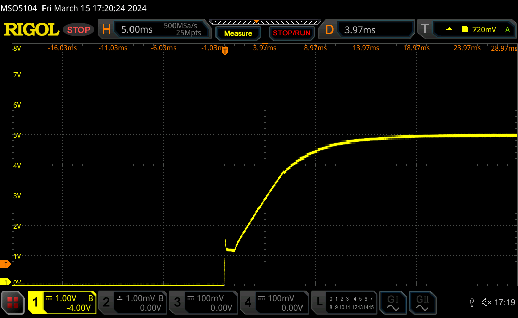
Oszilloskop-Messkurve eines Spannungsverlaufs
15 17:20:24 2024 RIGOL STOP H 5.00ms 500MSa/s 25Mpts Measure STOP/RUN D 3.97ms T 1 720mV A 8V -16.03ms -11.03ms -6.03ms -1.03ms 3.97ms 8.97ms 13.97ms 18.97ms 23.97ms 28.97ms 7V 6V 5V 4V 3V 2V 1V 1V 1.00V B 1.00mV B 100mV 100mV 0.00V 0.00V 0.00V L 0 1 2 3 4 5 6 7 8 9 10 11 12 13 14 15 GI GII 17:19
in „PPS5330 Labor-Netzteil hack“ · Mikrocontroller und Digitale Elektronik · · Oszi-Bilder

-
PDF
EW50114NCW.pdf
-15.5 , MAX = -→5 -14.5 AUG.23.2001 9 10.3 TIMING OF POWER SUPPLY AND INTERFACE SIGNAL DELETE SEP.03,2001 2 3. ABSOLUTE MAXIMUM RATINGS 3.1 ELECTRICAL ABSOLUTE MAXIMUM RATINGS VDD −VEE : MAX = 20.0→ 21.0 7 9. INTERFACE SIGNALS PIN 4 : C/→ C/D , PIN 15 : LEVEL =→HL PIN 18 : DF = “H” : LCD ON ,DF= “L”
in „Inverter für Displaybeleuchtung“ · Mikrocontroller und Digitale Elektronik ·
-
PDF
IST_TSic_20x30x_DE_V4.1.pdf
r d e Temp Temp + s u s o o 10%~90% (V = 5.0V) u ü g ( C) ( F) n r u (TSic x06) (TSic x01) (TSic x03) t b i 1 D ü h -50 -58 0x000 0.000 10% V+ (0.5V) e l n A f e -10 14 0x199 0.200 26% V+ (1.3V) . o e e s i 0 32 0x200 0.250 30% V+ (1.5V) e e i e u c 25 77 0x2FF 0.375 40% V+ (2.0V) n w s s laen 60 140
in „TSIC 206 auswerten für Anfänger“ · Mikrocontroller und Digitale Elektronik ·
-
Datei
test3.c
txt01_a_pm[] PROGMEM = "SYNC_LOSS"; const char txt02_a_pm[] PROGMEM = "OUT_OF_RANGE"; const char txt03_a_pm[] PROGMEM = "TARGET_FAILED"; const char *txtnn_a_pm[] PROGMEM = { txt00_a_pm, txt01_a_pm, txt02_a_pm, txt03_a_pm }; void getMessage(message_t* message_pt) { char c, *pt=0; //zum testen uint8_t j, l; //zum testen pt = (char*)pgm_read_word(&(txtnn_a_pm[message_pt->index])); //zum testen l = (uint8_t)strlen_P(pt); //zum testen //zum testen for ( j=0; j < l; j++ ) { c = (char)(pgm_read_byte(pt++));
in „Typvereinbahrungen, array von Zeigern auf Flash“ · Mikrocontroller und Digitale Elektronik ·
-
Datei
Programmcode.txt
} stop_i2c(); löschen mit smallprotokoll unsigned char wert=0xde; unsigned int bcc; bcc = 0x11 + 0x03 + 0x1b + 'D' + 'L' ; bcc = bcc % 256; start_i2c(); byte_out(wert); //adresse byte_out(0x11); //DC1 byte_out(0x03); //len byte_out(0x1b); //esc byte_out('D'); byte_out('L'); byte_out(bcc); //bcc stop_i2c
in „Übertragungsprobleme mit I2C und eDIP240“ · Mikrocontroller und Digitale Elektronik ·
-
PDF
Vergleich_Signal_von_SL02_mit_HP8590L18.pdf
Pegelvergleich Signal von SL02 mit HP8590L 18.12.20 Vor Versuch Warmlauf über >45 min. HP8590L wird mit interner Quelle kalibriert. Verbindungskabel ist das Original-HP-Cal-Kabel. Bei Pegeln 0 bis 13dBm zusätzlicher Abschwächer 30 dB. Bei 0 bis
in „Rohde & Schwarz SML02 Rack-Ausführung“ · HF, Funk und Felder ·
-
PDF
CA723-Intersil.pdf
C VI= 12V to 15V, - - - - - 0.3 % V O TA= 0 C to 70 C Load Regulation (Note 2) I = 1mA to 50mA - 0.03 0.15 - 0.03 0.2 % V L O I = 1mA to 50mA, - - 0.6 - - - % V L o o O TA= -55 C to 125 C L = 1mo to 50mo, - - - - - 0.6 % V O TA= 0 C to 70 C Output-Voltage Temperature Coefficient, TA= -55 C to 125 C -
in „Datenblatt suchen“ · Analoge Elektronik und Schaltungstechnik ·
-
Datei
nRF24L01_.h
now extern uint8_t lib_nRF24L01_RX_data[nRF24L01_MAX_RX_PAYLOAD_LEN]; // array for reveived data packet extern uint8_t lib_nRF24L01_RX_data_width; // number of valid (i.e. received) bytes in lib_nRF24L01_RX_data extern uint8_t lib_nRF24L01
in „nRF24L01+ Funkmodul - Auto Acknowledgement sendet keine Payload“ · Mikrocontroller und Digitale Elektronik ·
-
PDF
349_529-15.pdf
kundenseitige Welle: h6 mit 6 mm Wellendurchmesser Id.-Nr. 293328-01 Membran-Kupplung K 17 mit K 17 D1 D2 L galvanischer Trennung für Baureihe ROC/ROQ/ROD 400 Variante mit 6 bzw. 10 mm Wellendurchmesser 01 ¬ 6 F7 ¬ 6 F7 22 mm Id.-Nr. 296746-xx 02 ¬ 6 F7 ¬ 10 F7 22 mm 03 ¬ 10 F7 ¬ 10 F7 30 mm 04 ¬ 10 F7 ¬ 10
in „Wie entsteht das Sinusförmige Signal eines Drehgebers/ Vermutung“ · Offtopic ·
-
Datei
5EINSEN.LST
+1 dw val 29357+1+1 $rs 01E1 03B1 29358+1 dw val 29388+1+1 $rs 01E3 03B2 29389+1 dw val 29450+1+1 $rs 01E5 03B4 29451+1 dw val 29574+1+1 $rs 01E7 03B8 29575+1 dw val 29915+1+1 $rs 01E9 03C3 29916+1 dw val 29977+1+1 $rs 01EB 03C5 29978
in „Zähler“ · FPGA, VHDL & Co. ·
-
PDF
208_945-15.pdf
HEIDENHAIN-CERTO-Mess- Programm mit Messwegen von 25 mm taster höchste Genauigkeiten von± 0,1µm/ bei ± 0,1 µm/± 0,03 µm* Genauigkeit und ± 0,05 µm*/± 0,03 µm* für hochpräzise 60 mm bei ± 0,1 µm/± 0,05 µm* Genauig- Messungen. keit. Damit lässt sich die Anzahl der Be- Die Messtaster aus dem HEIDENHAIN- zugsnormale deutlich
in „Welchen Mikrocontroller Quadrature Decoder Kanäle ?“ · Mikrocontroller und Digitale Elektronik ·
-
PDF
208_945-15.pdf
HEIDENHAIN-CERTO-Mess- Programm mit Messwegen von 25 mm taster höchste Genauigkeiten von± 0,1µm/ bei ± 0,1 µm/± 0,03 µm* Genauigkeit und ± 0,05 µm*/± 0,03 µm* für hochpräzise 60 mm bei ± 0,1 µm/± 0,05 µm* Genauig- Messungen. keit. Damit lässt sich die Anzahl der Be- Die Messtaster aus dem HEIDENHAIN- zugsnormale deutlich
in „Wie entsteht das Sinusförmige Signal eines Drehgebers/ Vermutung“ · Offtopic ·
-
PDF
208_945-15.pdf
HEIDENHAIN-CERTO-Mess- Programm mit Messwegen von 25 mm taster höchste Genauigkeiten von± 0,1µm/ bei ± 0,1 µm/± 0,03 µm* Genauigkeit und ± 0,05 µm*/± 0,03 µm* für hochpräzise 60 mm bei ± 0,1 µm/± 0,05 µm* Genauig- Messungen. keit. Damit lässt sich die Anzahl der Be- Die Messtaster aus dem HEIDENHAIN- zugsnormale deutlich
in „SIN/COS Encoder“ · Analoge Elektronik und Schaltungstechnik ·
-
Datei
Remote_IAR.c
SetForPress(void) { P1DIR = 0xFC; // P1.0,1 inputs P1OUT = 0; // Clear P1 outputs, pull downs P1REN |= 0x03; // Enable resistors on P1.0,1 P2OUT |= 0x07; // Enable keypad P1IES &= ~0x03; // L-to-H interrupts P1IFG = 0; // Clear any pending flags P1IE |= 0x03; // Enable interrupts Error_Flags = 0; // Clear
in „MSP430 im LPM“ · Mikrocontroller und Digitale Elektronik ·