-
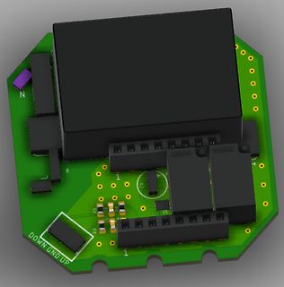
 Bild
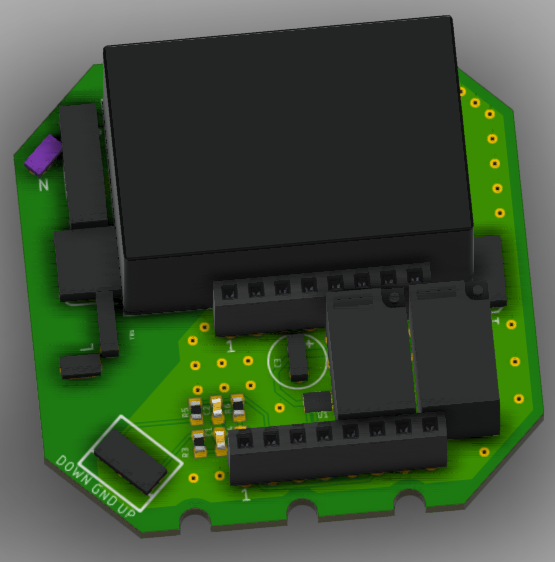
3D-CAD-Modell einer Leiterplatte mit Bauteilen
N L 1 2 3 4 5 6 7 8 9 10 11 12 13 14 15 16 17 18 19 20 21 22 23 24 25 26 27 28 29 30 31 32 33 34 35 36 37 38 39 40 41 42 43 44 45 46 47 48 49 50 51 52 53 54 55 56 57 58 59 60 61 62 63 64 65 66 67 68 69 70 71 72 73 74 75 76 77 78 79 80 81 82 83 84 85 86 87 88 89 90 91 92 93 94 95 96 97 98 99 100 101 102 103 104 105 106 107 108 109 110 111 112 113 114 115 116 117 118 119 120 121 122 123 124 125 126 127 128 129 130 131 132 133 134 135 136 137 138 139 140 141 142 143
in „Jalousie Steuerung mit Kleinspannung+ESP32“ · Mikrocontroller und Digitale Elektronik · · Layouts
-
PDF
Cube_BOTTOM.pdf
07R 41R 22R 03R 83R 7R 17R 51R 32R 13R 93R 8R 27R 61R 42R 23R 04R 9R 37R 71R 52R 33R 14R 3R 76R 11R 91R 72R 53R 51C 2R 21C 66R 9C 01R 8C 81R 01C 62R 11C 43R 05R 41C 24R 31C 15R 34R 75R 94R 65R 84R C C C C 55R 74R 45R 64R 1 1 2 2 25R 44R C C C C 35R 54R 1L 7C 1CI 13C 43C D X _ 3 1 DXT_R C TOB R
in „Cube - Bitte Schaltplan und Layout überprüfen“ · Mikrocontroller und Digitale Elektronik ·
-
Datei
ow.c
101,59,217,135,4,90,184,230,167,249,27,69,198,152,122,36,248,166,68,26,153,199,37,123,58,100,134,216,91,5,231,185, 140,210,48,110,237,179,81,15,78,16,242,172,47,113,147,205,17,79,173,243,112,46,204,146,211,141,111,49,178,236,14,80, 175,241,19,77,206,144,114,44,109,51,209,143,12,82,176,238,50,108,142,208,83,13,239,177,240,174,76,18,145,207,45,115
in „Falsche TEMP mit DS1820“ · Mikrocontroller und Digitale Elektronik ·
-
PDF
pif2_sch-1.pdf
VPP_(5v) GPIO2/I2C1_SDA TP3 4 VPP_(5v) GPIO3/I2C1_SCL 5 SCL TP4 FDONE 109 PT36D/DONE GPIO6 1 PL3A/L_GPLLT_FB FINITn 110 PT36C/INITN GPIO12 2 PL3B/L_GPLLC_FB 111 GPIO5 3 1 VDD_(3.3v) GPIO14/UART_TXD 8 GPIO14 RA9 PT35B PL4A/L_GPLLT_IN 17 10 GPIO15 LEDR 112 PT35A CE1 4 PL4B/L_GPLLC_IN VDD_(3.3V) GPIO15
in „PIF_2 MachXO2-7000HC antwortet nicht“ · FPGA, VHDL & Co. ·
-
PDF
xfft_ds260.pdf
16 16 S C N Y B - Y XC6VLX75T 803 785 1033 3 3 395 12473 31.58 1 2k R2L Y 16 16 S C N Y B - N XC6VLX75T 911 883 1084 5 2 395 26804 67.86 1 2k R2L Y 16 16 S C N Y B - Y XC6VLX75T 898 866 1086 5 3 395 26826 67.91 4 1k R2L Y 16 16 S C N Y B - N XC6VLX130T 1828 1798 2603 9 8
in „Implementierung der XILINX FFT-Core“ · FPGA, VHDL & Co. ·
-
Datei
z80.lst
, a 69: 0038 210800 ld hl, Tafel1 70: 71: 003B Loop_1inner: 72: 003B 7E ld a, (hl) 73: 003C AD xor l 74: 003D D300 out (0), a 75: 76: 77: 78: 003F 0680 ld b, 80h 79: 80: 0041 trampeln1: 81: 0041 10FE djnz $ 82: 0043 23 inc hl 83: 0044 AF xor a 84: 0045 79 ld a, c 85: 0046 17 rla 86: 0047 4F ld c, a 87: 0048 D301 out (1), a 88: 004A 30EF jr nc, Loop_1inner 89: 004C 1B dec de 90: 004D AF xor a 91: 004E BB cp e 92: 004F 20E2 jr nz, Loop_1 93: 0051 BA cp d 94: 0052 20DF jr nz, Loop_1 95: 96: 97: 0054 110002 ld de, 200h 98: 99: 0057 Loop_2: 100: 0057 0E01 ld c, 1 101: 0059 79 ld a, c 102: 005A D301
in „Hilfe bei z80 Hex Datei“ · Mikrocontroller und Digitale Elektronik ·
-
Datei
main.c
lSchranke3; volatile uint8_t bodenSensR; volatile uint8_t bodenSensL; volatile uint8_t bodenSensH; uint8_t varL1=0; uint8_t varL2=0; uint8_t varL3=0; uint8_t varL4=0; uint8_t varT1=0; uint8_t varT2=0;
in „rekursiver Funktionsaufruf verbraucht 1814 Bytes??“ · Mikrocontroller und Digitale Elektronik ·
-
Datei
main2.c
lSchranke3; volatile uint8_t bodenSensR; volatile uint8_t bodenSensL; volatile uint8_t bodenSensH; uint8_t varL1=0; uint8_t varL2=0; uint8_t varL3=0; uint8_t varL4=0; uint8_t varT1=0; uint8_t varT2=0;
in „rekursiver Funktionsaufruf verbraucht 1814 Bytes??“ · Mikrocontroller und Digitale Elektronik ·
-
PDF
TGL79XX_DATA_E.pdf
L7905C-D2TR L7905CP L7905CT (*) -5 V L7906C L7906CV L7906CD2T L7906CP (*) L7906CT (*) -6 V L7908C L7908CV L7908CD2T L7908CP (*) L7908CT (*) -8 V L7912C L7912CV L7912C-V L7912CV1 L7912CD2T L7912CP L7912CT (*) -12 V L7915C L7915CV L7915CD2T L7915CP L7915CT -15 V L7918C L7918CV L7918CD2T(*) L7918CP (*) L7918CT (*) -18 V L7920C L7920CV L7920CD2T(*) L7920CP (*) L7920CT (*) -20 V L7924C L7924CV L7924CD2T(*) L7924CP (*
in „Netzteil für Röhrenvorstufe“ · Analoge Elektronik und Schaltungstechnik ·
-
PDF
93LC56B.pdf
93LC56AX/BX are only offered in a 150-mil SOIC package. PACKAGETYPE DIP SOIC SOIC TSSOP 9 CS CS 1 L 8 1 3 8 Vcc CS 1 9 8 VCC NU 1 3 8 NC CLK 2 5 7 NCc CLK L L C DI 3 A 6 NC 2 5 7 NC CLK 2 C 7 NC Vcc 2 5 7 Vss DO 4 B 5 Vss A 6 A DI 3 / 6 NC DI 3 / 6 CS 3 B 6 B B NC X DO DO 4 5 Vss 4 5 CLK 4 5 DO Vss
in „Primo EEPROM umprogrammieren“ · Mikrocontroller und Digitale Elektronik ·
-
PDF
SPLC780D001BC.pdf
is used only for the internal oscillator operation mode. OSC 1 Rf: 75.0K±2% ( when VDD = 3.0V) Rf: 91K± 2% ( when VDD = 5.0V) OSC 2 Since the oscillation frequency varies depending1and OSCO2C pin capacitance, the wiring length to these pins should be minimized. 400 600 l H 270 z 400 t i a l y o 200
in „LCD Display initialisieren oder geht das automatisch?“ · Mikrocontroller und Digitale Elektronik ·
-
PDF
splc780D.pdf
is used only for the internal oscillator operation mode. OSC 1 Rf: 75.0K±2% ( when VDD = 3.0V) Rf: 91K± 2% ( when VDD = 5.0V) OSC 2 Since the oscillation frequency varies depending1and OSCO2C pin capacitance, the wiring length to these pins should be minimized. 400 600 l H 270 z 400 t i a l y o 200
in „2x16 LCD Batron Tabelle?“ · Mikrocontroller und Digitale Elektronik ·
-
PDF
SPLC780D.pdf
is used only for the internal oscillator operation mode. OSC 1 Rf: 75.0K±2% ( when VDD = 3.0V) Rf: 91K± 2% ( when VDD = 5.0V) OSC 2 Since the oscillation frequency varies depending1and OSCO2C pin capacitance, the wiring length to these pins should be minimized. 400 600 l H 270 z 400 t i a l y o 200
in „LCD (HD44780) timing extrem träge“ · Mikrocontroller und Digitale Elektronik ·
-
PDF
SPLC780D001BC.pdf
is used only for the internal oscillator operation mode. OSC 1 Rf: 75.0K±2% ( when VDD = 3.0V) Rf: 91K± 2% ( when VDD = 5.0V) OSC 2 Since the oscillation frequency varies depending1and OSCO2C pin capacitance, the wiring length to these pins should be minimized. 400 600 l H 270 z 400 t i a l y o 200
in „Bibliothek fuer SPLC780D“ · Mikrocontroller und Digitale Elektronik ·
-
PDF
SPLC780D.pdf
is used only for the internal oscillator operation mode. OSC 1 Rf: 75.0K±2% ( when VDD = 3.0V) Rf: 91K± 2% ( when VDD = 5.0V) OSC 2 Since the oscillation frequency varies depending1and OSCO2C pin capacitance, the wiring length to these pins should be minimized. 400 600 l H 270 z 400 t i a l y o 200
in „Datenblatt zu HD44780 1602 LCD Modul Display Anzeigen 2X16 Zeichen“ · Mikrocontroller und Digitale Elektronik ·
-
PDF
Pingu920-0.9.2.pdf
Peripheral Bus Ethernet PHY External Bus Interface +3.3V R1 10k L V 3 2 R 3 2 - - 3 2 1 4 3 2 1 0 T 1 1 1 1 C L D D D E D D D D A A A 3 3 K1 1 0 9 8 7 6 5 4 3 2 1 0 9 8 7 6 1 1 1 1 1 9 8 7 6 5 N 3 2 1 0 S S D D X O X R R X X X B B C C C S S D0 64 63 D1 D D D D D D
in „"Pingu920" - ARM9 Linux Embedded zum selbst Löten“ · Mikrocontroller und Digitale Elektronik ·
-
PDF
40146F.pdf
- Sydney Tel: 91-20-2566-1512 Tel: 33-1-69-53-63-20 Web Address: Tel: 61-2-9868-6733 Fax: 33-1-69-30-90-79 www.microchip.com Fax: 61-2-9868-6755 Fax: 91-20-2566-1513 Atlanta Japan - Yokohama Germany - Munich China -
in „Fehlersuche Funksender Zentralverriegelung Toyota Yaris“ · Fahrzeugelektronik ·
-
Datei
merlin.c
4,5 nix */ 0x00, /* 6,7 nix */ 'd', /* 8,9 D */ 'c', /* A,B C */ 'a', /* C,D A */ 'b', /* E,F B */ 'l', /* 10,11 L */ 'k', /* 12,13 K */ 'i', /* 14,15 I */ 'j', /* 16,17 J */ 'e', /* 18,19 E */ 'f', /* 1A,1B F */ 'h', /* 1C,1D H */ 'g', /* 1E,1F G */ '2', /* 20,21 2 und " */ '1', /* 22,23 1 und ! */
in „Pollin MOTOROLA VIP1710“ · Mikrocontroller und Digitale Elektronik ·
-
PDF
09600002_04_ft_55-cm-...-pnsdl-l5m_io-link_e.pdf
u u u u u u u B B t t t t t t t t S 6 5 4 3 2 1 S a o o o o o o o y D D D D D D y u g g g g g g g l l q i i i i i i i u u Q c c c c c c c Q Q i i i i i i i S wSw wSw S wS S S Signal quality level [0 ... 100 %] Q quality, threshold adjustable [0/1] Switching outputs [0/1] PROCESS DATA PROFILE 1: COLOR
in „IO-link master (light)“ · Mikrocontroller und Digitale Elektronik ·
-
PDF
91201.pdf
0.9 1.7 μC Forward Turn-On Time ton Intrinsic turn-on time is negligible (turn-on is dominatedSby L aDd L ) Notes a. Repetitive rating; pulse width limited by maximum junction temperature (see fig. 11). b. Pulse width ≤ 300 μs; duty cycle ≤ 2 %. c. Current limited by the package (die current = 130
in „Transistor für PWM 30V 50A“ · Analoge Elektronik und Schaltungstechnik ·
-
PDF
OnlinePotentiometerHandbook-1.pdf
possible and design the total effective circuit resistance varies from for that possibility. about 0.91 R2 to a little over.95Rz. 68 APPLICATION FUNDAMENTALS "ll CASEW_C AESIST"NcP"RAETERS(21 ENEAAlf 9... MINIMM(II MAlUMUM , •• , ." •• , , • ., R 't+ Rt Ar+ Rl , , •• ., CRITIC...lT ., , , _ R " + R' .,
in „Unterschied zwischen Präsizionstrimmer und Spindeltrimmer“ · Analoge Elektronik und Schaltungstechnik ·
-
 Bild
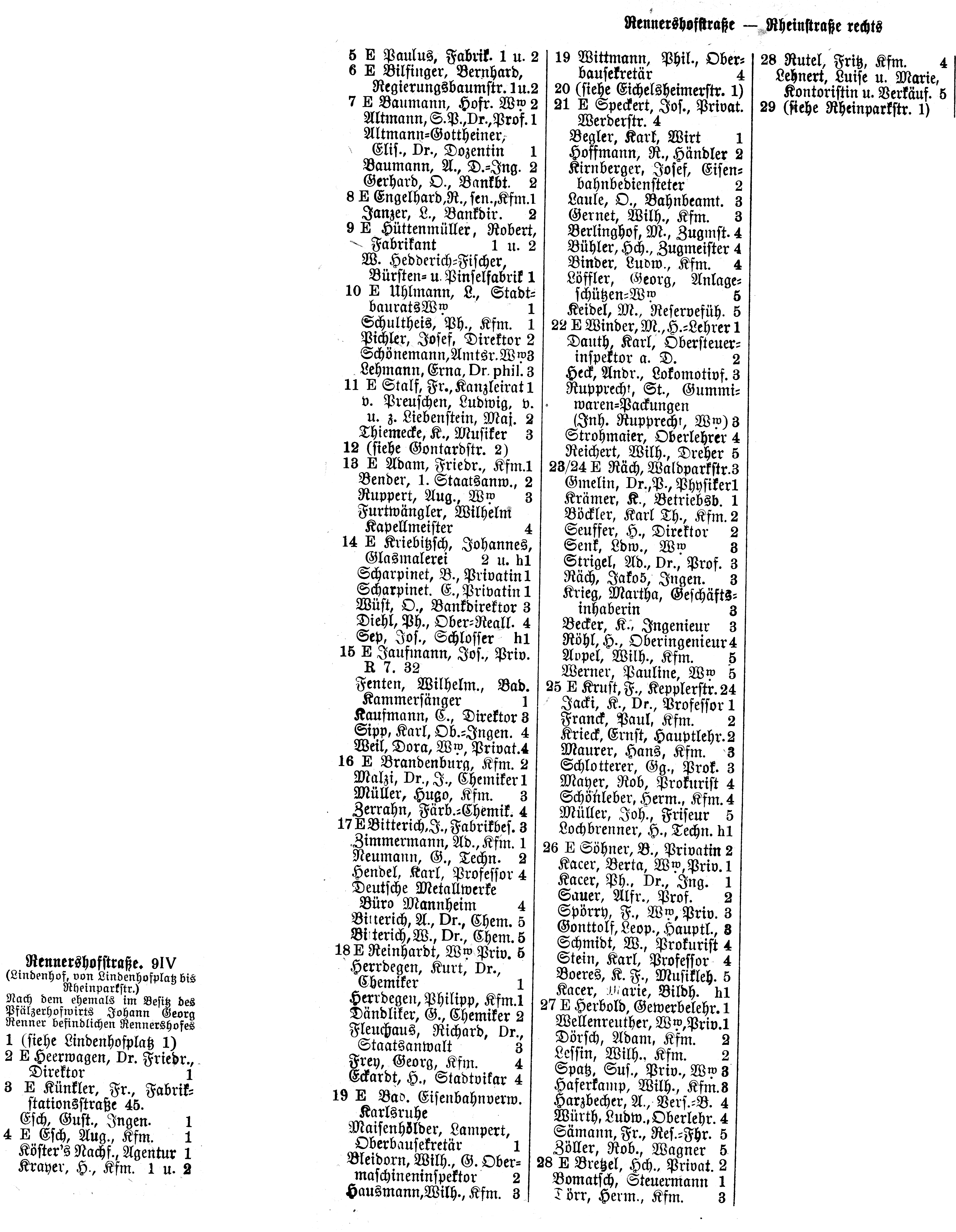
Alte Telefonbuchseite mit Namen und Adressen
Neuerdingsstraße 91V 5 E Paulus, Pabst, 1 u 2 6 E Bingert, Bernhard, Regierungsbaumeistr, 1 u 2 7 E Baumann, Hofw. 2 W Altmann, S. Dr., Prof. 1 Baumann, A., Dr., Ing. 2 Ekliff, Dr., Ingenieur 1 Engethard, R., Telekom. Janzer, L., Bankdir. 2 Eutermaier, Robert, 9 E Bürmaster, R., Ing. 2 Berlin, W., Zugst. 4 Bülker, Otto, Ingenieur 4 Binder, Ludwig, Kfm. 1 Börner, Walter, 2 W Schultis, PK., Kfm. 1 Schönemann, Anton, W. Lehmann
in „OCR für Monospace-Schrift“ · PC Hard- und Software · · Sonstiges
-
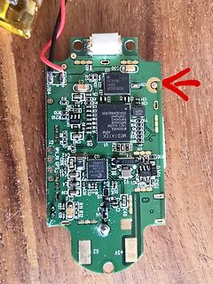
 Bild
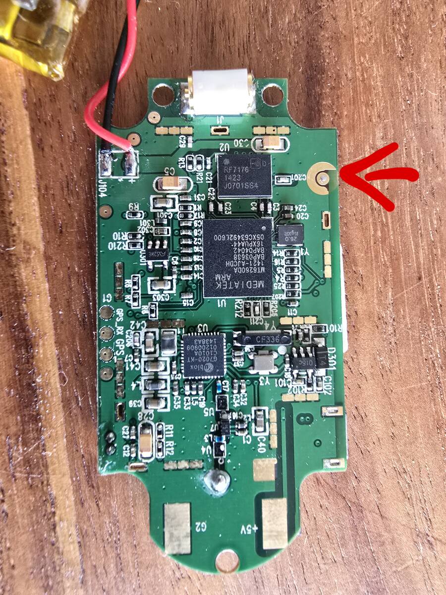
Foto einer Leiterplatte mit Mikrocontroller
U2, C30, C201, J104, R9, C301, C24, C20, R10, R210, L101, C5, C303, U1, MEDIATEK, MT6580D, 1421-A-J0H, R212, C11, R101, C102, D501, U3, C21, Y3, C40, U4, U5, R11, R12, C28, C29, C41, C42, C43, C44, C45, C46, C47, C48, C49, C50, C51, C52, C53, C54, C55,
in „TKSTAR 909 GPS Tracker - Antenne abgerissen. Neue Antenne? Aber wie?“ · HF, Funk und Felder · · Platinenfotos
-
 Bild
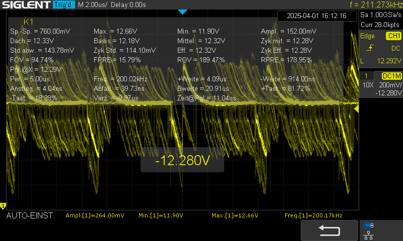
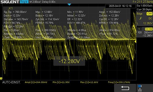
Oszilloskop Messaufnahme einer Wellenform
152.00mV CH1 Dach = 12.33V Basis = 12.18V Zyk.mit. = 12.28V Edge DC Std.abw. = 143.78mV Zyk.Eff. = 12.28V L 12.292V FOV = 94.74% FPRE = 15.79% ROV = 189.47% RPRE = 178.95% Per = 5.00us Freq = 200.02kHz +Weite = 4.09us -Weite = 914.00ns Ansteg. = 4.04ns Abfall = 39.73ns Bwite = 20.91us +Tast. = 81.72% Verz.
in „LM2596S-3.3 gibt 3.9V raus..“ · Analoge Elektronik und Schaltungstechnik · · Oszi-Bilder
-
PDF
Lattice_Timing_Closure.pdf
CLKFB2OS_D --- 0.203 *L_R26C5.CLKFB to *L_R26C5.CLKOS i_my_pll/PLLInst_0 ROUTE 1 1.632 *L_R26C5.CLKOS to *L_R26C5.CLKFB i_my_pll/CLKOS -------- 1.835 (11.1% logic, 88.9% route), 1 logic levels. PLL_R26C5.CLKOS attributes: PHASEADJ
in „IO constraints für asynchrone Inputs in Lattice Diamond“ · FPGA, VHDL & Co. ·
-
Datei
vt100.fsm.pl
print_daccept($daccept); print_code($dtrans, $daccept); } print_source_code <<'END_OF_INPUT' ESC [ ? 2 l DECANM ansiMode( false ) ESC [ ? 4 h DECSCLM softScrollingMode( true ) ESC [ ? 4 l DECSCLM softScrollingMode( false ) ESC [ Pt ; Pb r DECSTBM setMargin( (coordL) vt.parm[0], (coordL) vt.parm[1] ) ESC
in „VT100 Terminal auf dem ATmega328“ · Mikrocontroller und Digitale Elektronik ·
-
PDF
1.pdf
5 8 7 8 1 1K C83 10 R69 R70 1 22K 3 W 9 10 3 5 8 1 3 5 7 9 1 1 A _B M A W M GNDA 220p 9 10/ 5W 1K C91 10 R75 D 1 W 1 _ W 2 SV6/I D11 4 7 3 5 1 C _ S 2 2 _ S GNDA R67 220p 9 10/ 5W V W E 1 W C 1 LM3886 D12 4 7 S S E S E E 6 22K 2 4 6 8 1 1 1 R 1 LM3886 R73 1 Bass Lautstärke + MUTE R 1 22K + C85 100µ Links
in „Hilfe beim Programmieren vom Verstärker“ · Mikrocontroller und Digitale Elektronik ·
-
PDF
cc3000.pdf
Conditions Typ Max Unit VBAT = 3.6 V Tamb = +25°C 802.11b TX current Po = 18 dBm, 11 Mbps 260 275 mA L = 2048 bytes tdelay (idle) = 40 µs VBAT = 3.6 V Tamb = +25°C 802.11g TX current Po = 14 dBm, 54 Mbps 190 207 mA L = 2048 tdelay (idle) = 40 µs 802.11bg RX current VBAT = 3.6 V 92 103 mA VBAT = 3.6 V
in „Anpassnetzwerk für eine bestimmte Antenne berechnen“ · HF, Funk und Felder ·
-
Datei
AVR910.ASM
| Read data memory | 'd' | | dd | | | ;* | Chip erase | 'e' | | | 13d | | ;* | Write lock bits | 'l' | dd | | 13d | | ;* | Write fuse bits | 'f' | dd | | 13d | 11 | ;* | Read fuse and lock bits | 'F' | | dd | | 11 | ;* | Leave programming mode | 'L' | | | 13d | 5 | ;* | Select device type | 'T' | dd
in „AVRProg von Atmel und AT90S2313“ · Mikrocontroller und Digitale Elektronik ·
-
PDF
ST-L6561-Datasheet.pdf
Table 1. Order Codes ■ INTERNAL START-UP TIMER Part Number Package ■ CURRENT SENSE FILTER ON CHIP L6561 DIP-8 ■ DISABLE FUNCTION L6561D SO-8 ■ 1% PRECISION (@ T = 25°j) INTERNAL REFERENCE VOLTAGE L6561D013TR Tape & Reel ■ TRANSITION MODE OPERATION Realised in mixed BCD technology, the chip gives ■
-
Datei
blink12F629.asm
status equ 0003h fsr equ 0004h gpio equ 0005h pclath equ 000ah intcon equ 000bh pir1 equ 000ch tmr1l equ 000eh tmr1h equ 000fh t1con equ 0010h cmcon equ 0019h option_reg equ 0081h ;option equ 0081h ; backwards compatability trisio equ 0085h pie1 equ 008ch pcon equ 008eh osccal equ 0090h wpu equ 0095h
in „PIC 12F 629 ohne *inc -> wo liegt hier der Fehler verborgen?“ · Mikrocontroller und Digitale Elektronik ·
-
PDF
TSR-1_Datenblatt.pdf
1.8 VDC 82 % 69 % TSR 1-2425 4.6 – 36 VDC* 2.5 VDC 87 % 75 % TSR 1-2433 4.75 – 36 VDC* 3.3 VDC 1.0 A 91 % 78 % TSR 1-2450 6.5 – 36 VDC* 5.0 VDC 94 % 84 % TSR 1-2465 9.0 – 36 VDC* 6.5 VDC 93 % 87 % TSR 1-2490 12 – 36 VDC* 9.0 VDC 95 % 90 % TSR 1-24120 15 – 36 VDC* 12 VDC 95 % 92 % TSR 1-24150 18 – 36 VDC
in „Idee für ein ||transportables|| Handyladegerät“ · Analoge Elektronik und Schaltungstechnik ·
-
PDF
Wattuino_pro_mini_adv.pdf
1 2 3 4 VCCs I0 VCCs L1L U1U1 PIU106VCC ADC6 PIU1019 P PC6 C 6 10mH PIU104VCC ADC7 PIU1022 P PC7 C 7 A I2 OC PIU101AVCC PC0 (ADC0/PCINT8) PI24023 P PC0 C 0 A C4 20 PC1 (ADC1/PCINT9) PI25024 P PC1 C 1 I2 COC GND PIC401 PIC402
in „RFM12 Empfang (nicht schon wieder.)“ · Mikrocontroller und Digitale Elektronik ·
-
PDF
JSPHS-661_.pdf
5.0 159.07 136.75 67.58 1.51 1.09 1.35 1.09 1.27 1.56 Tolerance to be within ±.002 6.0 178.10 170.91 105.08 1.55 1.08 1.15 1.07 1.13 1.51 7.0 189.31 192.06 141.95 1.57 1.10 1.03 1.04 1.06 1.40 8.0 196.02 204.60 169.46 1.59 1.13 1.09 1.06 1.02 1.28 9.0 200.35 212.48 188.21 1.60 1.15 1.11 1.07 1.00 1.18
-
PDF
SMD_Sortiment02-Zusammenstellung.pdf
213AB) 100 ab Lager SM4004SMD 90 Schaltdiode, Si 100V/0,15A Minimelf SOD-80 200 ab Lager LL4148SMD 91 Z-Diode 500mW/3,6V Minimelf SOD-80 40 ab Lager BZV55/3,6V 92 Z-Diode 500mW/5,6V Minimelf SOD-80 40 ab Lager BZV55/5,6V Transistoren SMD 93 NPN 45V 0,5A 0,25W B:250-600 SOT23 120 ab Lager BC817/40SMD 94 PNP 45V 0,5A 0,25W B:250-600 SOT23 40 ab Lager BC807/40SMD 95 N-Kanal MOSFET N-LogL 20V 4,2A SOT23 20 ab Lager IRLML2502SMD 96 P-Kanal MOSFET P-LogL 20V 3,7A SOT23 20 ab Lager IRLML6402SMD
in „SMD Sammelbestellung, SMD Starterpack, SMD Grundausstattung, SMD Bauteile, Baugröße 0805 (zweite)“ · Markt ·
-
PDF
2450.pdf
1.8 VDC 82 % 69 % TSR 1-2425 4.6 – 36 VDC* 2.5 VDC 87 % 75 % TSR 1-2433 4.75 – 36 VDC* 3.3 VDC 1.0 A 91 % 78 % TSR 1-2450 6.5 – 36 VDC* 5.0 VDC 94 % 84 % TSR 1-2465 9.0 – 36 VDC* 6.5 VDC 93 % 87 % TSR 1-2490 12 – 36 VDC* 9.0 VDC 95 % 90 % TSR 1-24120 15 – 36 VDC* 12 VDC 95 % 92 % Models TSR 1-24150 18
in „Power Supply für Raspberry Pi 3b“ · Mikrocontroller und Digitale Elektronik ·
-
PDF
STA508.pdf
pin to Vdd pin, as single bridge with double current load.Theinputpinshavethresholdproportional toV L capability, and as half bridge (Binary mode) with half pin voltage. current capability. Figure 2. Block Diagram +V VCC1A CC 15 C30 C55 IN1A IN1A 29 M3 1µF 1000µF 17 L18 22µH +3.3V VL 23 OUT1A CONFIG
in „Heimkino ( Harman Hs 250 defekt )“ · Analoge Elektronik und Schaltungstechnik ·
-
PDF
IS2200E_V1.61.pdf
Power Supply Control Register 6 ʢR29ʣ %▯▯ %▯▯ %▯▯ %▯▯ %▯▯ %▯▯ %▯▯ %▯▯ ▯ ▯ ▯ ▯ ▯ 4$/▯▯ 4$/▯▯ 4$/▯▯ R/L, SCN2 ʕ SCN0: Specify the gate scan mode. R/L SCN2 SCN1 SCN0 Scan Mode 1 1 1 1 MODE1R 0 1 1 1 MODE1L 1 0 1 1 MODE2R 0 0 1 1 MODE2L 1 1 0 1 MODE3R 0 1 0 1 MODE3L 1 0 0 1 MODE4R 0 0 0 1 MODE4L 1 1 X 0
in „LCD-Modul OPTREX 351570AG“ · Mikrocontroller und Digitale Elektronik ·
-
PDF
70622B.pdf
O O L L S z µ 1 E E C C C L L E H C 4 3 T T V V V P P T X M . 1 2 3 4 5 6 7 8 2 0 1 4 1 1 b 1 1 T R Ω L 1 e S n n L . . l 6 5 4 e a 3 Ω % l L S T 1 F R k 1 4 a C µ 6 H H C T . n L 8 6 e 0 o 6 5 S d e p H 5 e L e e L 2 0 C e b S b C F d 1 1 S T T 0 L 6 n F F a 4 p p , C 2 3 6 5 4 C F 1 D T D µ C e G O G 0 , b 1 5 p p L T C C . . F r 2 1 e N N f . S G IN G s c 1 2 3 e n 1 1 8 l a F 3 3 v e B B t p n i z z 1
in „Wie genau funktioniert die drahtlose Kommunikation?“ · HF, Funk und Felder ·
-
 Bild
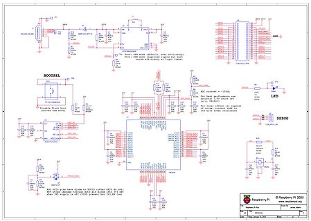
Schaltplan einer Elektronikschaltung mit Raspberry Pi Pico
R66 R67 R68 R69 R70 R71 R72 R73 R74 R75 R76 R77 R78 R79 R80 R81 R82 R83 R84 R85 R86 R87 R88 R89 R90 R91 R92 R93 R94 R95 R96 R97 R98 R99 R100 L1 D1 U1 LED1 J0
in „I/O-Beschaltung Raspberry Pico (für 24V)“ · Mikrocontroller und Digitale Elektronik · · Schaltpläne
-
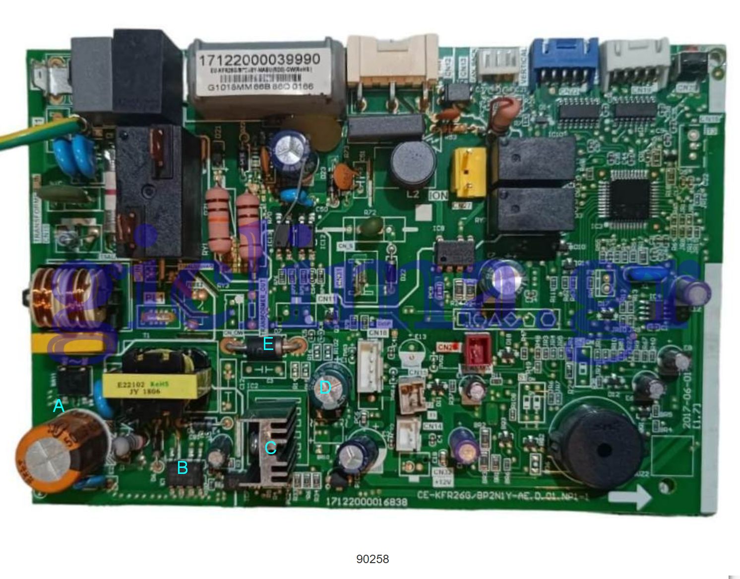
 Bild
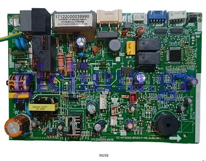
Foto einer bestückten Leiterplatte mit Bauteilmarkierungen
17122000039990 G1018MM6B B60 0166 E23102 K4HS JV 1866 L2 ION CN1 CN2 CN3 CN10 CN16 CN17 CN18 CN19 CN20 CN21 CN22 CN23 CN24 CN25 CN26 CN27 CN28 CN29 CN30 CN31 CN32 CN33 CN34 CN35 CN36 CN37 CN38 CN39 CN40 CN41 CN42 CN43 CN44 CN45 CN46 CN47 CN48 CN49 CN50 CN51
in „Reparatur Split-Klima - SNT - Diode SR315“ · Analoge Elektronik und Schaltungstechnik · · Platinenfotos
-
 Bild
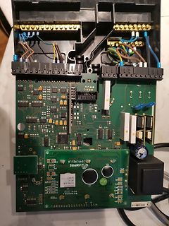
Leiterplatte eines elektronischen Steuergeräts mit Verdrahtung
AMPIRE 16A1REU,A 08.47 L710K(R) AC684111 U2 U3 U10 U11 U12 U13 U14 U15 U16 U17 U18 U19 U20 U21 U22 U23 U24 U25 U26 U27 U28 U29 U30 U31 U32 U33 U34 U35 U36 U37 U38 U39 U40 U41 U42 U43 U44 U45 U46 U47 U48 U49 U50 U51 U52 U53 U54
in „PAW Frischwassermodul“ · Haus & Smart Home · · Platinenfotos
-
PDF
OLED_12832.pdf
1 2 3 4 A A Active Area 0.91" 128*32 pixels H U1 T E M P N P N A R S D S K A E O C SSD1306 C C C C V V V V R S S I V V B 1 2 3 4 5 6 7 8 9 1 1 1 1 1 B C2 C1 R1 V E C D C4 1uF 1uF C GND S L K 560K2.2uF VCC VCC GNDGND J1 U2 VCC VCC
in „[Bascom] ATMega328 und Software I2C steuern“ · Mikrocontroller und Digitale Elektronik ·
-
PDF
LM334.pdf
L M March 2000 1 3 / M LM134/LM234/LM334 3 4 3-Terminal Adjustable Current Sources L M General Description LM234-6 are specified as true temperature sensors with The LM134/LM234/LM334 are 3-terminal adjustable
-
PDF
RDA5807SP.pdf
at3.3Vpowersupply l Autonomoussearchtuningfunction l Supportworldwidefrequencyband l Bassboost Ø 76-108MHz l Standbymode l Digitallow-IFtuner l Programmablede-emphasis(50/75μs) Ø Image-rejectdown-converter l Directlysupport32Ωresistanceloading
in „Hilfe benötigt bei RDA5807SP Ansteuerung“ · Mikrocontroller und Digitale Elektronik ·
-
Datei
terminal.txt
" missing on display ":1.0". fixme:actctx:parse_depend_manifests Could not find dependent assembly L"Microsoft.VC80.MFCLOC" fixme:actctx:parse_depend_manifests Could not find dependent assembly L"Microsoft.VC80.MFCLOC" fixme:actctx:parse_depend_manifests Could not find dependent assembly L"Microsoft.VC80
-
PDF
5821.pdf
Output Input I1 I2 I3 ..........8...Enable I1 2 I3 ..........I8.. H H R R .............. R R 1 2 7 7 L L R 1 R2 ...........7.. R R 7 X R 1 R 2 R3 ...........8.. R R 8 X X X .............. X X L R 1 R 2 R 3 ..........8... R P P P .............. P P H P P P .............. P L P P P .............. P 1 2 3 8 8 1 2 3 8 1 2 3 8 X X X .............. X H H H H .............. H L = Low Logic Level H = High Logic Level X = Irrelevant P = Present State R = Previous State 115 Northeast Cutoff, Box 15036 Worcester, Massachusetts 01615-0036 (508) 853-5000 5821 AND 5822 8-BIT SERIAL-INPUT
in „Datenblatt vom UCN5821A gesucht“ · Mikrocontroller und Digitale Elektronik ·
-
Datei
testfatread.c
PartStart = sector; sector += SwapReadWord(BootSect,wReservedSectors); sector += (SwapReadLong(BootSect,lSectorsPerFat) * BootSect[bNumberOfFats]); PartDataStart = sector; Rootcluster = SwapReadLong(BootSect,lRootCluster); MaxCluster = BootSect[bSectorsPerCLuster]; return 0; } return ERR_FAT_ERROR; //not
in „uC für 0,20€ CH552 / CH554 von WCH Billig Micro mit USB Funktion, Chip vorstellung“ · Mikrocontroller und Digitale Elektronik ·
-
PDF
EP4CE22_pin-out.pdf
VREFB1N0 IO DIFFIO_L4n D1 B1 VREFB1N0 nSTATUS nSTATUS F4 9 B1 VREFB1N0 IO G5 B1 VREFB1N0 IO DIFFIO_L5p F2 B1 VREFB1N0 IO DIFFIO_L5n F1 B1 VREFB1N0 IO DIFFIO_L6p G2 10 DQS0L/CQ1L,DPCLK0 DQS0L/CQ1L,DPCLK0 DQS0L/CQ1L,DPCLK0